HAL Id: hal-02086422
https://hal.archives-ouvertes.fr/hal-02086422
Submitted on 3 Apr 2019
HAL is a multi-disciplinary open access
archive for the deposit and dissemination of
sci-entific research documents, whether they are
pub-lished or not. The documents may come from
teaching and research institutions in France or
abroad, or from public or private research centers.
L’archive ouverte pluridisciplinaire HAL, est
destinée au dépôt et à la diffusion de documents
scientifiques de niveau recherche, publiés ou non,
émanant des établissements d’enseignement et de
recherche français ou étrangers, des laboratoires
publics ou privés.
Ygor Quadros de Aguiar, Frédéric Wrobel, Jean-Luc Autran, Paul Leroux,
Frédéric Saigné, Antoine Touboul, Vincent Pouget
To cite this version:
Ygor Quadros de Aguiar, Frédéric Wrobel, Jean-Luc Autran, Paul Leroux, Frédéric Saigné, et al..
Impact of Complex-Logic Cell Layout on the Single-Event Transient Sensitivity. IEEE RADECS2018,
Sep 2018, Goteborg, Sweden. �hal-02086422�
Abstract—The design methodology based on standard cells is
widely used in a broad range of VLSI applications. Further, several optimization algorithms can be employed to address different constraints such as power consumption or reliability. This work evaluates the implications of the usage of complex-logic cells from a 45 nm Standard-Cell library to the Single-Event Transient sensitivity under heavy ions. Results show that even though a reduction in the layout area is obtained when adopting complex-logic gates, a slight reduction in the total sensitive area of the circuit is observed. Moreover, the effectiveness of logical masking can be suppressed, leading to a higher SET cross-section.
Index Terms— Complex-logic gate, Heavy ions, Logical
Masking, Monte-Carlo simulation, Single-Event Transient
I. INTRODUCTION
HE constant scaling process of transistors has provided great achievements in terms of computational power. The design abstraction provided in a cell-based methodology for the design of Application-Specific Integrated Circuits (ASICs) enabled the development of highly integrated and complex devices, so-called Very-Large-Scale Integration (VLSI) systems. In this methodology, a Standard-Cell library containing thousands of pre-designed and characterized logic gates is used in the logic synthesis of the circuit design [1]. However, as devices are reaching the nanometer scale, reliability issues are exacerbated such as increased soft error rates and pronounced Short-Channel Effects (SCEs) [2, 3]. For instance, dedicated effort towards the reduction of the increased static power dissipation due to excessive leakage currents induced by SCEs is vastly investigated [4, 5]. Additionally, the effectiveness of soft error mitigation techniques is reduced due to multi-node charge collection and multiple bit upsets [6-9]. Apart from the dedicated leakage current mitigation schemes, the reduction of the number of transistors can be an effective way to improve the reliability and power consumption of VLSI designs at advanced
Manuscript received April 20, 2018. This work has received funding from the European Union’s Horizon 2020 research and innovation programme under the Marie-Skolodowska-Curie grant agreement number 721624.
Y. Q. Aguiar, F. Wrobel, F. Saigné, A. D. Touboul and V. Pouget are with IES, Université de Montpellier, CNRS, Montpellier, France (corresponding author e-mail: [email protected]).
J-L. Autran is with the Institut Materiaux Microelectronique Nanoscience de Provence, Aix-Marseille University, Marseille, France.
P. Leroux is with the Advanced Integrated Sensing Lab, KU Leuven University, Leuven, Belgium.
technology nodes. By reducing the transistor count for a given circuit, the number of connections is also reduced leading to relaxed cell routing and improved reliability regarding physical manufacture failures [10]. Although the advantages of reducing the transistor count in a VLSI design is well-known, the impact to radiation sensitivity has not been widely analyzed yet. Denser layouts and the reduced number of transistors can be achieved by using complex-logic CMOS gates [10, 11]. Most of the works in the literature have focused only on the study of radiation effects in basic logic cells such as NAND, NOR and INV gates. Given the significance of charge sharing due to the multi-node collection at deeply scaled technologies, it is imperative to study the Single-Event Transient (SET) sensitivity of complex-logic gates at digital circuits. Therefore, this work aims to evaluate the impact of using complex gates from a Standard Cell library to the radiation reliability of VLSI designs.
II. COMPLEX-LOGIC CMOSGATES
Different from the full custom layout design approach, standard-cell based methodology can improve the design implementation time with a fair reduction in performance and area [1]. However, during the logic synthesis, a given Boolean function can be implemented in many different combinations of logic cells, resulting in a different number of transistors and layout designs which directly impact the radiation robustness of the circuit. Accordingly, a standard-cell library contains multiple implementations of the same logic function, differing in area, performance and reliability [10]. The variety provided by the cell library can be used to accomplish different optimization constraints, for instance, targeting radiation robustness.
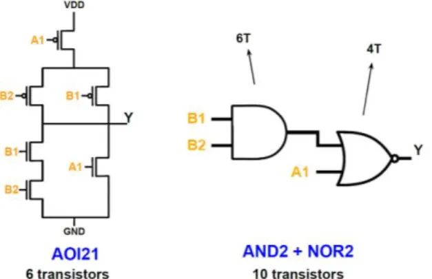
The usage of complex logic gates commonly available at cell libraries, such as the And-Or-Inverter (AOI) and Or-And-Inverter (OAI) cells, reduces the number of transistors and provides denser layouts reducing power consumption and area [10]. For example, the Boolean logic function given in Eq. 1 can be implemented by using basic logic standard cells as NAND, NOR and INV or by using the complex-gate AOI directly.
𝑌 = ¬(𝐴1 ˄ (𝐵1 ˅ 𝐵2)) (1) As shown in Fig. 1, the AOI21 implementation of Eq.1 contains 40% of reduction in the transistor count compared with the implementation using an AND2 gate coupled with a NOR2 gate. Clearly, the power consumption for the AOI21
Impact of Complex-Logic Cell Layout on the
Single-Event Transient Sensitivity
Y. Q. Aguiar, F. Wrobel, J-L. Autran, P. Leroux, F. Saigné, A. D. Touboul and V. Pouget
gate is also reduced, but the sensitivity to radiation is not straightforward to be predicted in advance. In [11], an optimizing synthesis methodology is proposed to reduce the transistor count of circuits. The proposed methodology is called Gate Clustering and consists in the agglutination of basic logic gates into static CMOS complex gates (SCCG) [11]. The authors confirm that the reduced number of transistor improves the power consumption and layout area. Further, the circuit performance is also improved due to the reduction of the circuit wirelength which is the main source of delay at advanced technology nodes [12, 13]. Due to complex SET dependencies, as the node capacitance, charge sharing, pulse quenching and particle energy, the radiation sensitivity of these implementations must be analyzed at layout level. For instance, the charge sharing induced by the multi-node charge collection in deeply scaled CMOS transistors can improve the radiation robustness by reducing the SET cross-section and the transient pulse width due to the Pulse Quenching Effect [14]. However, it can also worsen the design reliability by inducing multiple SET (MSET) and limiting the effectiveness of hardware techniques based on redundancy or even invalidating hardening schemes such as conventional Error Correcting Codes (ECCs) for memory elements [8].
In the literature, most of the studies generally concentrate to analyze basic CMOS logic combinatorial functions such as NAND, NOR or INV. A comparative analysis of NAND and NOR gates in bulk FinFET devices can be found in [15]. Different drive strength and supply voltages were used to investigate the SET sensitivity of these circuits. As expected, the increase of the drive strength or the supply voltage can shorten the SET pulse width, but with a penalty in the power consumption [15]. In [16], experimental results for NAND, NOR and INV logic gates in 90nm are provided for protons and heavy ion irradiation. Also, distinct SET robustness was observed for each gate due to the different drain sensitive areas and topology of the circuits [16]. However, the SET characterization in cell-based designs requires not only the analysis of these basic logic structures. Thus, a complex-logic CMOS gate is analyzed and compared with the usage of basic logic cells.
III. METHODOLOGY
This work aims to investigate the SET sensitivity of denser layouts provided by complex-logic cells in a Standard-Cell library. For this reason, the circuit implementations of Fig. 1
simulation chain is divided into two steps: first, the particle interaction simulation; second, the electrical simulation to account for the circuit response effects. For the first step, the MC-Oracle, a predictive tool based on Monte-Carlo simulations, is adopted to calculate the transient currents generated from the particle interaction within the devices [18, 19]. Besides the radiation environment specification, the tool requires the layout information contained in the GDS (Graphical Design System) format file, so the geometric structures of the sensitive volumes can be extracted directly from the design. In the second step, the SET database generated by MC-Oracle is injected by SPICE simulations considering the post-layout parasitic extraction netlist of the two design implementations of Fig. 1. Thus, the proposed simulation chain is able to consider the response from the particle interaction physics to the electrical circuit effect in order to accurately predict the radiation sensitivity of digital circuits. The cell drive strength of all analyzed logic gates was chosen to be the minimum strength available in the library cell. For all the electrical simulations, an inverter was coupled to the output signal in which the SET pulse was measured, i.e. all circuits were driving a fan-out 1 (FO1). The calculation of the SET cross-section used in this work only considers the transient pulses that have reached half the value of the nominal supply voltage. The heavy ions simulated by MC-Oracle were chosen for a range from 0.84 to 78.23 MeV.cm2/mg.
IV. RESULTS AND DISCUSSION
To understand the individual behavior of the p-type and n-type devices in this study, the simulations were divided into two groups: the P-hit simulations, for which all the PMOS devices are turned off, i.e. input vector set to (1, 1, 1); and the N-hit simulations, for which all the NMOS devices are turned off, i.e. input vector set to (0, 0, 0). For instance, in the P-hit simulations, exclusively all the P-type transistors are sensitive to SET, i.e. all observed transient pulse is generated from a particle hit over the drain region of a PMOS transistor. The information of the P-hit and N-hit sensitive area can be found in Table 1 along with the value of the layout area and total sensitive area of each logic gate. The sensitive area refers to the area of the drain p-n junctions extracted from the layout circuit design and imported to the MC-Oracle tool. Notice that the complex-gate AOI21 provides a reduction of
Table 1
Total area for each cell layout design, total sensitive region and P-hit and N-hit sensitive area (µm2)
Layout Area Total Sensitive Area P-hit Sensitive Area N-hit Sensitive Area NOR2 0.879 0.212 0.154 0.058 AND2 1.196 0.205 0.110 0.095 AOI21 1.196 0.359 0.242 0.116 AND + NOR 2.075 0.418 0.264 0.153
Fig. 1. CMOS transistor structure of the complex-logic AOI21 gate and its correspondent implementation with an AND2 gate and NOR2 gate.
approximately 42% in the total layout area, as it was expected. However, it provides solely 14% reduction of the total sensitive area in which is responsible for the charge collection during a particle interaction into the silicon. The AND+NOR implementation has the largest sensitive area while the AND gate presents the smallest sensitive area.
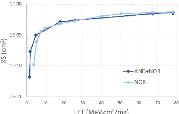
The SET cross-section considering only P-hit interactions is shown in Fig. 2. It clearly shows that the implementation containing the basic logic cells AND+NOR provides a lower SET cross-section than the AOI21 for the entire LET range. Both circuits present the same threshold LET whereas there is a SET cross-section difference of approximately a factor of 2. The charge sharing effect and more importantly the logical masking [20] between the AND gate and NOR gate are responsible for this reduced number of observed SET in the output of the AND+NOR implementation. Any SET induced at the AND gate will be filtered by the logic of the NOR gate as observed in the truth table shown in Fig. 3. The output of the NOR gate will remain at logic zero as long as the secondary input remains at logic one. As it will be shown further in the results, this masking effect is not observed for the N-hit configuration.
By analyzing the P-hit sensitive area of the two implementations presented in Table 1, both the AND+NOR and AOI21 gate present approximately the same sensitive area, a difference of only 2%. However, by analyzing the structure of the combinational logic and the electrical
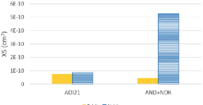
simulation results, the SETs observed for the AND gate are logically masked by the NOR gate, thus reducing the overall drain sensitive area to the PMOS devices issued in the NOR gate. The Fig. 4 presents the comparison between the SET cross-section of the AND+NOR implementation and the standalone NOR gate. It can be observed that the logical masking is effective by reducing the sensitivity of the circuit close to the sensitivity of the standalone NOR gate. However, the AND+NOR implementation presented a lower threshold LET than the NOR gate due to the charge sharing between the AND gate and the NOR.
Considering only the N-hit interactions, the SET cross-sections are approximately the same for high LET ions as illustrated in the Fig. 5. Table 1 indicates that both circuits present very similar N-hit sensitive area. Further, in this case study, there is no contribution of logical masking effect. The NOR gate output is determined whenever one of its input is at logic one. Then, as originally both inputs are set to logic zero, whenever a generated SET at the AND gate propagates to the NOR gate, it will be able to propagate to its output in case of not being electrically attenuated.
For ion LET lower than 5 MeV.cm2/mg, the difference in
the sensitive area between the analyzed circuits becomes more evident. For instance, the complex-logic AOI21 gate has approximately 24% of reduced N-hit sensitive area and it reaches about 57.3% and 83.7% reduction on the SET
cross-Fig. 2. SET cross-section of P-hit interactions for the complex-logic AOI21 gate and AND+NOR implementation.
Fig. 5. SET cross-section of N-hit interactions for the complex-logic AOI21 agate and AND+NOR implementation.
Fig. 3. Logical Masking Effect for the P-hit configuration in the combinational logic circuit AND+NOR. There is no logical masking when both inputs are set to logic zero.
Fig. 4. Comparison of SET Cross-section of the AND+NOR implementation and the standalone NOR gate.
section for LET= 2.52 MeV.cm2/mg and LET = 1.69
MeV.cm2/mg, respectively. Fig. 6 displays a comparison of
the SET cross-section of both circuits for P-hit and N-hit interaction under heavy ion of LET = 78.23 MeV.cm2/mg. The
results show that the complex-logic AOI21 gate presents a slight difference regarding the strike device which can be attributed to its symmetric topology of the up and pull-down transistor networks. Unlikely, the AND+NOR implementation presents a difference of approximately 43% between the P-hit and N-hit SET cross-section.
The comparisons with LET = 1.69 MeV.cm2/mg is depicted
in Fig. 7. For lower LET, the AOI21 gate shows an even smaller difference between the two hit interactions. In contrary to the higher LET result, now the N-hit SET cross-section is greater than the P-hit one. Moreover, the low LET ion induced a pronounced difference between the results for the AND+NOR implementation. About 91.7% greater than the P-hit SET cross-section, the circuit shows a higher sensitivity to the N-hit configuration despite the reduced N-hit drain sensitive area as shown in Table 1.
V. CONCLUSIONS
The cell-based design methodology is widely used for a wide range of VLSI applications. Due to the plurality of pre-designed and characterized standard cells, different optimization algorithms can be implemented to address several constraints such as power consumption, performance and reliability. Different from the most studies in the literature, this work proposed to analyze the implications of
provides a denser design with reduction in the power consumption and area. Further, the complex-gate AOI21 gate showed a quite similar sensitivity for the P-hit and N-hit interactions, in contrast with its counterpart implementation. However, the reduction of the layout design area does not reduce significantly the overall drain sensitive area of the circuit, leading to a similar or worse robustness than an implementation using basic logic cells. Additionally, the complex-logic gate limits the effectiveness of logical masking inherent in combinational logic circuits.
REFERENCES
[1] B. Kick et al., “Standard-Cell-based design methodology for high-performance support chips,” in IBM J. Res. Develop., vol. 41, 1997. [2] P. E. Dodd et al., “Current and future challenges in radiation effects on
CMOS electronics,” in IEEE TNS, vol. 57, pp 1747-1763, 2010. [3] G. Hubert, L. Artola and D. Regis, “Impact of Scaling on the soft error
sensitivity of bulk, FDSOI and FinFET technologies due to atmospheric radiation,” in Integration, the VLSI Journal, vol. 50, pp 39-47, Jan. 2015. [4] H. F. Dadgour, S. C. Lin and K. Banerjee, “A statistical framework for estimation of full-chip leakage-power distribution under parameter variations,” IEEE Transactions on Electron Devices, vol. 54, no. 11, pp. 2930-2945, Nov. 2007.
[5] K. Roy et al., “Leakage current mechanisms and leakage reduction techniques in deep-submicrometer CMOS circuits,”
[6] O. A. Amusan et al., “Charge collection and charge sharing in a 130nm CMOS technology,” in IEEE TNS, vol. 53, pp 3253-3258, 2006. [7] J. D. Black et al., “Characterizing SRAM single event upset in terms of
single and multiple node charge collection,” in IEEE TNS, vol. 55, pp 2943-2947, Dec. 2008.
[8] S. Pagliarini, F. Kastensmidt, et al., “Analyzing the impact of single-event-induced charge sharing in complex circuits,” in IEEE TNS, vol. 58, pp 2768-2775, 2011.
[9] J. D. Black, P. E. Dodd and K. M. Warren, “Physics of Multiple-Node Charge Collection and Impacts on Single-Event Characterization and Soft Error Rate Prediction,” in IEEE TNS, vol. 60, pp 1836-1851, May 2013.
[10] R. Reis, “Power Consumption and Reliability in NanoCMOS,” in IEEE International Conference on Nanotechnology, 2011, pp. 711-714. [11] C. Conceição, G. Posser and R. Reis, “Reducing the Number of
Transistors with Gate Clustering,” in IEEE LASCAS, Florianopolis, 2016, pp. 163-166.
[12] G. Flach, M. Fogaça, J. Monteiro et al., “Drive Strength Aware Cell Movement Techniques for Timing Driven Placemente,” in International Symposium on Physical Design (ISPD), 2016, pp. 73-80.
[13] M. Fogaça et al., “Quadratic timing objectives for incremental timing-driven placement optimization,” in IEEE ICECS, 2016, pp. 620 – 623. [14] J. R. Ahlbin et al., “Single-Event transient pulse quenching in advanced
CMOS logic circuits,” in IEEE TNS, vol. 56, pp 3050-3056, 2009. [15] L. Artola, G. Hubert, and M. Alioto, “Comparative soft error evaluation
of layout cells in FinFET technology,” Microelectronics Reliability, v. 54, pp 2300 – 2305, 2014.
[16] E. H. Cannon and M. Cabanas-Holmen, "Heavy Ion and High Energy Proton-Induced Single Event Transients in 90 nm Inverter, NAND and NOR Gates," in IEEE TNS, vol. 56, no. 6, pp. 3511-3518, Dec. 2009.
[17] J. Stine et al., “FreePDK: an open-source variation-aware design kit,” in IEEE MSE, pp. 173-174, 2007.
[18] F. Wrobel and F. Saigné, “MC-Oracle: a tool for predicting Soft Error Rate,” in Computer Physics Communications, v. 182, pp. 317 – 321, Elsevier, 2011.
[19] F. Wrobel et al., "Determining Realistic Parameters for the Double Exponential Law that Models Transient Current Pulses," in IEEE TNS, vol. 61, no. 4, pp. 1813-1818, Aug. 2014.
[20] Quming Zhou and K. Mohanram, "Cost-effective radiation hardening technique for combinational logic," in IEEE/ACM International Conference on Computer Aided Design (ICCAD), 2004, pp. 100-106. Fig. 6. Comparison of the SET cross-section of the complex-logic AOI21
gate and AND+NOR implementation considering P-hit and N-hit simulations under LET = 78.23MeV.cm2/mg.
Fig. 7. Comparison of the SET cross-section of the complex-logic AOI21 gate and AND+NOR implementation considering P-hit and N-hit simulations under LET = 1.69MeV.cm2/mg.