HAL Id: hal-00193467
https://hal.archives-ouvertes.fr/hal-00193467
Submitted on 3 Dec 2007
HAL is a multi-disciplinary open access
archive for the deposit and dissemination of
sci-entific research documents, whether they are
pub-lished or not. The documents may come from
teaching and research institutions in France or
abroad, or from public or private research centers.
L’archive ouverte pluridisciplinaire HAL, est
destinée au dépôt et à la diffusion de documents
scientifiques de niveau recherche, publiés ou non,
émanant des établissements d’enseignement et de
recherche français ou étrangers, des laboratoires
publics ou privés.
60GHz Interdigitated SOI integrated dipole antenna
with a CPW balun
Moussa Barakat, Christophe Delaveaud, Fabien Ndagijimana
To cite this version:
Moussa Barakat, Christophe Delaveaud, Fabien Ndagijimana. 60GHz Interdigitated SOI integrated
dipole antenna with a CPW balun. Mediterranean Microwave Symposium 2006, Sep 2006, Genova,
Italy. �hal-00193467�
60GHz Interdigitated SOI integrated dipole
antenna with a CPW balun
Moussa Barakat
1, 2, Christophe Delaveaud
1, Fabien Ndagijimana
2 Laboratory of Electronics and Information Technology (LETI1), French Atomic Energy Commission (CEA), 38054 Grenoble Cedex 9, France[email protected];[email protected]. Telephone: +33438785647; Fax: +33438785159
Institute of Microelectronics, Electromagnetism and Photonics (IMEP2) Minatec - INPG ,3 Parvis Louis Néel ,BP 257 F - 38016 Grenoble Cedex 1
Abstract
In this paper, we propose a 60 GHz fully integrated dipole antenna on 0.13 µm silicon on insulator (SOI) substrate, incorporating an interdigitated capacitor. An integrated balun has been designed on the top level layer to assure a compatibility with the test devices. The balun is completely characterized on SOI substrate for subsequent de-embedding of the antenna impedance. The design was based on electromagnetic simulations made using the CST Microwave Studio software package. The antenna exhibits an excellent impedance matching to 50 Ohms at 60GHz with a bandwidth of 10%. The radiation of the integrated structure has been carefully studied and optimisation of the efficiency has been obtained using the back side metallization under the wafer as a reflector. The resulting radiation efficiency is 90 % with a gain around 4.45 dBi .
Index Term—Dipole antenna, Silicon on insulator, coplanar waveguide, balun, millimetre wave antennas
I. INTRODUCTION
Over the last decades, technological advances have promoted exponential decrease in the size of computational functionality, rapid growth in the number of networked devices, diminishing wireless devices sizes and a continual decline in cost. The utilization of millimetre wave frequencies enables the design of compact, lightweight, and low cost wireless millimetre wave communication front-ends which can offer convenient terminal mobility and high capacity channel. A 60-GHz band is attractive candidate for short range radar and indoor communications based on pico cell zone because it has high atmospheric loss.
The realization of systems on chip (SoC) applications requires the miniaturization of RF components [1], and more particularly, the radiating structure. Recently, Silicon on Insulator (SOI) technology was found to offer alternative solutions to many problems faced in the race to higher performance and low power [2].
At the same time, SOI does not require major changes compared to the well known complementary metal oxide semiconductor (CMOS) process flow. The performance of traditional microwave circuits such as transmission lines and antenna, on low resistivity silicon wafer is problematic, due to the high loss that these circuits exhibits on CMOS substrate [3]. In fact, this substrate weakens the radiation efficiency of the antenna which can be greatly improved by using highly resistive substrate like CMOS SOI.
The design of integrated antennas operating at 60 GHz is a critical issue when high efficiency is required. Such integrated antenna has low input impedance which doesn’t match the conventional 50 Ohms devices. Special antenna design is required to compensate substrate’s effect. In addition, to feed a dipole by a coplanar RF-pad, a transition between coplanar Waveguide (CPW) and coplanar strip line (CPS) must be used for optimal design [1]-[4]. Simulation results are mainly presented in this paper. Antenna fabrication is under process and first experimental results are expected for the conference.
II. DESIGN OF DIPOLE ANTENNA
The dipole antenna is one of the most well-known and widely used radiating structures in RF applications. It is commonly used alone as wire structure or printed on a dielectric substrate, and sometime associated with other radiating elements to form more complex structures. Different parameters can affect the properties of the dipole. The most important is the length which is inversely proportional to the frequency of operation. Another parameter is the width which also influences the input impedance. An approximation of the length (L) of half wavelength dipole (fundamental resonating mode) is given by [5]:
Figure 1:Silicon on insulator topology
3-a complete 3-b interdigitated Figure 3: Dipole antenna structure
Figure 4 : Interdigitated antenna with balun
reff
f
c
ou
L
ε
λ
λ
=
=
0
.
48
*
;
c is the speed of the light, f is the frequency of operation,
λ
is the wavelength andε
reffis the effective permittivity of the substrate,reff
ε =1 if no substrate is used (air).
The SOI substrate has a resistivity of 1000 Ohm.cm, a thickness of 350 µm, and can incorporate up to six metals layers (M1…M6) (Figure 1). The dipole is etched on the sixth layer (M6), which have a 0.96 µm thickness. The input impedance of the antenna
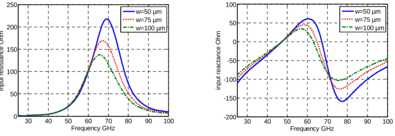
must be matched to the 50 Ohms by varying the length and width for a given substrate. The length and the width affect respectively the resonant frequency, and the resistance of the impedance (Rin). The value of Rin is degraded due to high resistivity of the SOI substrate. For example, for a dipole of length =1250 µm and width=50 µm, the imaginary part of the input resistance shows two different resonant frequencies, a series resonant (47 GHZ) and a parallel resonance (67 GHz) where Rin is equal to 15 Ohms and 215 Ohms respectively. Electromagnetic simulations confirm that increasing the width of the dipole decrease its input resistance. In figure 2 we can see that by increasing the width from 40 to 100 µm, Rin falls from 215 to 137 Ohms. In the same time, the resonant frequency is shifted toward the low frequencies.
30 40 50 60 70 80 90 100 0 50 100 150 200 250 Frequency GHz In p u t re s is ta n c e O h m w=50 µm w=75 µm w=100 µm
III INTERDIGITATED DIPOLE ANTENNA
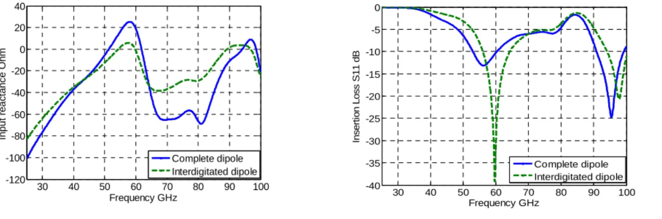
The input impedance of the half wavelength dipole at the fundamental resonance frequency can be modelled as inductance and a capacitance between the arms of the dipole. To compensate the substrate effect on the input impedance, a combination of techniques is directly implemented inside the dipole structure. In the first step, the arms’ width is increased to reduce the quality factor of resonance and obtain a wider operating bandwidth; in the second step, we take advantage of wide arms dipole to introduce an interdigitated structure [6] in order to mainly decrease the imaginary part of its input impedance.
In addition to decrease the input reactance of the antenna, this interdigitated structure affects also its input resistance. A matching with the 50 ohms feed then occurs and consequently a low insertion loss is obtained (figure 5).
The final 60 GHz fully integrated dipole antenna incorporating the interdigitated capacitor is realized on 0.13 µm silicon on insulator (SOI) process, with following parameters : Dipole’s length = 742 µm, width = 100 µm, width of the inter digit =6.25 µm. The arms of the dipole were hollowed out for technological
2-a Input resistance 2-b Input reactance Figure 2: Sweep of the width of the dipole antenna with L=1250 µm
30 40 50 60 70 80 90 100 -200 -150 -100 -50 0 50 100 Frequency GHz in p u t re a c ta n c e O h m w=50 µm w=75 µm w=100 µm
-20 -10 0 10 +90° +60° +30° 0° -30° -60° -90° -120° -150° +180° +150° +120° Antenna Gain at 60 GHz Without reflector With reflector
reasons, and simulations’ results show that insertion loss was not affected. Figure 5-b shows a return loss of – 35 dB at 60GHz with a bandwidth of 10% 30 40 50 60 70 80 90 100 -120 -100 -80 -60 -40 -20 0 20 40 Frequency GHz In p u t re a c ta n c e O h m Complete dipole Interdigitated dipole
The radiation pattern of the integrated dipole shows that the radiation is mainly directed toward the SOI substrate, where losses occur.
The backside metallization under the wafer can be advantageously used to act as a reflector. The radiation pattern is directed outward of the substrate when backside metallization is added. The distance between antenna and the back side metallization (
λ
g4
) is close to the optimal distance in order to add direct and reflected wave without any side lobes [5]. The efficiency of radiation is increased and it is equal to 90 % (simulated results) with a gain around 4.45 dBi (Figure 6). The dipole impedance is equally altered and the resonance is slightly shifted, requiring an additional optimization of the dipole length.IV CPW-CPSTRANSITIONFORCPSDIPOLEANTENNA
Coplanar waveguide (CPW) is widely used for antennas feeding [4]. A balun is inserted between the CPW feed line and the coplanar strip (CPS) input of the dipole antenna for optimal design [1]-[4].The CPW to CPS balun was designed to transform the unbalanced CPW feed line to a balanced CPS feed line [4], [7]. The balun is composed of a radial slot in the terminated ground, and 2 underpasses connecting the 2 ground planes (Figure 6). The characteristic impedance Zc of CPW and CPS TL is firstly calculated by applying the conformal mapping theory [8], but dielectric losses are not taken into account. Another method is to extract the characteristic impedance from electromagnetic simulation. In fact, S parameters of the CPW and CPS are evaluated with respect to reference impedance and the characteristic impedance Zc is calculated [9] using the following equation:
(
) (
)
(
11) (
22)
12 21 21 12 22 111
1
1
1
S
S
S
S
S
S
S
S
Z
Z
c reference⋅
−
−
⋅
−
⋅
−
+
⋅
+
=
In our design, the width of the central strip (w) of the 50 ohms CPW TL is 52 µm and the gap between central and ground plane strip is 20 µm. For the CPS, the gap is 10 and the width of the coplanar strip is 71µm.
The balun structure shown in the figure 4 was fabricated on the M6 copper layer of the SOI substrate, the underpass placed on the stacked M1-M2 layer are connected by via.
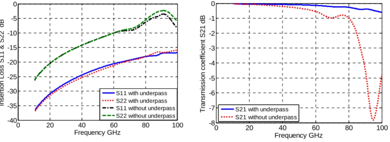
Simulation has proved the importance of the underpass in the design: the reflection coefficient is better than 10 dB where we have about -10 dB without the underpass (Figure 7).
5-a Input reactance of dipole 5-b Insertion Loss of dipole Figure 2 effect of interdigitated structure on dipole performance
Figure 6: gain pattern with and without reflector 30 40 50 60 70 80 90 100 -40 -35 -30 -25 -20 -15 -10 -5 0 Frequency GHz In s e rt io n L o s s S 1 1 d B Complete dipole Interdigitated dipole dBi y z
Figure 7 : parameters of the balun
Similar study has been realised and proved that the radial slot has more advantage with respect to rectangular slot in term of insertion loss and reflection coefficient [4].
Finally, the balun is completely characterized on SOI substrate for subsequent de-embedding of the antenna impedance. 0 20 40 60 80 100 -40 -35 -30 -25 -20 -15 -10 -5 0 Frequency GHz In s e rt io n L o s s S 1 1 & S 2 2 d B S11 with underpass S22 with underpass S11 without underpass S22 without underpass
The effects of pads, balun, and CPW and CPS lines are removed by using a de-embedding procedure of [5] [6]. The procedure is illustrated as follows:
[ ]
Y
Dipole=
[
Y
mesuré]
−
[
Y
(pad,balun,cpw,cps]
The Y matrices of the pad and balun are obtained from S parameters. Subtracting these matrices from the Y matrices of the whole device (pad, dipole and balun) yields to the Y matrices of the dipole alone. The input impedance of the dipole is then found.
These results demonstrate the feasibility of antenna on CMOS SOI technology at 60 GHz for which a bandwidth of 10% at 60 GHz is then observed.
VCONCLUSION
This paper has presented a new architecture of the half wavelength dipole antenna. A 60 GHz fully integrated antenna with an interdigitated structure, is designed at 60 GHz and exhibit an excellent impedance matching to feed line impedance over a wide frequency band.
Antenna feeding is characterized and a balun assuring the transition between the CPW input feed and CPS input antenna is modelled. The back side metallization under the wafer is used to act as a reflector. The radiation pattern is directed outward of the substrate. The efficiency of radiation is equal to 90% with a gain around 4.45 dBi. This antenna is a part of on chip design using CMOS SOI technology in order to be used in the co-design process of the antenna with a 60 GHz integrated Low Noise Amplifier. Experimental results are expected to be available for the conference to confirm simulated results.
REFERENCES
[1] N.Segura , S Montusclat , C. Person , S.Tedjini , D. Gloria, “On-wafer radiation pattern measurements of integrated antennas on standard BiCMOS and Glass processes for 40-80 GHz application”. IEEE Int. Conference on Microelectronic Test Structures, Vol.18, April 2005.
[2] D. Corson and P. Delatte, “Why all the buzz about SOI?” www.rfdesign.com.
[3] J. ,C. Schwartzlow and G. Ponchak, “A Folded Slot Antenna on Low Resistivity Si Substrate with a polymide Interface Layer For Wireless Circuits”. (a revoir le source )
[4] J. Thaysen et al. “Characterisation and optimisation of a coplanar waveguide fed logarithmic spiral antenna,”, Antennas and Propagation for Wireless Communications, 2000 IEEE-APS Conference on ,6-8 Nov. 2000 Page(s):25 - 28.
[5] Constantine A. Balanis, “Antenna theory analysis and design”, p. 453, second edition, John Wiley and Sons, Inc, 1997.
[6] R. Esfandriari, “Design of Interdigitated Capacitors and Their Application to Gallium Arsenide Monolithic Filters”, IEEE Transactions on Microwave Theory and Techniques, Vol.31, NO. 1, January 1983.
[7] Y.M. Li, K. Tilley, J. McCleary, and K. Chang,“Broadband coplanar waveguide-coplanar strip-fed spiral antenna,” Electronic Letters, Vol. 30, pp. 176–177,1995.
[8] Brian C. Wadell, “Transmission Line Design Handbook”, p.79, p.83, Artech House, Inc, 1991.
[9] W. R. Eisenstadt, Y. Eo, “S-paramater-based IC interconnect transmission line characterization”, IEEE transactions on component, hybrids, and manufacturing technology,Vol. 15, No. 4, August 1992.
[10] CST Microwave Studio software 2006 package,http://www.cst.com
0 20 40 60 80 100 -8 -7 -6 -5 -4 -3 -2 -1 0 Frequency GHz T ra n s m is s io n c o e ff ic ie n t S 2 1 d B S21 with underpass S21 without underpass
![[PDF] Tutoriel de Oracle PL/SQL en pdf | cours informatique](data:image/gif;base64,R0lGODlhAQABAIAAAP///wAAACH5BAEAAAAALAAAAAABAAEAAAICRAEAOw==)