Publisher’s version / Version de l'éditeur:
Optics Express, 25, 26, pp. 33018-33028, 2017-12-19
READ THESE TERMS AND CONDITIONS CAREFULLY BEFORE USING THIS WEBSITE.
https://nrc-publications.canada.ca/eng/copyright
Vous avez des questions? Nous pouvons vous aider. Pour communiquer directement avec un auteur, consultez la première page de la revue dans laquelle son article a été publié afin de trouver ses coordonnées. Si vous n’arrivez pas à les repérer, communiquez avec nous à [email protected].
Questions? Contact the NRC Publications Archive team at
[email protected]. If you wish to email the authors directly, please see the first page of the publication for their contact information.
This publication could be one of several versions: author’s original, accepted manuscript or the publisher’s version. / La version de cette publication peut être l’une des suivantes : la version prépublication de l’auteur, la version acceptée du manuscrit ou la version de l’éditeur.
For the publisher’s version, please access the DOI link below./ Pour consulter la version de l’éditeur, utilisez le lien DOI ci-dessous.
https://doi.org/10.1364/OE.25.033018
Access and use of this website and the material on it are subject to the Terms and Conditions set forth at
Athermal planar-waveguide Fourier-transform spectrometer for
methane detection
Podmore, Hugh; Scott, Alan; Cheben, Pavel; Sioris, Chris; Cameron, Peter;
Schmid, Jens H.; Schmid, Jens H.; Lohmann, Andrew; Corriveau, Zachary;
Lee, Regina
https://publications-cnrc.canada.ca/fra/droits
L’accès à ce site Web et l’utilisation de son contenu sont assujettis aux conditions présentées dans le site LISEZ CES CONDITIONS ATTENTIVEMENT AVANT D’UTILISER CE SITE WEB.
NRC Publications Record / Notice d'Archives des publications de CNRC:
https://nrc-publications.canada.ca/eng/view/object/?id=0b0c5355-57a5-42d9-882a-94494996cf27 https://publications-cnrc.canada.ca/fra/voir/objet/?id=0b0c5355-57a5-42d9-882a-94494996cf27Athermal planar-waveguide Fourier-transform
spectrometer for methane detection
H
UGHP
ODMORE,
1,2,*A
LANS
COTT,
2P
AVELC
HEBEN,
3C
HRISS
IORIS,
1P
ETERC
AMERON,
2J
ENSH. S
CHMID,
3A
NDREWL
OHMANN,
1Z
ACHARYC
ORRIVEAU,
1 ANDR
EGINAL
EE1 1Department of Physics and Astronomy, York University, 4700 Keele St, Toronto, ON, Canada 2Honeywell Aerospace, 303 Terry Fox Dr, Kanata, ON, Canada3National Research Council Canada, 1200 Montreal Rd, Ottawa, ON, Canada
Abstract: We demonstrate a passively thermally-stabilized planar waveguide Fourier-transform
spectrometer for remote detection of atmospheric methane. The device is implemented as a spatial heterodyne spectrometer using an array of 100 Mach-Zehnder interferometers (MZIs) on an integrated photonic chip. The spectrometer is buffered against temperature fluctuations by using waveguides with a carefully engineered, athermal geometry. The achieved waveguide thermooptic optic coefficient is 3.5 × 10⁻⁶K−1. Effective entrance aperture is increased over dispersive element spectrometers, without sacrificing spectral resolution, by coupling light independently to each of the 100 MZIs. The output of each MZI is sampled in quadrature, to compensate for non-uniform illumination across the MZI input apertures. The spectrometer is validated using a methane reference cell in a benchtop setup: an interferogram is inverted via least-squares spectral analysis (LSSA) to retrieve multiple absorption lines at a spectral resolution of 50 pm over a 1 nm free spectral range (FSR) centered at λ0= 1666.5 nm. The retrieved spectrum is compared against the Beer-Lambert absorption law and is found to provide a correct measurement of the volume mixing ratio (VMR) in the optical path.
© 2017 Optical Society of America under the terms of theOSA Open Access Publishing Agreement
OCIS codes: (130.0130) Integrated optics; (070.2025) Discrete optical signal processing; (120.6200) Spectrometers
and spectroscopic instrumentation; (300.6310) Spectroscopy, heterodyne; (300.6300) Spectroscopy, Fourier transforms; (350.4238) Nanophotonics and photonic crystals.
References and links
1. D. T. Shindell, G. Faluvegi, D. M. Koch, G. A. Schmidt, N. Unger, and S. E. Bauer, “Improved Attribution of Climate Forcing to Emissions,” Science, 326(5953), 716– 718 (2009).
2. R. W. Howarth, R. Santoro, and A. Ingraffea, “Methane and the greenhouse-gas footprint of natural gas from shale formations,” Clim. Change, 106(4), 679 (2011).
3. S. Kirschke, P. Bousquet, P. Ciais, M. Saunois, J. G. Canadell, E. J. Dlugokencky, P. Bergamaschi, D. Bergmann, D. R. Blake, L. Bruhwiler, P. Cameron-Smith, S. Castaldi, F. Chevallier, L. Feng, A. Fraser, M. Heimann, E. L. Hodson, S. Houweling, B. Josse, P. J. Fraser, P. B. Krummel, J.-F. Lamarque, R. L. Langenfelds, C. Le Quere, V. Naik, S. O’Doherty, P. I. Palmer, I. Pison, D. Plummer, B. Poulter, R. G. Prinn, M. Rigby, B. Ringeval, M. Santini, M. Schmidt, D. T. Shindell, I. J. Simpson, R. Spahni, L. P. Steele, S. A. Strode, K. Sudo, S. Szopa, G. R. van der Werf, A. Voulgarakis, M. van Weele, R. F. Weiss, J. E. Williams, and G. Zeng, “Three decades of global methane sources and sinks,” Nat. Geosci. 6(10), 813–823 (2013).
4. R. Harig, G. Matz, P. Rusch, J.-H. Gerhard, K. P. Schaefer, C. Jahn, P. Schwengler, and A. Beil, “Remote detection of methane by infrared spectrometry for airborne pipeline surveillance: first results of ground-based measurements,” Proc. SPIE 5235, 435–446 (2004).
5. A. Scott, N. Rowlands, and A. Bell, “Miniature Spectrometers for Planetary Remote Sensing,” Proc. SPIE 5660(613), 78–87 (2004).
6. P. Jacquinot, “The Luminosity of Spectrometers with Prisms, Gratings, or Fabry-Perot Etalons,” J. Opt. Soc. Am.
44(10), 761–765 (1954).
7. A. E. Bourassa, J. Langille, B. Solheim, D. Degenstein, and F. Dupont, “The Spatial Heterodyne Observations of Water (SHOW) Instrument for High Resolution Profiling in the Upper Troposphere and Lower Stratosphere,” in
Light, Energy and the Environment, Optical Society of America (2016), paper FM3E.1.
#309752 https://doi.org/10.1364/OE.25.033018
8. P. Cheben, “Wavelength Dispersive Planar Waveguide Devices: Echelle and Arrayed Waveguide Gratings,” in Optical
Waveguides: From Theory to Applied Technologies, M. L. Calvo and V. Lakshminarayanan, eds. (CRC, 2007). 9. P. Cheben, J. H. Schmid, A. Delâge, A. Densmore, S. Janz, B. Lamontagne, J. Lapointe, E. Post, P. Waldron, and
D.-X. Xu, “A high-resolution silicon-on-insulator arrayed waveguide grating microspectrometer with sub-micrometer aperture waveguides,” Opt. Express, 15(5), 2299–2306, 2007.
10. P. Cheben, I. Powell, S. Janz, and D.-X. Xu, “Wavelength-dispersive device based on a Fourier-transform Michelson-type arrayed waveguide grating,” Opt. Lett. 30(14), 1824–1826 (2005).
11. H. Podmore, A. Scott, P. Cheben, A. V. Velasco, J. H. Schmid, M. Vachon, and R. Lee, “Demonstration of a compressive-sensing Fourier-transform on-chip spectrometer,” Opt. Lett., 42(7), 1440–1443 (2017).
12. A. V. Velasco, P. Cheben, P. J. Bock, A. Delâge, J. H. Schmid, J. Lapointe, S. Janz, M. L. Calvo, D.-X. Xu, M. Florjańczyk, and M. Vachon, “High-resolution Fourier-transform spectrometer chip with microphotonic silicon spiral waveguides,” Opt. Lett., 38(5), 706–708 (2013).
13. M. Yang, M. Li, and J.-J. He, “Static FT imaging spectrometer based on a modified waveguide MZI array,” Opt. Lett., 42(14), 2675–2678 (2017).
14. M. Florjańczyk, P. Cheben, S. Janz, A. Scott, B. Solheim, and D.-X. Xu, “Multiaperture planar waveguide spectrometer formed by arrayed Mach-Zehnder interferometers,” Opt. Express, 15(26), 18176–18189 (2007).
15. A. V. Velasco, P. Cheben, M. Florjańczyk, M. L. Calvo, “Spatial Heterodyne Fourier-Transform Waveguide Spectrometers,” in Progress in Optics, Emil Wolf, ed. (Elsevier, 2014).
16. D. A. Naylor, T. R. Fulton, P. W. Davis, I. M. Chapman, B. G. Gom, L. D. Spencer, J. V. Lindner, N. E. Nelson-Fitzpatrick, M. K. Tahic, and G. R. Davis, “Data processing pipeline for a time-sampled imaging Fourier transform spectrometer”, Proc. SPIE 5546, 61–72 (2004).
17. A. Herrero-Bermello, A. V. Velasco, H. Podmore, P. Cheben, J. H. Schmid, S. Janz, M. L. Calvo, D.-X. Xu, A. Scott, and P. Corredera, “Temperature dependence mitigation in stationary Fourier-transform on-chip spectrometers,” Opt. Lett., 42(11), 2239–2242 (2017).
18. J. H. Schmid, M. Ibrahim, P. Cheben, J. Lapointe, S. Janz, P. J. Bock, A. Densmore, B. Lamontagne, R. Ma, W. N. Ye, and D.-X. Xu, “Temperature-independent silicon subwavelength grating waveguides,” Opt. Lett., 36(11), 2110–2112 (2011).
19. P. Vaníček, “Approximate spectral analysis by least-squares fit,” Astrophys. Space Sci. 4(4), 387–391 (1969). 20. L. S. Rothman, I. E. Gordon, Y. Babikov, A. Barbe, D. Chris Benner, P. F. Bernath, M. Birk, L. Bizzocchi, V. Boudon,
L. R. Brown, A. Campargue, K. Chance, E. A. Cohen, L. H. Coudert, V. M. Devi, B. J. Drouin, A. Fayt, J.-M. Flaud, R. R. Gamache, J. J. Harrison, J.-M. Hartmann, C. Hill, J. T. Hodges, D. Jacquemart, A. Jolly, J. Lamouroux, R. J. Le Roy, G. Li, D. A. Long, O. M. Lyulin, C. J. Mackie, S. T. Massie, S. Mikhailenko, H. S. P. Müller, O. V. Naumenko, A. V. Nikitin, J. Orphal, V. Perevalov, A. Perrin, E. R. Polovtseva, C. Richard, M. A. H. Smith, E. Starikova, K. Sung, S. Tashkun, J. Tennyson, G. C. Toon, V. G. Tyuterev, and G. Wagner, “The HITRAN2012 molecular spectroscopic database,” J. Quant. Spectrosc. Radiat. Transfer 130, 4–50 (2013).
1. Introduction
Methane is a greenhouse gas that contributes significantly to global climate change through its absorption of outgoing infrared (IR) radiation and interaction with atmospheric aerosols [1]. Methane is increasingly recognized as a significant but poorly-monitored contributor to global climate change [2]. Consequently, there exists a recognized need to develop new methods to accu-rately evaluate the global methane distribution. Many high-density sources of methane emission (fracking sites, pipelines, mines, agribusiness, etc.) have been identified, however monitoring these sites remains a technical challenge due to their extensive geographic distribution [2, 3].
One promising technique for inexpensively monitoring sparsely distributed sources of methane is remote detection of atmospheric methane via observation of molecular absorption lines using high-resolution IR spectrometers [4]. Such spectrometers may be housed on highly mobile platforms such as unmanned aerial vehicles (UAVs), and micro and nanosatellites in order to provide global coverage of methane emission sources. A key technological challenge to utilizing these platforms lies in the development of small, low-mass spectrometers with sufficient spectral resolution to distinguish molecular absorption lines separated by tens of picometers [5].
High-resolution spectrometers usually fall into one of two categories: dispersive element spectrometers, and Fourier-transform spectrometers (FTS). Of these two, FTS devices, in which the input light undergoes sinusoidal modulation via self-interference, are preferred for their throughput advantage in high-resolution applications (the Jacquinot advantage [6]). FTS instruments designed as spatial heterodyne Fourier-transform spectrometers (SHFTS) are well
suited to remote-sensing from aircraft as they may be implemented as a monolithic glass block with no moving parts [7]. In an SHFTS, light is spectrally dispersed and recombined to produce a spatially-modulated interference pattern that may be read out using an array of detectors. SHFTS devices achieve high spectral resolution at the expense of bandwidth, which limits their utility for simultaneous detection of multiple atmospheric species. Ultimately, the integration of SHFTS devices onto small mobile platforms may be limited by the size and mass of the monolithic interferometer.
One promising avenue for miniaturization of high-resolution spectrometers lies in planar waveguide photonic chip technology [8]. Waveguides can be fabricated on silicon substrates in high-density arrangements, enabling the integration of complex optical circuits, including SHFTS, into centimeter-sized chips, or smaller [9].
The first on-chip SHFTS was proposed in Michelson configuration [10] and was subsequently implemented as an array of MZIs with linearly increasing optical path delays (OPDs) [11–15]. These MZIs constitute a discrete Fourier-transform in which the output of each MZI corresponds to a point in the spatial interferogram. These points may be sampled independently via photodiodes placed on the chip or by an external linear detector array. The interferogram may then be inverted using the fast Fourier-transform (FFT) to retrieve the input spectrum. The simultaneous spatial sampling scheme in an SHFTS allows for instantaneous acquisition of an interferogram in a single shot, unlike a scanning FTS where the interferogram is collected over time. Single-shot acquisition enables signal enhancement through extended exposure, as well as observation at high readout rates—suitable, for example, for fast-moving satellites. The small size of these chips may also enable the detection of multiple atmospheric species from a single integrated platform using vertically stacked on-chip spectrometers, each designed for a separate atmospheric species. One challenge yet to be addressed in the implementation of planar waveguide SHFTS technology lies in compensation for rapid thermal drifts, which result in non-uniform sampling of the interferogram. Spectral inversion of an interferogram via the FFT requires the sampling locations to be evenly separated, i.e. each OPD must be an exact integer multiple of the first [16]. In regular operation, however, the OPDs will vary due to imperfections introduced during the fabrication process as well as fluctuations in chip temperature. As with many dispersive materials, planar waveguides experience temperature-dependent shifts in their refractive index which may be significant over long optical distances. Therefore, thermal compensation in SHFTS devices is of critical importance [17].
In this paper we present a miniaturized high-resolution planar waveguide SHFTS for methane detection with many innovative aspects. We use passive thermal stabilization of the device— achieved through waveguide refractive index engineering—to stabilize the interferogram and reduce temperature sensitivity. We use a multi-aperture input array to maximize optical throughput, and sample MZI outputs in quadrature to compensate for irregular input coupling. Finally, we use the waveguide SHFTS and a reference gas cell to demonstrate on-chip SHFTS detection of atmospheric absorption features for the first time.
2. Theory and simulation
Our SHFTS device is designed to target the Q-branch absorption features of methane, consisting of strong, closely-spaced molecular lines covering a spectral range of 2.2 nm centered at λ0= 1666.3 nm. The Q-branch features are selected for this experiment as they do not overlap with other atmospheric species; however, in principle, any atmospheric species may be selected. The planar waveguide spectrometer is formed by 100 unbalanced MZIs arrayed in a high-density configuration on a single chip. Our device targets a spectral resolution of δλ = 0.050 nm and bandwidth of ∆λ = 2.5 nm in order to resolve multiple absorption features within the Q-branch. The OPDs of the longest and shortest MZIs set the resolution (δσ) and bandwidth (∆σ) in wavenumbers as δσ = 1/(ne f f∆Lmax), and ∆σ = 1/(2ne f f∆L). In our device ∆L = 0.0326 cm
xn = neff n∆L x3 = neff 3∆L ... Pin(σ) Ithru Icross σ Icross Ithru Ii (σ) 0
∫
P( x x1 x0 x2 x3 xn I(x) ... ... x2 = neff 2∆L x1 = neff 1∆L x0 = neff 0∆LFig. 1. Diagram showing the operating principle for an on-chip SHFTS. MZIs are implemented as squared spirals, enabling high-density packing. Each MZI has an independent aperture and splits its outputs into two ports which are 180◦out-of-phase as shown in the lower inset. The continuous interferogram, I(x), is sampled at locations defined by the OPDs of each MZI, as shown in the upper inset.
is the physical path difference of the least unbalanced MZI, ne f f is the effective index of the
waveguide, and ∆Lmax= 3.26 cm is the maximum physical path difference. The OPD of the i-th MZI is then given by xi = ne f fi∆L, as shown in Fig. 1.
The SHFTS device is implemented on a silicon wafer with an 8 µm thick silicon dioxide (SiO2)
layer forming the lower cladding. The waveguide layer consists of two 300 nm thick layers of silicon nitride (Si3N4) separated by a 90 nm layer of strain-relieving SiO2. The upper cladding of
the waveguide structure is formed by a 6 µm layer of SU-8 polymer. This waveguide structure is designed to produce an effective index ne f f = 1.7 at λ0 = 1666.3 nm for the fundamental
transverse electric (TE) mode.
The first innovative aspect of this device is the use of a multi-aperture input scheme coupled with MZI signal normalization. This concept was proposed in [14]; in this paper we demonstrate it experimentally for the first time. Each MZI in our device possesses an independent aperture (input coupler), and splits its interferometric signal between two waveguide outputs to provide signal normalization. Independent input coupling—rather than splitting a single input signal multiple times—increases the optical throughput of each MZI, improving the signal-to-noise ratio (SNR) at the pixel array [13]. In a multi-aperture input scheme, non-uniform illumination of the aperture and input-to-input variations in coupling efficiency may distort the interferogram. Therefore, the interferometric signal of each MZI must be normalized against its input intensity [14].
In our device, splitting and recombining in each MZI is accomplished through the use of 2 × 2 multi-mode interference couplers (MMIs). MMIs are preferred over Y-splitters as MMIs introduce a 90◦relative phase shift between the cross-port and through-port signals; this phase shift may be used as the basis for signal normalization. Light entering the MZI is split at the first MMI where the reference arm (cross-port) receives a +90◦phase delay relative to the delay arm (through-port). When the two arms are joined at the through-port of the second MMI, the delay arm and reference arm will be 180◦out-of-phase in addition to any OPD-induced phase shift. By contrast, at the cross-port of the second MMI, the two arms will each have received a 90◦phase shift from one of the two MMIs and will combine in-phase. This process is shown diagrammatically in Fig. 1. The resulting pair of outputs for the i-th MZI, and the associated
interferogram, may then be described using the following modulation functions: Pthr u(σ, i) = P0(σ) 2 (1 + cos(2πne f fi∆Lσ)) (1) Pcr oss(σ, i) = P0(σ) 2 (1 − cos(2πne f fi∆Lσ)) (2) I(xi) = ∫ P0(σ)cos(2πne f fi∆Lσ)dσ, (3)
where P0(σ) is the optical input power as a function of wavenumber. The through-port and
cross-port signals may be added to retrieve the normalization factor P0 = Pthr u+ Pcr oss, or
subtracted to produce a modulation function, Pthr u− Pcr oss = P0cos(2πne f fi· ∆Lσ). The
normalization factor may then be used to correct for irregular illumination across the input aperture. Such irregularities may be caused by misalignment of the frontend optics, or chip fabrication imperfections including damage to the facet.
The second innovation achieved in this device is to reduce the thermal sensitivity of the SHFTS. Spectral retrieval from a planar waveguide SHFTS relies on accurate knowledge of the OPD for each MZI, however, the OPDs of each MZI may fluctuate with temperature. Thermal drifts may be compensated provided that the temperature of the spectrometer is known to a sufficiently precise degree [17]. In this case, the required level of precision of the temperature measurement will be set by the thermal sensitivity of the chip. The response of each MZI to an uncompensated (i.e. unknown) temperature change of magnitude ∆T may be derived from the change in the phase delay, φ(∆T) = 2πσ(ne f f∆L + d/dT(ne f f∆L)∆T). We collect the temperature dependent terms
into an effective thermooptic coefficient (TOC), αe f f = 1/ne f fdne f f/dT + d/dT(∆L) and write
the MZI response as:
Ii(σ, ∆T) ≈ P0(σ)cos(2πσi∆Lne f f(1 + αe f f∆T)), (4) where αe f f is an equivalent TOC of the waveguide combining the coefficient of thermal
expansion of the substrate, and refractive index changes in the cladding and waveguide material. Equation (4) can be used to evaluate the impact of a particular TOC on the interferometric output, and determine the temperature knowledge required to limit variability in the interferogram to less than 5%. Were the spectrometer to be realized using standard silicon wire waveguides (ne f f = 2.5, ∆Lmax = 2.22 cm), the TOC of silicon (αSi = 1.8E − 4K−1) at the central
wavenumber σ0= 6001cm−1would require that the temperature be monitored to an accuracy of
0.1 mK. In a dynamic environment it is unlikely that such a measurement could be practically achieved. However, if the waveguide TOC is substantially reduced, then temperature measurements may be obtained with less difficulty.
The waveguide geometry, shown in Fig. 2, is designed to passively reduce the equivalent TOC, thereby attenuating the thermal sensitivity (Eq. (4)). The TOC of the effective mode index is engineered by controlling the fraction of modal power that propagates within the SU-8 upper cladding—which has a negative refractive index coefficient—versus the Si3N4core and SiO2lower
cladding [18]. We calculated the equivalent TOC of the mode effective index for the fundamental TE mode by weighted sum of the material coefficients, αe f f = 1/ne f fÍΓici+ d∆L/dT , as described in Table 1. In this sum the optical terms for each material are weighted by their modal power fraction (i.e. the percentage of modal power propagating in the respective medium), and the thermal expansion of the substrate is weighted by the effective index of the waveguide.
For our chosen waveguide materials and core geometry we calculate an expected TOC of αe f f = −2.5 × 10⁻⁶K−1, corresponding to a temperature knowledge requirement of ∆T = 12
Fig. 2. Waveguide cross-section showing modal power distribution and waveguide dimensions. The waveguides are formed on an 8 µm thick layer of SiO2, and the waveguide core consists of two 300 nm thick layers of PECVD Si3N4separated by a 90 nm thick SiO2layer. The upper cladding is formed by a 7 µm thick layer of SU-8 polymer.
Table 1. Thermal coefficients, ci, with associated weighting factors, Γi, and contributions to equivalent TOC, αi.
Material Coefficient (K−1) Weight (Γi) αi (10−6)
SU-8 −1.2 × 10⁻⁴ 0.21 -25.2 Si3N4 2.45 × 10⁻⁵ 0.72 17.6 SiO2 0.95 × 10⁻⁵ 0.07 0.7 d∆L/dT 4.4 × 10⁻⁶ – 4.4
Total -2.5
cladding necessitates a high degree of waveguide core confinement to produce an athermal waveguide: Γcor e= 0.7. In actuality, the core confinement parameters in Table 1 are subject to some uncertainty due to expected variations in the thickness and width of the waveguide core during fabrication. We quantify the effect of this uncertainty by Monte-Carlo analysis: accounting for expected fabrication tolerances (±1% on all cross-section dimensions) the expected upper bound of the TOC is found to be |αe f f| < 5 × 10⁻⁶K−1. This corresponds to a temperature
knowledge requirement of ∆T = 6 mK, a significant improvement over prior implementations of the technology in Si-wire waveguides [17].
3. Experimental results and discussion
The wafers and waveguides were fabricated by LioniX International, and the SU-8 upper-cladding and wafer dicing were performed as a post-process. The lower cladding was formed by a thick thermal oxide layer grown on a Si substrate. The three core waveguide layers were deposited by plasma-enhanced chemical vapour deposition (PECVD), patterned with an i-line stepper and defined by reactive ion etching (RIE). The wafers were further processed at the SU-8 was deposited via spin-coating to form the upper cladding. Finally, the wafers were diced into individual chips at the Toronto Nanofabrication Center. An image of the processed spectrometer chip next to a Canadian 25-cent coin is shown in Fig. 3(c).
We built a benchtop setup to characterize, calibrate, and demonstrate the functionality of the spectrometer chip. Light from a tunable laser source is coupled to a single-mode fiber, and routed
Laser Wavemeter CH4 PD1 PD2 90:10 90:10 PBS Camera LP Chip L2 L1 a. b. c.
Fig. 3. (a) Light from a tunable laser is coupled into a single-mode fiber (yellow), and passes through a 7.5 cm methane cell. The optical power is tapped at 10% and monitored using an InGaAs photodiode (PD1). The single mode fiber is split by a polarizing beam splitter (PBS) into two polarization-maintaining fibers (blue). One arm leaving the PBS is directed to a wavemeter and photodiode (PD2). The second arm is directed to the chip via a fiber collimator and focused in the horizontal and vertical axes by two cylindrical lenses (L1, L2). The output signal is passed through a linear polarizer (LP) and captured by an InGaAs camera. (b) Output signal captured by camera. (c) Photograph of FTS chip next to a 25-cent Canadian coin.
to a polarizing beam splitter (PBS). One arm of the PBS monitors the wavelength and power of the laser output; in the second, light is passed to a fiber collimator directed at the input aperture of the chip. The splitting ratio is monitored by a pair of photodiodes located before and after the PBS. Light from the fiber collimator is focused onto the waveguide facets via two cylindrical lenses placed in front of the aperture of the photonic chip. The output signal passes through a linear polarizer where transverse-magnetic (TM)-polarized light is rejected, and the TE-polarized light is imaged by an IR camera. The experimental setup is shown schematically in Fig. 3(a). The chip itself is placed on a 6-axis mechanical stage and its temperature is controlled by a Peltier module.
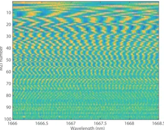
The wavelength of the tunable laser is swept across the operating range of the spectrometer, and the output signals from each MZI are collected. When this procedure is performed with the gas cell removed, and with a laser linewidth substantially less than the SHFTS spectral resolution, the product is an M × N transformation matrix, A, in which M is the number of MZIs, and N is the number of measured wavelength points. In this transformation matrix, also called a spectral (or calibration) map, each row contains the modulation response for a single MZI output as a function of wavelength. The experimental matrix obtained from the methane spectrometer chip is shown in Fig. 4. It can be seen from this matrix that the fringe contrast decreases with increasing OPD; this is an expected consequence of the waveguide propagation loss, which is determined to
1666 1666.5 1667 1667.5 1668 1668.5 Wavelength (nm) 10 20 30 40 50 60 70 80 90 100 MZI number
Fig. 4. Measured calibration matrix of the SHS chip showing the wavelength-dependent response of each of the 100 MZIs obtained during a high-resolution scan over a 2.5 nm bandwidth between 1666 nm and 1668.5 nm. MZIs are ordered sequentially according to their OPDs, with MZI 1 having the shortest OPD and MZI 100 having the longest.
be 2.1 dB/cm.
The tunable laser is used to record the interferogram corresponding to a specific optical bandpass. With the gas cell in the optical path, an interferogram, y, is obtained by performing laser sweeps across a selected spectral range and time-averaging the waveguide outputs (Fig. 3(b)). The spectral range covered by the laser during sampling simulates a flat-topped anti-aliasing bandpass filter. In an operational scenario the bandpass filter would be placed at the telescope input, and a broadband light source (such as the sun) would illuminate the SHFTS. We utilize the tunable laser source to have precise control over the oversampling factor for the interferogram, noting that this may overestimate the coupling efficiency compared to realistic incoherent broadband input. The oversampling factor for a particular bandpass with spectral range ∆λ, and spectral resolution δλ is given by c = Mδλ/(2∆λ), where c = 1 corresponds to critical (Nyquist) sampling. The input spectrum, x, can be retrieved as the FFT of a critically-sampled interferogram, or by non-uniform Fourier-transform (NFFT) of an oversampled interferogram [16, 19]. Without loss of information, the number of spectral points in x is necessarily half the number of MZIs since the FFT requires a solution to both the amplitude and phase of each spectral component.
For this analysis we found that a least-squares spectral analysis (LSSA) using the pseudoinverse of the transformation matrix [11, 17, 19] with an oversampling factor of c = 2.5 provided the best SNR. The pseudoinverse of A is applied to the interferogram, y, to retrieve an estimate, ˆx, of the input spectrum, where y ≈ Ax. This process may be summarized as:
ˆx = (ATA)−1ATy. (5)
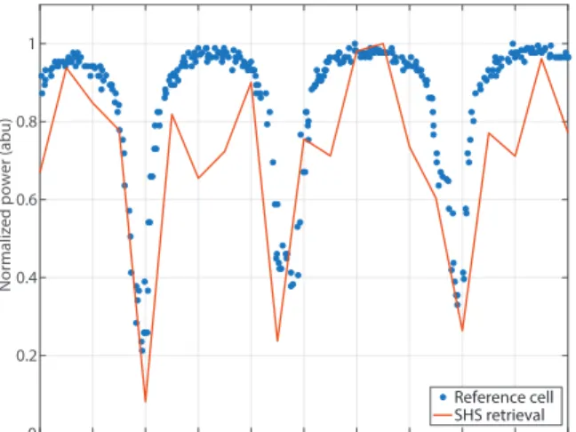
In Fig. 5 we present a retrieval of the methane transmission spectrum obtained from the gas cell by LSSA. The tunable laser source is used to effect a boxcar bandpass filter from 1666 nm to 1667 nm, providing an oversampling factor of c = 2.5. The interferogram is inverted using Eq. (5), where A is the calibration matrix shown in Fig. 4. To obtain an estimate of the methane concentration in the gas-column, the SHS spectrum is fit to a Beer-Lambert absorption model using absorption coefficients obtained from HITRAN [20]. Using SHFTS measurements the
1666 1666.1 1666.2 1666.3 1666.4 1666.5 1666.6 1666.7 1666.8 1666.9 1667 Wavelength (nm) 0 0.2 0.4 0.6 0.8 1
Normalized power (abu)
Reference cell SHS retrieval
Fig. 5. Experimental observation of methane absorption features using on-chip SHFTS over 1 nm bandwidth with 50 pm resolution. The spectrum is obtained from the interferogram via pseudoinverse of the calibration matrix shown in Fig. 4. The signal collected by the reference photodiode (PD1 in Fig. 3(a)) is also displayed. The methane absorption features in the reference cell are retrieved with SNR > 3 : 1.
volume mixing ratio (VMR) along the optical path including the gas reference cell is determined to be 0.40 ± 0.11. For the purpose of comparison, a reference VMR value of 0.370 ± 0.009 is obtained using the high-resolution photodiode signal shown in Fig. 5. The SHFTS and reference values are in agreement, with the reference signal achieving greater precision due to its improved spectral resolution. The precision of the SHFTS retrieval may be improved by increasing the input coupling efficiency of the SHFTS using spot-size converters, surface grating couplers or micro-lens arrays. The precision may be further improved by bringing a linear detector directly to the edge of the chip in order to increase light capture; an SHFTS mated with commercial detectors would achieve 41 dB dynamic range.
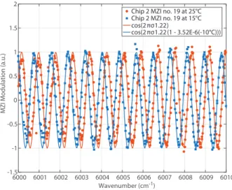
The setup shown in Fig. 3 was also used to characterize the thermal sensitivity of the chips. The TOC of the waveguides is determined using two calibration maps obtained at T1= 25◦C and T2 = 15◦C. The difference in modulation period observed in a single modulation function at T1and at T2is governed by the TOC acting on the OPD. The modulation functions of MZIs with long OPDs—which exhibit greater sensitivity to temperature changes—were measured and used to determine the value of the waveguide TOC by least-squares fitting to Eq. (4). This procedure is shown in Fig. 6. The value obtained from the high-sensitivity MZIs is cross-validated against the response of low-sensitivity MZIs to eliminate the possibility of aliasing (i.e. underestimation due to an apparent 2π shift in the sinusoid). The resulting TOC is αe f f = −3.52 × 10⁻⁶K−1,
corresponding to a temperature knowledge requirement of ∆T < 9 mK. This value agrees with the Monte-Carlo envelope, and represents an order-of-magnitude improvement over uncompensated Si3N4/SiO2 waveguides (αe f f = 2.5 × 10⁻⁵K−1) and a two-order improvement over silicon waveguides (αe f f = 1.8 × 10⁻⁴K−1).
These results demonstrate significant advances in SHFTS on-chip capability. Through passive thermal management we demonstrate that SHFTS devices may be substantially insulated against their environment, enabling SHFTS deployment on low-power miniaturized remote sensing platforms. Secondly, through selective oversampling we demonstrate, for the first time, that SHFTS on-chip technology may be used to retrieve complex, broadband spectra, and that these
6000 6001 6002 6003 6004 6005 6006 6007 6008 6009 6010 Wavenumber (cm-1) -1.5 -1 -0.5 0 0.5 1 1.5 2
MZI Modulation (a.u.)
Chip 2 MZI no. 19 at 25°C Chip 2 MZI no. 19 at 15°C cos(2 πσ1.22)
cos(2 πσ1.22 (1 - 3.52E-6(-10°C)))
Fig. 6. Modulation function of a high-sensitivity MZI as a function of wavenumber at T1= 25 ◦C and T
2 = 15◦C. The modulation function is obtained as the difference in intensity between the two out-of-phase MZI outputs normalized by their sum. The OPD of the device (1.22 cm) is first constrained by a cosine fit to the modulation function at 25◦C. The TOC is then determined by fitting the modulation function at 15◦C (i.e. ∆T = −10◦C) to Eq. (4), yielding the TOC αe f f = −(3.52 ± 0.05) × 10−6K−1.
spectra may be used to correctly predict the column-length of an atmospheric species.
4. Conclusion
In this paper we implement a high-resolution spatially-heterodyned Fourier-transform on-chip spectrometer for remote detection of methane. In doing so, we address a number of outstanding challenges to the realization of miniaturized spectrometers for remote sensing in dynamic environments. Waveguide interferometers are lithographically defined as squared-spirals enabling a high-density layout of 100 interferometers on a device measuring 12 mm by 22 mm. The SHFTS comprises an array of 100 waveguide interferometers with independent input apertures. This design is used to enlarge the total input aperture of our waveguide spectrometer over dispersive-element systems, enhancing optical throughput. High-resolution (50 pm) spectroscopy in the presence of non-uniform spatial sampling of the interferogram is achieved using LSSA over a restricted optical bandwidth of 1 nm. The thermal sensitivity of the waveguide device is substantially moderated through the use of a passively athermal waveguide geometry, enabling the device to operate in a dynamic environment with reduced active thermal compensation. Finally, we use this spectrometer to demonstrate, for the first time, standoff detection of atmospheric absorption features using an on-chip spectrometer. The technical advances presented here extend the capability of the on-chip SHFTS architecture for high resolution spectroscopy, opening the door for future realization and deployment of integrated SHFTS devices on miniaturized remote-sensing platforms in dynamic environments.
Funding
The authors would like to acknowledge the support this work has received from the Canadian Space Agency (CSA), the Natural Sciences and Engineering Research Council of Canada (NSERC), and from Honeywell Aerospace.
Acknowledgments
The authors also acknowledge Robert Halir for his helpful discussions on multimode interference device design, as well as Mohammad Soltani for SU-8 deposition, and Harlan Kuntz for his assistance in wafer dicing. The authors also acknowledge the use of the Giga-to-Nano (G2N) fabrication center at the University of Waterloo, as well as the Toronto Nanofabrication Center (TNFC) at the University of Toronto.