An Analytical Framework for Field Electron
Emission, Incorporating Quant um- Confinement
Effects
by
Alex A.
Patterson
B.S., Electrical Engineering (2011)
University of Pittsburgh
ARcHNf.
MASSACHUSETTS INSTITUTE OF TECH-NOLCLGYL
RRI ES
Submitted to the Department of Electrical Engineering and Computer
Science
in partial fulfillment of the requirements for the degree of
Master of Science
at the
MASSACHUSETTS INSTITUTE OF TECHNOLOGY
September 2013
©
Massachusetts Institute of Technology 2013. All rights reserved.
Author ...
Department of
Certified by...
-
-
I-- -
- -.....
lectrical Engineering and Computer Science
I
A
1July
30, 2013
Akintunde I. Akinwande
Professor of Electrical Engineering and Computer Science
Thesis Supervisor
(-j) . I
Accepted by ...
I
An Analytical Framework for Field Electron Emission,
Incorporating Quantum- Confinement Effects
by
Alex A. Patterson
Submitted to the Department of Electrical Engineering and Computer Science on July 30, 2013, in partial fulfillment of the
requirements for the degree of Master of Science
Abstract
As field electron emitters shrink to nanoscale dimensions, the effects of quantum con-finement of the electron supply and electric field enhancement at the emitter tip play a significant role in determining the emitted current density (ECD). Consequently, the Fowler-Nordheim (FN) equation, which primarily applies to field emission from the planar surface of a bulk metal may not be valid for nanoscale emitters. While much effort has focused on studying emitter tip electrostatics, not much attention has been paid to the consequences of a quantum-confined electron supply. This work builds an analytical framework from which ECD equations for quantum-confined emitters of various geometries and materials can be generated and the effects of quantum con-finement of the electron supply on the ECD can be studied. ECD equations were derived for metal emitters from the elementary model and for silicon emitters via a more physically-complete version of the elementary model.
In the absence of field enhancement at the emitter tip, decreasing an emitter's dimensions is found to decrease the total ECD. When the effects of field enhancement are incorporated, the ECD increases with decreasing transverse emitter dimensions until a critical dimension dpeak, below which the reduced electron supply becomes the limiting factor for emission and the ECD decreases. Based on the forms of the ECD equations, alternate analytical methods to Fowler-Nordheim plots are introduced for parameter extraction from experimental field emission data. Analysis shows that the
FN equation and standard analysis procedures overpredict the ECD from
quantum-confined emitters. As a result, the ECD equations and methods introduced in this thesis are intended to replace the Fowler-Nordheim equation and related analysis procedures when treating field emission from suitably small field electron emitters.
Thesis Supervisor: Akintunde I. Akinwande
Acknowledgments
There are many people who have played an important role in me completing this work and I would like to thank them below. For those whom I may not have mentioned, thanks go out to you as well.
First, I'd like to thank my advisor, Professor Tayo Akinwande, for his guidance, encouragement, and support during this work. I could not possibly enumerate either the lessons I have learned or the great advice he has given me in the first two years of my graduate education. He holds his students to the highest scientific standards, making sure that they conduct their research carefully and completely, and from this
I have grown immensely as a researcher and student. I appreciate that he has given
me so much freedom in choosing the work I want to pursue, but also bringing me back to Earth when I need it. From him I have also learned that my work is only as good as my ability to convey it to others, whether it be placing it within the big picture or organizing my research into a compelling narrative. His enthusiasm for research and education is infectious and has served as a continuing motivation in my own career.
I would also like to thank the members of the Akinwande group: Melissa Smith, Steve Guerrera, and Arash Fomani, who have made this work and my experience as a graduate student go much more smoothly than it probably should have. They have answered my incessant questions about graduate school, served as a sounding board for my research ideas, and given me solid advice on so many topics. From discussions in the office to spending some quality time at the library, my group-mates have made life in building 39 truly a great experience.
Finally, I would like to thank my mom, dad, and brother for making sure that I take time to enjoy life outside my work and providing comic relief and reassurance when I needed it; Dan for his encouragement, commiseration as a fellow graduate student, and discussions about the elegance of physics and mathematics; Cait for her continued support and advice on life in general; the Exit Row Bros for keeping the graduate student life in (and outside of) Cambridge fun and continually interesting; Dr. David "Degas" Perello, Mike Rogers, and the members of Degas for ensuring that I don't forget about the importance of all my other major interests.
Contents
1 Introduction 21
2 Background 25
2.1 Fowler-Nordheim Equation . . . . 25
2.2 Fowler-Nordheim-Type Equations . . . . 31
2.2.1 Temperature Correction Factor: AT . . . . 32
2.2.2 Band Structure Correction Factor: AB . . . . 32
2.2.3 Field Enhancement Factor: . . . .. 37
2.2.4 Tunneling Prefactor and Correction Factor: P and Ap . . . . . 38
2.2.5 Barrier Shape and Decay Width Correction Factors: v and A, 40 2.3 Emission from Semiconductors . . . . 40
2.3.1 Emission from the Conduction Band for EF > 0 . . . . . . . . 41
2.3.2 Emission from the Conduction Band for EF < 0 . .. . . . 44
2.3.3 Emission from the Valence Band for EF, < 0 . . . . 46
2.3.4 Field Penetration and Band Bending . . . . 49
2.3.5 Tunneling from an Accumulation Layer . . . . 51
2.4 Emission from Quantum-Confined Emitters . . . . 53
2.4.1 Emission from a Nanowall Edge . . . . 53
2.4.2 Emission from a Thin Slab . . . . 57
3 Elementary Framework for Cold Field Emission from Metal Emit-ters
3.1 Introduction . . . .
3.2 Model for Field Emission from Quantum-Confined Emitters . . . . . 3.2.1 Definition of Emitter System ...
3.2.2 Quantum Confinement of Electrons . . . .
3.3 Construction of the Framework . . . .
3.3.1 Emitted Current Density . . . .
3.3.2 Supply Functions . . . .
3.3.3 Transmission Function . . . . 3.4 Application of the Elementary Framework: Emitted Current Density
E quations . . . . 3.4.1 Normally-Unconfined Emitted Current Density Equations . .
3.4.2 Normally-Confined Emitted Current Density Equations . . . . 3.5 Chapter Summ ary . . . .
4 Treatment of Field Emission from Quantum-Confined Silicon Emit-ters
4.1 Introduction . . . . 4.2 Correction Factors: Emitter Electrostatics . . . . 4.2.1 Schottky-Nordheim Barrier for Semiconductors . . . .
4.3 Correction Factors: Emitter Electron Supply for Silicon . . . . 4.3.1 Material Properties of Silicon . . . . 4.3.2 Band Structure Corrections for QC Emitters . . . . 4.4 Emitted Current Density Equations for Silicon . . . .
4.4.1 ECD Equations: Conduction Band EF > 0 . . . . . . .. . .
4.4.2 ECD Equations: Conduction Band EF < 0 . . . . . . .
4.5 Chapter Sum m ary . . . . 61 61 62 62 62 68 68 68 71 76 77 81 84 85 85 86 86 87 87 88 92 94 101 106
5 Analysis of the Emitted Current Density from Quantum-Confined
Emitters 109
5.1 Introduction . . . . 109
5.2 ECD as a Function of Emitter Dimensions: Elementary Model . . . . 110
5.2.1 Effects of Transverse Quantum Confinement . . . ..110
5.2.2 Normal Quantum Confinement . . . . 113
5.3 ECD as a Function of the Quantum Well Width: Silicon ECD Equations117 5.3.1 Finite Temperature . . . . 117
5.3.2 Schottky-Nordheim Barrier . . . . 118
5.3.3 Band Structure Effects . . . . 119
5.4 Fowler-Nordheim Plots for Quantum-Confined Emitters . . . . 123
5.4.1 Parameter Extraction from Normally-Unconfined Emitters . . 123
5.4.2 N C Em itters . . . . 127
5.5 Comparison of Framework Equations to Experimental Data . . . . . 128
5.5.1 Vertical Single-Layer Graphene . . . . 128
5.5.2 Single-Walled Carbon Nanotube . . . . 130
5.6 Chapter Summ ary . . . . 131
6 Thesis Summary and Future Work 135 6.1 Sum m ary . . . . 135
6.2 M odel Lim itations . . . . 137
6.3 Future W ork . . . . 139
A Poisson-Boltzmann Formulation of Band Bending 153 B Elementary Emitted Current Density Equations 157 B.1 Normally-Unconfined Emitted Current Density Equations . . . . 157
B.1.1 NU Nanowire . . . . 157
B.2.1 NC Nanowall ... .. ...
B.2.2 NC Rectangular Nanowire . . . .
B.2.3 NC Cylindrical Nanowire . . . .
C Field Enhancement Factor
C.1 Floating Sphere at Emitter Plane Potential ...
C.2 Semicylinder on Emitter Plane . . . . C.3 Floating Cylinder at Emitter Plane Potential . . . .
D Emission from an Accumulation Layer
D.1 Accumulation Layer Well . . . . D.2 Accumulation Layer Emitted Current Density . . . .
E Transition Region Between Emitter Dimensionalities E.1 Transition Point . . . . E.2 Transition Region and the Influence of System Parameters
E.2.1 Work Function . . . .
E.2.2 Effective Mass of Electrons . . . .. . . . E.2.3 Applied Electric Field . . . .
E.2.4 Fermi Energy . . . .
175 . . . . 175 . . . . 176 . . . . 177 . . . . 178 . . . . 179 . . . . 179 158 158 159 161 161 162 164 167 167 172
List of Figures
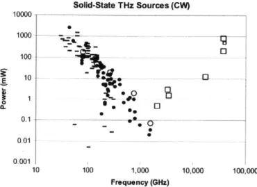
1-1 A plot of the output power vs. operating frequency of state-of-the-art
continuous-wave terahertz sources shows a lack of devices with power
outputs of 1 W or greater between approximately 100 GHz and 10
THz. QCLs are represented by (s), frequency multipliers by (e) and other electronic devices by (-). Cryogenic results are plotted as hollow sym bols. . . . . 22
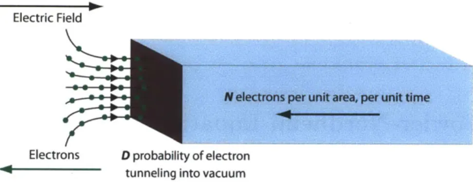
2-1 Field emission consists of electrons being emitted from a material that
has an electric field applied to one of its surfaces. The magnitude of the
emitted current density depends on the electron flux at the surface of
the emitter and the probability of electrons tunneling from the material
into vacuum . . . . . 26
2-2 Normal energy diagram for a bulk metal emitter. As W increases, the
barrier height seen by tunneling electrons decreases. . . . . 28
2-3 Fowler-Nordheim plot for an emitter with q = 5 eV. The linear fit
y-intercept is equal to A and the slope is -B 3/2. . . . . 29
2-4 Normal energy diagram for a bulk emitter with the Schottky-Nordheim
barrier potential. . . . . 29
2-5 An example of a constant energy surface. This constant energy surface
is being projected into the k,-k. plane, which is perpendicular to the
2-6 (a) Ellipsoidal constant energy surface with mo > m, > mz = my
(blue) compared to the free electron constant energy surface (red), (b)
ellipsoidal and free electron constant energy surfaces projected into
the k, - ky plane, and (c) ellipsoidal and free electron constant energy
surfaces projected into the k, - k, plane. . . . . 34
2-7 Actual and free electron constant energy surfaces projected into the
E,-Ey plane. The area inside the red (blue) contour represents electron
states that contribute to the free electron (actual) ECD. Areas shaded
gray (orange) are electron states that contribute to the actual (free
electron) ECD, but are excluded by the free electron (actual) ECD. If
the constant energy surface has a neck, it is projected as an absence
of electronic states in the E,-Ey plane and therefore is also shaded
orange. Figure adapted from [1] . . . . . 36
2-8 A schematic for the "floating sphere at emitter plane potential" model.
The center of the sphere of radius p is located a distance 1 above the
emitter plane. Far away from the sphere, the electric field is FM, while
at the apex of the sphere it is approximately (3.5
+
l/p) Fm. . . . . . 382-9 When the Fermi energy of a semiconductor emitter is located above the
conduction band edge, most emitted electrons come from states close
in energy to the Fermi energy. These electrons see a barrier height
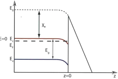
equal to the work function of the semiconductor, <5. . . . . 42
2-10 When the Fermi energy of the semiconductor is below the conduction
band edge, most emitted electrons come from states close in energy to
the edge of the conduction band. This presents a barrier height equal
2-11 For emission from the valence band, the majority of emitted electrons have energies close to the valence band edge. The barrier to transmis-sion is the sum of the semiconductor's electron affinity, Xe, and band gap energy, Eg. . . . . 48 2-12 For F = 5 x 10⁷V/cm, ND = 101 cm-3, and T = 300 K, the magnitude
of the band bending in silicon is approximately AO = 0.259eV. . . . . 50 2-13 Band bending near the surface of a semiconductor leads to the
for-mation of an accumulation layer and quasi-bound, discrete electronic states. In a MOS structure, the electrons in the accumulation layer can tunnel through the thin oxide layer from the substrate into the gate, leading to a current across the oxide layer. Figure adapted from [2]. . 52
2-14 Illustration of a nanowall emitter and the relative sizes of its dimen-sions. The structure is absolutely small in the x direction and has a quantum well width Lx in that dimension. The electric field Fm is applied from the z direction. . . . . 54
2-15 Normal energy diagram for a nanowall emitter. The presence of
trans-verse quantum confinement decreases the ERL in each subband and increases the reference zero-field barrier height relative to a bulk emitter. 56
2-16 A thin slab is absolutely small in the direction of emission, z, but
semi-infinite in the x and y directions. L, is small enough to consider the emitter to be quantum confined, discretizing energies in the emission direction . . . . . 57
3-1 Normally-unconfined emission (left) is characterized by a lack of quan-tum confinement in the direction of emission, while normally-confined emission (right) consists of an emitter confined in the emission direction. 63
3-2 Diagram of the infinite square well of width L and the first four energy
3-3 Diagram of the infinite cylindrical well of radius a . . . . 65
3-4 Normal energy diagrams for (a) bulk emitter, (b) normally-unconfined emitter that is also transversally confined, and (c) normally-confined emitter that is not transversally confined (c). . . . . 75
3-5 Emission from a bulk emitter (left) and normally-unconfined nanowall em itter (right). . . . . 78
3-6 Emission from a normally-unconfined rectangular nanowire (left) and normally-unconfined cylindrical nanowire emitter (right). . . . . 79
3-7 Emission from a normally-confined nanowall emitter. . . . . 82
3-8 Emission from a normally-confined nanowire emitter. . . . . 83
4-1 Electron constant energy surfaces of silicon. . . . . 87
4-2 Heavy hole and light hole constant energy surfaces for the valence band of silicon. The split-off band is excluded due to its maximum lying lower in energy than the heavy hole and light hole bands. ... 87
4-3 When projected into the k.-k. plane, the ellipsoidal constant energy surfaces of silicon become circles (characterized by mt) along the axis of emission and ellipses (characterized by mt and mi) on axes perpen-dicular to the axis of emission. . . . . 89
4-4 Plotting the ECD from an elliptical constant energy projection of a bulk emitter together with the ECD from the approximated circular constant energy projection with Em = E mtmi/mo shows that the approximation is in good agreement with the exact result. . . . . 90
4-5 The 3D constant energy surfaces of silicon are reduced to constant energy contours in 2D and constant energy points in ID. . . . . 91
4-6 For a 3D electron gas, AW is defined between two constant energy
surfaces and takes on continuous values, while for a 2D electron gas it
is defined between two constant energy contours of the same subband
index and is continuous within each subband. In the case of a ID
electron gas, AW is defined between two constant energy points in the
transverse plane and is entirely discrete. . . . . 92
4-7 The numerically-calculated total ECD with band structure effects (points)
and analytical, band-structure-corrected total ECD calculated via the
quasi-continuum approximation for a single circular constant energy
projection (solid) for a 1 nm NU nanowall as a function of the applied
field . . . . 9 3
5-1 ECD from the NU nanowall emitter, NU rectangular nanowire emitter,
and NU cylindrical nanowire emitter as a function of L2, L, = LY, and
2a respectively, with
#
= 5 eV and EF = 10 eV at F = 2 x 10⁷ V/cm. 1115-2 Normalized ECD of the NU cylindrical nanowire emitter and bulk
emit-ter with ya defined by the floating sphere model, with a constant
ap-plied field far from the emitter surface of FM = 1.145 x 10⁵ V/cm,
#
= 5 eV, EF = 10 eV, and an emitter height of I = 1 pm. The peakin the ECD curve occurs at a = dpeak, right of which field enhancement
dominates the ECD and left of which quantum confinement dominates
the E C D . . . . . 113 5-3 ECD from the NC nanowall and NC rectangular nanowire as a function
of L, and L. = L, respectively, with
#
= 5 eV and EF = 10 eV atF = 2 x 10⁷ V/cm. Plot points represent the average ECD per well
width, calculated from a Gaussian distribution of well widths with a
5-4 ECD from the first subband of an NC nanowall emitter with selected quantum well widths labeled (top left), quantum wells with widths equal to the labels in the ECD plot and the corresponding normal energy level in each well (top right), and the average number of emitted electrons from the subband as a function of the normal energy WQ (bottom ). . . . . 116 5-5 Correction factors for a bulk emitter, 1 nm NU nanowall emitter, and
1 nm x 1 nm rectangular nanowire emitter as a function of the applied field for the first subband, at T = 300 K, with
#
= 5 eV and EF= 5 eV. 120 5-6 Correction factors for the 15th (top), 10th, 5th, and 1st (bottom)sub-bands of a 10 nm NC nanowall emitter as a function of the applied field. The solid curves are the correction factors for the circular constant en-ergy cross sections, while the dashed curves represent the elliptical constant energy cross sections. . . . . 121
5-7 Correction factors for the 15th (top), 10th, 5th, and 1st (bottom) sub-bands of a 10 nm x 10 nm NC rectangular nanowire emitter as a func-tion of the applied field. The solid curves are the correcfunc-tion factors for the circular constant energy cross sections, while the dashed curves represent the elliptical constant energy cross sections. . . . . 121
5-8 The correction factors for NU emitters with EF < 0 are the same
be-tween emitter geometries. For low applied fields, the correction factors increase sharply, but converge to the ratio of the effective mass to the free electron mass for high applied fields. . . . . 122
5-9 FN plots for for an elementary bulk emitter, 5 nm NU nanowall emitter, 1 nm NU nanowall emitter, 5 nm x 5 nm NU rectangular nanowire
emitter, and 1 nm x 1 nm rectangular nanowire emitter for which EF = 10 eV,
#
= 5 eV. . . . . 1245-10 Experimental field emission data from a vertically-oriented single-layer
graphene sheet for three different voltage sweeps, overlaid by the ECD
predicted by Equation 5.17 for emitters with heights of 8.5 pm, 10.5
pm, and 14 jim. Dashed curves represent the ECD predicted for a
bulk emitter of equivalent geometry. . . . . 130
5-11 Field emission data from four sets of experimental setups, where a is
the SWNT radius,
I
is the SWNT length, and d is the SWNT-anode spacing: (a) a = 5 nm, I = 0.66 jim, d = 2 pm, (b) a = 7 nm,1
= 1.32pm, d = 2 pm, (c) a = 7 nm,
1
= 2.35 pm, d = 3.75 pm, and (d)a = 5 nm, I = 4.56 pm, d = 5.8 jim. Both the NU cylindrical nanowire equation and bulk emitter equation are plotted for each data set. . 131
C-1 The "semicylinder on emitter plane" model consists of a semicylinder
of radius p on a plane. The semicylinder and emitter plane form an
equipotential system . . . . 162
C-2 In the "floating cylinder at emitter plane potential" model, the center
of a cylinder of radius p is a distance 1 above the emitter plane. The
wire between the cylinder and the emitter plane indicates that they
form an equipotential system. . . . . 164
D-1 The accumulation well is bounded by the energy of the conduction
band edge in the bulk, the conduction band edge near the interface, and the semiconductor-vacuum boundary. . . . . 168
E-1 Normal energy diagram for emission from the NU nanowall. Lowering
#
reduces the barrier thickness seen at the reference energy WR and increases the transmission probability of electrons in that subband. . 177E-2 The ECD of the NU nanowall normalized to the FN equation, as a
function of the transverse well width L, with the work function as a parameter, for which F = 2 x 10⁷ V/cm, EF = 10 eV. . . . . 177
E-3 Normal energy diagram for emission from the NU nanowall. Decreasing
the effective mass of electrons in the well, m* causes all well energy lev-els to migrate upwards in energy, leading to a decrease in the reference state energy from WR to W and a reduced transmission probability for electrons in that subband. . . . . 178
E-4 The ECD of the NU nanowall normalized to the FN equation, as a function of the transverse well width L, with the effective mass m* as
a parameter, for which F = 2 x 10⁷ V/cm, EF= 10 eV,
#
= 5 eV. . . 178 E-5 Normal energy diagram for emission from the NU nanowall. Increasingthe applied electric field directly reduces the barrier thickness seen by electrons at reference energy WR, increasing their transmission proba-b ility . . . . 179 E-6 The ECD of the NU nanowall normalized to the FN equation, as a
function of the transverse well width L, with the applied field as a parameter, for which EF= 10 eV and
#
= 5 eV. . . . . 179 E-7 The normalized ECD of the elementary NU nanowall for selectedval-ues of EF. Above EF,Crit, changes in the Fermi energy do not affect the normalized ECD, while the ECD curve becomes discontinuous for Fermi energies below EF,crit . .. . .. . . . .. . . .. . . . . .. 182
E-8 The normalized ECD of the elementary NC nanowall for selected values
of EF. As EF decreases, the normalized ECD oscillations decrease in amplitude, become broader, and converge more quickly to the FN limit. For values of EF <- 0.2 eV, the ECD is normalized to a
List of Tables
2.1 Values for v and t as functions of y [3]. . . . . 31
4.1 Selected material parameters of silicon [4,5]. . . . . 88
5.1 Work functions extracted from FN plots and FN-type plots for which
EF= 10eV, q=5eV, and ya = 1. . . . . 125
D. 1 Normalized energy levels for the logarithmic well calculated via the
approximate JWKB method and exact three-point shooting Numerov
m ethod . . . . 171 D.2 The first five energy levels in the accumulation layer well as a function
of the donor dopant density in eV at T = 300 K. The conduction band
edge in the bulk is taken as the energy reference . . . . . 171
D.3 Emitted current density from the accumulation layer well of a bulk
sil-icon emitter (Jacc,bulk) and from the bulk silicon ECD equation without
band bending (Jbulk) for F = 2 x 10⁷ V/cm. . . . . 173 E. 1 The midpoint of the transition region between the NU nanowall and
bulk emitter, as determined by matching the extracted work functions
from the FN plot and NUFN plots for the nanowall emitter, given in
Chapter 1
Introduction
The terahertz (THz) regime, which lies between 0.1THz and 1OTHz, is one of the most promising, yet technologically underdeveloped, regions of the electromagnetic spectrum. Recently, this frequency range has garnered increased attention within the scientific community due to its wide variety of practical applications in astronomy [6], medicine and biology [7], chemistry [8], atmospheric science [9], security [10], [11], and defense [12]. However, taking advantage of the properties of THz radiation has been especially challenging due to the lack of radiation sources that can operate with a significant power output (above 1 W) in this frequency range. This has come to be known as the THz technology gap. Figure 1-1 plots the power output of state-of-the-art continuous-wave electromagnetic radiation sources against their operating frequency. Solid-state devices such as frequency multipliers, amplifiers, resonant tun-neling diodes, Impatts oscillators, and Gunn oscillators have achieved maximum op-erating frequencies of over 150 GHz, but are limited by the effects of electron velocity saturation, series resistance, and shunt capacitance as device sizes scale down [13]. Continuous-wave quantum cascade lasers (QCL) have demonstrated operation at fre-quencies as low as 0.84 THz, but must be cryogenically cooled to enable lasing at such low frequencies [14]. From the limitations of each of these types of devices, it
is clear that a new approach is needed. Vacuum nanoelectronic (VNE) devices are a Solid-State THz Sources (CW) 10000 1000 -100 10 100 10 0. 1 0---0 0 0.01 0.001 10 100 1,000 10,000 100,000 Frequency (GHz)
Figure 1-1: A plot of the output power vs. operating frequency of state-of-the-art continuous-wave terahertz sources shows a lack of devices with power outputs of 1 W or greater between approximately 100 GHz and 10 THz. QCLs are represented
by (0), frequency multipliers by (e) and other electronic devices by (-). Cryogenic results are plotted as hollow symbols.
prime candidate for bridging the THz gap. Unlike solid-state electronic devices, the electrons in VNE devices travel through vacuum and can have saturation velocities that approach the speed of light. As an advantage over QCLs, VNE devices natively operate at room temperature [15]. In addition, if the electron transit distance in a
VNE device is smaller than the mean free path of an electron in air, the devices need
not be operated in a vacuum at all. To date, multiple terahertz VNE devices, such as the integrated microcavity klystron [16], vacuum channel transistor [17], and micro Barkhausen-Kurz THz oscillator [13], have been proposed.
The primary active component of any VNE device is the electron source. These sources are typically implemented via an electron field emitter array (FEA), which consists of a large number of closely-spaced field electron emitters. Due to the require-ment of high current outputs from the electron source under low applied voltages [18] for VNE devices, it is desirable to reduce the lateral dimensions of field emitters for
larger electric field enhancement at the emitter tip and lower turn-on voltages. While
experimentalists have succeeded in fabricating FEAs based on nanoscale field emitters
in a variety of shapes and materials, such as carbon nanotubes [19], semiconductor
nanostructures [20], and graphene [21], theoretical treatments and modeling of new
types of field emitters have not kept pace. Primarily, as emitter dimensions shrink
into the nanoscale, the effects of quantum confinement and electric field
enhance-ment at the emitter tip play a significant role in determining the emitted current
density (ECD). Consequently, the oft-cited Fowler-Nordheim (FN) equation, which
was developed for and primarily applies to field emission from the planar surface of
a bulk metal may not be valid for predicting the ECD from nanoscale emitters. This
limitation of the FN equation is consistently overlooked in experimental studies and
FN-type equations are routinely used to describe the ECD from carbon nanotubes, semiconductor nanowires, and graphene sheets. While many studies have focused on
the electrostatics of nanoscale tip geometries [22-39], few have addressed the effects
of quantum confinement on the electron supply in the emitter.
This work develops a unifying framework for treating field emission that
incorpo-rates effects of quantum-confinement on the electron supply. The framework unifies
the existing ECD equations based on elementary models, such as the FN equation [40]
and nanowall equation [41], and generates ECD equations for quantum-confined
emit-ters of arbitrary geometry. In addition, the framework allows for an analysis of the
effects of quantum confinement on emitters, such as the dependence of the ECD on
the dimensions of the emitter. The ECD equations also provide an additional tool for
experimentalists to use when analyzing field emission data from nanoscale emitters.
This thesis is divided into six chapters. Chapter 2 reviews previous theoretical
and modeling work of field emission from metals, semiconductors, and
quantum-confined structures. A framework for treating cold field emission from metal emitters
specific emitter geometries are derived in Chapter 3. Chapter 4 extends the applica-bility of the framework to silicon field emitters by incorporating correction factors into the ECD equations that account for physical phenomena that were omitted in devel-oping the framework for metals. In Chapter 5, an analysis of the effects of quantum-confinement of the electron supply on the emitted current density from emitters of reduced dimensionality is performed, alternate data analysis procedures are proposed for quantum-confined emitters, and the ECD predicted by the model is compared to experimental field emission data from the literature for vertical graphene sheets and carbon nanotubes. Finally, a summary of the thesis, conclusions, limitations of the model, and proposed future work are covered in Chapter 6.
Chapter 2
Background
2.1
Fowler-Nordheim Equation
The first treatment of field electron emission came in 1928, with the publication of Fowler and Nordheim's "Electron emission in intense electric fields" [40]. This work produced the Fowler-Nordheim equation, which predicts the magnitude of the ECD emitted from the surface of a bulk metal: a metal large enough that the distribution of energy levels is assumed to be continuous. Fowler and Nordheim's model consisted of a Sommerfeld-type metal [42] at T = OK with an electric field applied normal to a planar surface of the metal. The metal is composed of an ideal gas of free electrons which obey Fermi-Dirac statistics and have mass m, the mass of an electron in free space. All electronic states up to a maximum energy EF, the Fermi energy, are
occupied by electrons. Electron momenta in each translational degree of freedom are assumed to be independent of each other and can be separated into components that are normal and parallel to the emitting surface. Electrons with momentum normal to the emitting surface are defined as normal electrons with normal energy W, while all other electrons are termed transverse electrons, with transverse energy Et, such that E = W
+
Et. The surface of the metal is taken to be planar, perfectly smooth, freeof defects, and to have a uniform local work function equal to <. The applied electric
field, F, does not penetrate into the metal and creates a nearly triangular potential
barrier between the metal and vacuum at the metal surface.
The emitted current density from a bulk metal, J (F) is proportional to the
prod-uct of the supply function, N (W), and transmission function D (F, W), as illustrated
in Figure 2-1. The total emitted current density is calculated by integrating over all
Electric Field
M e1ectrons per unit area, per unit time
Electrons D probability of electron
tunneling into vacuum
Figure 2-1: Field emission consists of electrons being emitted from a material that has an electric field applied to one of its surfaces. The magnitude of the emitted current density depends on the electron flux at the surface of the emitter and the probability of electrons tunneling from the material into vacuum.
normal energies and multiplying by the elementary charge, e:
J(F)=e IN(W)D(FW)dW (2.1)
In the FN model, the supply function quantifies the number of electrons passing
through a plane parallel to the emitting surface per unit area, per unit time. It is
calculated by integrating the product of the electron group velocity, density of states
in the direction of emission, density of states transverse to the direction of emission, and Fermi function over all k vectors in the transverse plane. The resulting supply
function is
4lrmokBT W[W-F1
N (W) =
ln
I+ exp[- k
J
(2.2)where kB is Boltzmann's constant, h is Planck's constant, T is the thermodynamic
temperature of the metal, W is the energy normal to the emitting surface, and EF
is the Fermi energy. The probability of an electron tunneling through the poten-tial barrier is determined by the transmission function, which is calculated using a Jeffreys-Wentzel-Kramers-Brillouin (JWKB)-type approximation [43-46]:
D (F, W)
~
exp [-goj
H -eV
(F, z)dz (2.3)_
1
where z is the emission direction, go = 47r/2mo/h, H = + EF - W is the height
of the potential barrier in the absence of an applied electric field (zero-field barrier height), V is the barrier potential, and 0 and Z are the classical turning points of the electron. For the exact triangular barrier V (F, z) = Fz and
D
(F, W)=
exp[
H3/2
(2.4)IF I
where B = (87r/3eh) V2mo is the second FN constant, and F is the electric field at
the surface of the metal. Figure 2-2 shows the relation between the electron normal energy, barrier height, and barrier thickness. Since most of the emitted electrons come from states near in energy to the Fermi energy, Equation 2.4 can be expanded about W
=
EF:D
(F, W) = exp [ #03/2 + c (W -EF) (2.5)FI
where c = 3B/45/2F is the transmission function decay rate [47]. Integrating the product of Equation 2.2 and Equation 2.5 over all energies normal to the emitting surface and multiplying by the elementary charge yields the total current density emitted from the metal. In order to obtain an approximate, analytical solution, the limit as T - 0 K is taken in Equation 2.2 and the lower limit of integration is extended from W = 0 to W = -oo. The result is the elementary Fowler-Nordheim equation,
Normal' Energy W-
---H=O+E
F-W W=EF F \ Wo-eFz-Figure 2-2: Normal energy diagram for a bulk metal emitter. As W increases, the barrier height seen by tunneling electrons decreases.
which predicts the magnitude of the ECD from the planar surface of a metal:
jh"em (F) = A#-'F 2e
xp
[ 3/2 (2.6)
where A = e3/87rh is known as the first FN constant.
Although the FN equation was derived from a basic physical model, it captures
the qualitative characteristics of cold field emission, such as the emitted current
den-sity's quadratic dependence on the applied field in the pre-exponential factor and its
-1/F dependence in the exponent. In experimental studies of field emission,
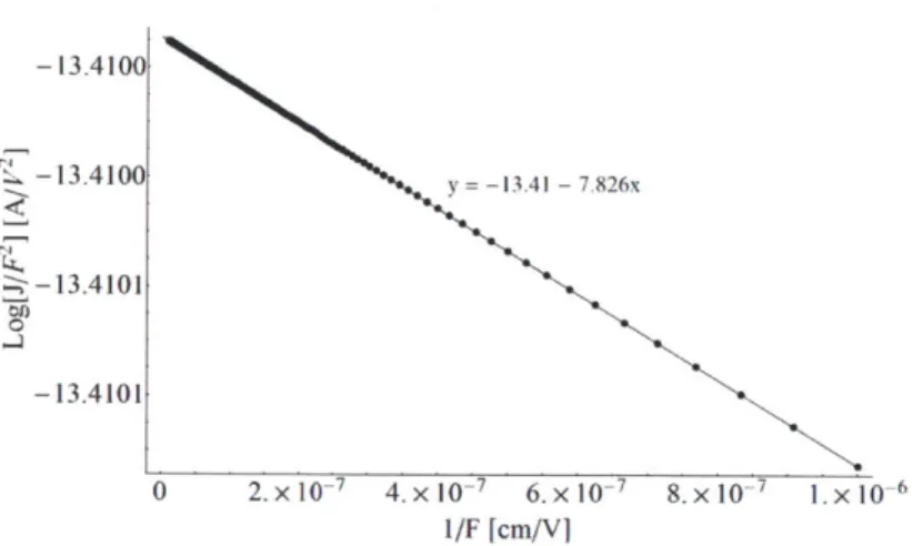
Fowler-Nordheim plots of ln [I/V 2]
vs. 1/V are constructed using the measured I-V data. If
it is assumed that I is linearly proportional to J and V is linearly proportional to F, an FN plot of field emission data should form a straight line. Aside from verifying
that an electron emission process is due to field emission, FN plots can be used to
extract the local work function (or field factor) by measuring the slope of a linear fit
to the data: m = -B# 3/2 . Figure 2-3 shows an FN plot and the extracted local work
function, 0.
The standard form of the FN equation does not use the exact triangular potential
- 13.4100 -13.4100 - 13.4101 - 13.4101 0 2. x 10~7 4. x 10~7 6. x 10-7 8. x 10-7 1. x 10-6 1/F [cm/VJ
Figure 2-3: Fowler-Nordheim plot for an emitter with
#
= 5 eV. The linear fity-intercept is equal to A and the slope is -B 3/2.
known as the Schottky-Nordheim barrier [48] and is shown in Figure 2-4. The barrier
Normal Energy
WR=E
W
HR=#
H=#+EF-W
Figure 2-4: Normal energy diagram for a bulk emitter with the Schottky-Nordheim barrier potential.
potential then takes the form
V(F,z) =
-167coz
Fz
(2.7)where co is the permittivity of free space. Substituting the potential from 2.7 into
y = -13.41 - 7.826x
Equation 2.3 yields a new form for the transmission function [49]
D (F, W) = exp F V [y] H3/2 . (2.8)
Expanding D about W = EF gives an approximate transmission function
D (F, W) ~ exp [ 3/2V [YEF] + c (W -
EF)
(2.9)
where [3,50] 3B C = 2Ft [yEF [ [y] = 1 + / - y2]1 E
(k2)
_y 2K
k2 v/2 1 /1 -y2~1 - y
2+
±y2ln[y]
2 2vy t [y] V [y] y (2.10) 3 dy.+
1 [y2 _ Y2In
[y]] 9 k2 2/1 -y 2 I+ V1 -y 2 Y /e3F/47rEo0 +
EF -W'YEF =/e 3F/47rco/#, K (k2) is the complete elliptic integral of the first kind, and E (k2
) is the complete elliptic integral of the second kind. In general, these values
must be calculated numerically, but good analytical approximations for v and t exist
via the work of Forbes, as listed above. The exact values for v and t as functions of
y are given in Table 2.1. Proceeding as in the case of deriving the elementary FN
y 0 0.10 0.20 0.30 0.40 0.50 0.60 0.70 0.80 0.90 1
u (y) 1.000 0.982 0.937 0.872 0.789 0.690 0.577 0.450 0.312 0.161 0
t (y) 1.000 1.004 1.011 1.021 1.032 1.044 1.057 1.070 1.083 1.097 1.111
Table 2.1: Values for v and t as functions of y [3].
equation [47]:
J Stan (F) = A- 1t [YEF -2 F 2 e [YEF] 032 (2.11)
As can be seen by looking at the values taken by v and t, the incorporation of the
image potential increases the transmission probability and emitted current density
for a given applied field relative to the exact triangular barrier.
2.2
Fowler-Nordheim-Type Equations
While Fowler and Nordheim's results formed the foundation of the theory of field
emission, their model was not complete. Due to non-ideal effects, the FN equation
predicts ECDs that are significantly lower than experiments have shown for metal and
semiconductor emitters [51]. To improve the accuracy of models for field emission, multiple correction terms have been appended to the standard FN equation to account
for these non-idealities. This equation is known as the physically-complete
Fowler-Nordheim equation:
JP (F) = ATBAP AO AY2F 2
Pexp B /03/2 (2.12)
where AT is a temperature correction factor, AB is the band structure correction factor,
-ya is a field enhancement factor, Ap is a tunneling prefactor correction factor, AT is
a decay rate correction factor, P is the tunneling prefactor, and V is a barrier-shape
2.2.1
Temperature Correction Factor:
ATThe standard Fowler-Nordheim equation is a result of taking the limit as T -+ 0 K of the integrated product of the elementary charge, supply function, and transmission function. If this limit is not taken, the emitted current density is weakly dependent on temperature within the field emission regime. For a bulk emitter, the temperature correction factor to first order takes the form [47]
XT -
wrckBT
sin [7rckBT]
Accordingly, when the limit as T -+ 0 K is taken, AT evaluates to unity.
2.2.2
Band Structure Correction Factor:
AB
By using the free electron mass and assuming spherical constant energy surfaces
when deriving the Fowler-Nordheim equation, all band structure details specific to the emitter material are ignored. In actuality, the constant energy surfaces of a material are not spherical and are characterized by the shape of the conduction band minimum and valence band maximum. Many studies of varying levels of complexity and detail have investigated incorporating band structure effects into field emission calculations, ranging from directly calculating electron wave functions [52,53] to using the effective mass approximation [54]. For the purposes of this framework, an analytical method was desired and the approach of Stratton was chosen to address band structure effects. Stratton was the first to incorporate band structure effects into field emission calculations, as part of a study of field emission from semiconductors. In his work, he assumes the emitter material has a spherical constant energy surface characterized
by an isotropic effective mass m,. Later, this treatment of band structure effects
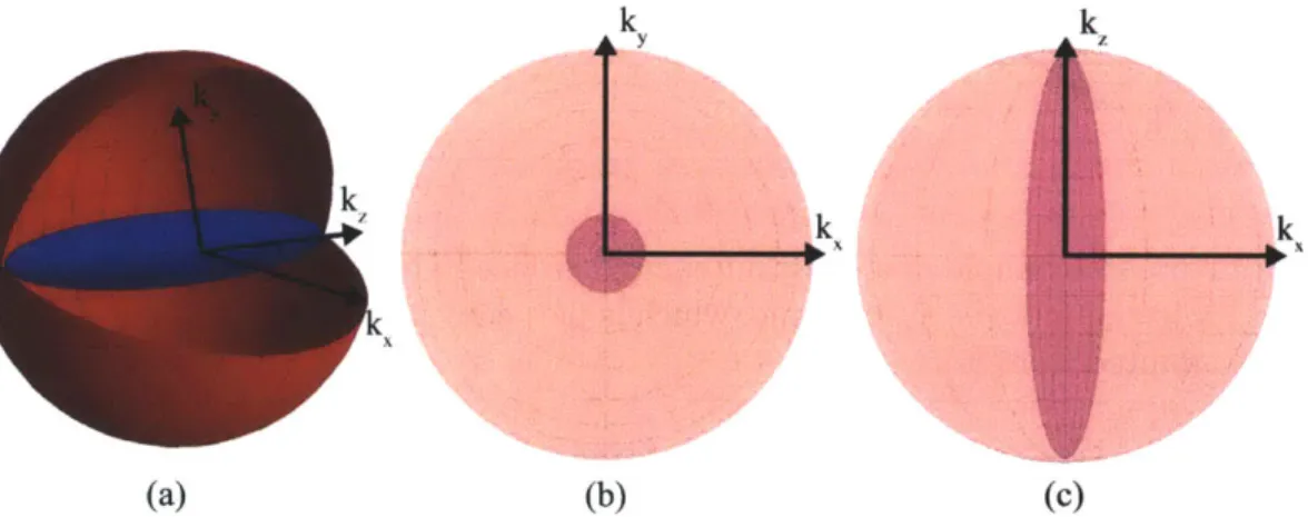
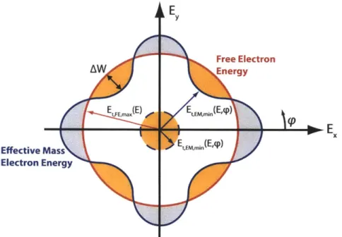
was generalized to include constant energy surfaces of arbitrary geometry, such as the one in Figure 2-5, by Gadzuk and Plummer [1]. Although comparatively simple, this
*kZ
Figure 2-5: An example of a constant energy surface. This constant energy surface is being projected into the k,-ky plane, which is perpendicular to the emission direction. Figure adapted from [1].
approach has been used to reconcile qualitative discrepancies between experimental
and theoretical total energy distributions from single emitters [55].
The energy of an electron is given by
h
2k
2h
2k2h
2k22m, 2my 2m, (2.14)
where mX, my, and mz are the effective masses in the x, y, and z directions. A constant energy surface is generated by all points in k-space at which the sum of the energy components is equal to E. For the free electron constant energy surface, mx = my =
'mz = MO, forming a spherical shell in k-space. However, electrons in semiconductors are often characterized by effective masses in the x, y, and z dimensions that are different from the free electron mass. Thus, for a given set of effective masses that
-- kbW
are not equal to m0 , the constant energy surface defined by the effective masses will
be larger or smaller than the free electron constant energy surface in some regions, as shown in Figure 2-6. Since the volume enclosed by each of the constant energy
surfaces represents the total number of electronic states contributing to the ECD, the
volume between constant energy surfaces represents the excess number of electronic
states that contribute to the free electron ECD, but should be omitted to calculate
the ECD solely from the semiconductor. The goal of these band structure corrections
is to calculate a correction ECD from states that lie between the free electron and
emitter material's actual constant energy surfaces, then subtract it from or add it to
the free electron ECD to obtain the ECD from the emitter.
k k
(a) (b) (c)
Figure 2-6: (a) Ellipsoidal constant energy surface with mo > m, > m, my (blue)
compared to the free electron constant energy surface (red), (b) ellipsoidal and free electron constant energy surfaces projected into the kX - ky plane, and (c) ellipsoidal
and free electron constant energy surfaces projected into the kX - k, plane.
Assuming that the momentum of the electrons is uncoupled between
transla-tional degrees of freedom, the electron energy can be split into normal energy W
(kz-direction) and transverse energy Et (kx-kv plane). This separation of energies
allows for the constant energy surfaces to be projected into the transverse plane and
the integral over all k space to be separated into a transverse part and a normal part.
maximum transverse k-vector and minimum transverse k-vector value that define the shape of the projected constant energy surface. The corrected ECD is calculated by integrating over all transverse k vectors and all free electron energies via the following equation [1]:
00
kt (E )J (F, T)= -
f
(E) dE D (E, kt) ktdkt +(2r)-l7r h J 1
X 27r kt(E,) ktin (E,#))
]
0c
kkt(E0) kfin(E,O)(2.15)
where e is the elementary charge and D (E, kt) is the transmission function. If con-sidered in terms of the transverse energy, the integration is performed between a min-imum effective mass (EM) transverse energy, Et,EM,min, and some maximum
trans-verse energy, Et,EM,max. For free electrons (FE), the minimum transverse energy is
Et,FE,min= 0 and the maximum transverse energy possible at an energy E occurs
when W = 0, leading to Et,FE,max = E. In the transverse plane, the states that
contribute to the free electron ECD are located between Et = 0 and Et = E, while states that contribute to the effective mass ECD are located between Et,EM,min and
Et,EM,max, which are functions of
#
in general, as shown in Figure 2-7. When the trueconstant energy surface of the material is smaller (larger) than the free electron con-stant energy surface, electron states have been erroneously counted towards (omitted from) the actual ECD and must be subtracted from (added to) the free electron ECD as a correction term. For each free electron energy E and angle 0, there will be a discrepancy between the maximum transverse free electron energy and the maximum transverse effective mass electron energy. Since this energy is the difference between a total energy and a transverse energy, it can be considered to be a normal energy
AW. When AW is positive, it is considered an energy surplus, while when AW is
AW EtE a(E) Effective Mass Electron Energy
EY
Free Electron Energy E (E,(p) E ,EM,min(E,(p)Figure 2-7: Actual and free electron constant energy surfaces projected into the
E.-Ey plane. The area inside the red (blue) contour represents electron states that contribute to the free electron (actual) ECD. Areas shaded gray (orange) are electron states that contribute to the actual (free electron) ECD, but are excluded by the free electron (actual) ECD. If the constant energy surface has a neck, it is projected as an absence of electronic states in the E,-E, plane and therefore is also shaded orange. Figure adapted from [1].
In order to proceed further in calculating the emitted current density, a specific
material must be designated and the shape of its constant energy surfaces must be
defined. Because the result of this particular calculation is used extensively in this
thesis, the constant energy surfaces will be taken as spherical shells characterized
by an isotropic effective mass rnm. Changing coordinates from kt to Et and taking
into account that spherical constant energy surfaces are independent of #, the ECD equation becomes
J(F,T)
4=r
n
0 0 dE EmV3 o JO
dE D (E - Et)
I1+exp[(E - EF) kBT]
where Em = (m,/mo) E is the maximum value of Et,EM for a given value of E and EF is the Fermi level. Making another variable change with W = E - Et and integrating (2.16)
over Et gives an equation of the form
J(F, T) =
e 7
BTJ
dWln1 +
exp [EF-W1(2.17)
x{D(W)- [-E (W)]
D(W-Em(W))
where E (W) is the derivative of Em (W) with respect to W. The details of the
variable substitution and integral transform are given in Appendix I of [54]. Inserting the expression for Em above and defining y, = 1 - (mn/mo) gives the equation for ECD with band structure corrections:
4mokBT
*~F-J
(F, T)= e
47 BT dW In1
+ exp[{D
(W) - D ('yW)}h0
.
kBT __
( ) - y D( -n~ (2.18)After specifying a form for the transmission coefficients and a value for the effective mass, an ECD equation can be derived. Factoring out all terms common to the Fowler-Nordheim equation gives a term of the form AB = 1 - C, where C includes
the band structure effects.
2.2.3
Field Enhancement Factor: a
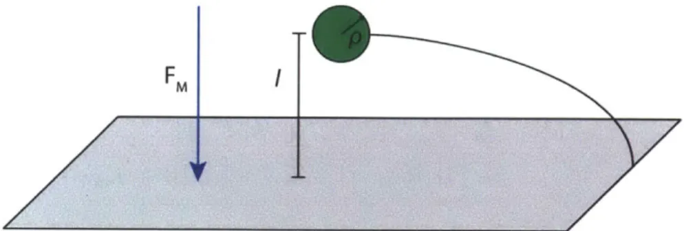
Basic electrostatics dictates that the electric field at the surface of a cathode depends on its geometry. Rounded or pointed surfaces, such as the tips of field emitters, cause the electric field to be amplified at the apex relative to the surrounding applied field. Many models have been proposed for the field enhancement at the tip of a field emitter such as the ball-in-a-sphere model [27], hemisphere on a plane model [56], floating sphere between two plates model [31, 32], hemisphere on a post model [33, 38, 57], and hemi-ellipsoid on a plane model [31]. While the hemisphere on a post model is the most physically realistic for emission from thin whiskers, it comes at the cost of requiring numerical methods to evaluate the electric field at the emitter tip.
FM
hFigure 2-8: A schematic for the "floating sphere at emitter plane potential" model. The center of the sphere of radius p is located a distance
1
above the emitter plane. Far away from the sphere, the electric field is FM, while at the apex of the sphere it is approximately (3.5 +l/p)
Fm.For emitters with large aspect ratios (emitter height to emitter width), the floating sphere at emitter plane potential model, shown in Figure 2-8, serves as a good semi-analytical approximation. In this model, the emitter tip is taken as a sphere that is floating in space above an emitter plane. The sphere is held at a uniform potential equal to that of the emitter plane below it. The field enhancement factor at the apex of the sphere is found to be [31]
a = 3.5 + - (2.19)
p
where I is the height of the center of the sphere above the emitter plane and p is the radius of curvature at the emitter tip.
2.2.4
Tunneling Prefactor and Correction Factor: P and Ap
The form of the JWKB approximation appropriate for deriving the transmission func-tion is dependent upon the shape of the potential barrier. The most mathematically rigorous and exact of these forms was derived by Fr6man and Fr6man (FF) in the 1960s [58]:F
exp [-G]
D (P, G) =+Pexp [-G]
(2.20)
where P is the tunneling prefactor and G is the JWKB exponent given by
G = goJ M (z)1/2 dz (2.21)
with go = 47r (2mo) /h, M = U (z) - W, and U (z) being the specific form of the
1D barrier potential. The integration is performed over all positive values of M,
between the classical turning points of the electron. This expression for the
trans-mission function is general and all other forms of transtrans-mission functions from JWKB
approximations can be obtained from it by employing the proper approximations [59].
The validity of the approximations made to the FF JWKB expression is qualified
by the shape of the potential barrier. Barrier shapes are classified as either weak
(e-G ~ 1) or strong (e-G < 1) and ideal (P = 1) or non-ideal (P z 1) [59]. The form
of the JWKB expression used in deriving the standard FN equation [47] corresponds
to that of a strong, ideal barrier potential and is given by the "simple JWKB" form
D (G) = exp [-G] . (2.22)
However, according to Forbes [59], the exact triangular barrier (along with others) is
not an ideal barrier potential and P # 1. In the limit of the strong barrier regime, the proper form of the transmission function should be that proposed by Landau and
Lifschitz (LL) [60]. The LL formula is the simple JWKB expression with the addition of a tunneling prefactor
D (P, G) = P exp [-G] . (2.23)
In general, the tunneling prefactor depends on the normal energy and after
integra-tion over all normal energies produces a correcintegra-tion factor Ap that is dependent upon
the form of P. For barriers with exact, analytical solutions for the electron
and making approximations (usually strong barrier) to arrive at an expression with
the form of the LL formula. This procedure has been carried out for the rectangular
barrier, exact triangular barrier, parabolic barrier, and Eckert barrier [59]. For
po-tential barrier shapes without analytical transmission probability solutions, P must
be determined numerically.
2.2.5
Barrier Shape and Decay Width Correction Factors: v
and
AT
If nearly-triangular potential barrier shapes are used instead of the exact triangular
barrier, they can be incorporated into FN theory by way of a barrier shape correction
factor, v. One of the most common potential barrier shapes used is the
Schottky-Nordheim barrier [48] shown in Figure 2-4 and given by Equation 2.7. Using this
potential barrier, the barrier shape correction factor takes the form v [y] as derived
in the standard Fowler-Nordheim equation above [49]. When a transmission function
incorporating v is expanded about a particular normal energy, it generates an
addi-tional correction term that is grouped with decay rate, c. After the final integration
step over all normal energies in deriving the ECD equation, this additional term, called the decay rate correction factor, appears in the pre-exponential factor and is
denoted by A,. In the standard FN equation, A, = t-2
[
e3F/4rco/1].2.3
Emission from Semiconductors
When treating field emission from metals, electrons are emitted from the conduction
band and the majority of them have energies close to the Fermi level, which is positive
with respect to the conduction band edge. In the case of semiconductor emitters, the
Fermi level may be negative with respect to the conduction band edge and emission