HAL Id: hal-02351754
https://hal.archives-ouvertes.fr/hal-02351754
Submitted on 27 Nov 2020HAL is a multi-disciplinary open access archive for the deposit and dissemination of sci-entific research documents, whether they are pub-lished or not. The documents may come from teaching and research institutions in France or abroad, or from public or private research centers.
L’archive ouverte pluridisciplinaire HAL, est destinée au dépôt et à la diffusion de documents scientifiques de niveau recherche, publiés ou non, émanant des établissements d’enseignement et de recherche français ou étrangers, des laboratoires publics ou privés.
A fabrication process for self-connected horizontal SiGe
nanowires
M. Merhej, S. Ecoffey, B. Sadani, B. Lee–sang, Thierry Baron, S. David, D.
Drouin, B. Salem
To cite this version:
M. Merhej, S. Ecoffey, B. Sadani, B. Lee–sang, Thierry Baron, et al.. A fabrication process for self-connected horizontal SiGe nanowires. Microelectronic Engineering, Elsevier, 2019, 220, pp.111150. �10.1016/j.mee.2019.111150�. �hal-02351754�
1
A fabrication process for self-connected horizontal SiGe
nanowires
M. Merhej a, b,c, S. Ecoffey b,c, B. Sadani b,c, B. Lee – Sang b,c, T. Baron a, S. David a,
D. Drouin b,c *, and B. Salem a *.
a- Univ Grenoble Alpes, CNRS, LTM, F-38000 Grenoble, France
b-Laboratoire Nanotechnologies Nanosystèmes (LN2) - CNRS UMI-3463, Université de Sherbrooke, 3000 Boul. Université, Sherbrooke, J1K 0A5, Qc, Canada.
c-Institut Interdisciplinaire d'Innovation Technologique (3IT), Université de Sherbrooke, 3000 Boul. Université, Sherbrooke, J1K 0A5, Qc, Canada.
*to whom correspondence should be addressed: [email protected] and [email protected]
Keywords: Vapor–liquid–solid (VLS) growth, Silicon germanium nanowire (SiGe NW), Horizontal growth, Nanotrenches,
Abstract
We present in this paper a low thermal budget process for self-connecting horizontal silicon-germanium nanowires. The guided nanowires on amorphous oxide layer have been elaborated by a chemical vapor deposition (CVD), using vapor-liquid-solid (VLS) mechanism, via a gold catalyst. We have optimized the growth parameters on reference samples with pre-patterned electrodes on SiO2/Si substrate. To
control and eliminate the random growth of horizontal NWs, we have developed a technological process to guide these nanowires in nanotrenches created in the oxide to locate gold catalysts and confine planar growth. The silicon germanium nanowire (SiGe NW) connected the predefined electrodes showed an electrical behavior of an intrinsic SiGe NW.
I.
Introduction
Three-dimensional (3D) integration is a promising complementary approach of the conventional planar technologies. It allowsleveraging interconnect delay latency, increases overall performance and energy efficiency and decreases the footprint of an Integrated Circuit (IC) [1]. Today, 3D ICs in which active devices are vertically stacked upon each other, have shown significant power gains for different applications like memory-on-logic [2]. This 3D technology relies on vertical interconnects between circuit layers known as Through Silicon Vias (TSVs). Different strategies are adopted in the 3D-ICs integration: chip level [3] and wafer level [4]. The monolithic 3D integration [5][6] is another lower-cost 3D approach, that offers the possibility to elaborate new circuit layerssequentially over the previously fabricated layers,
2
and on the same substrate. A major processing difficulty of this attractive technological approach is that the fabrication process in the upper layers circuitry must be below 550 °C [6] in order to preserve the performances of the devices in the front-end of the line (FEOL). Recently, self-assembled horizontal semiconductor nanowires, prepared by bottom-up techniques has spurred a new interest in the fabrication of nano-devices. This bottom-up technique provides cost-effective nanowires compared to the top-down technique [7], with respect to the thermal budget for 3D integration processes. It allows for an extremely reduced nanowires dimension and a wide choice of materials and compositionsfor integration with planar devices.
Currently, there are mainly two general strategies to address the challenging alignment and to fabricate self-assembled horizontal NW based FETs: an indirect post-growth assembly or a direct assembly. Post-growth assembly in liquid, such as dielectrophoresis is an indirect approach that was used in orderto create arrays out of randomly dispersed nanowires [8]. This strategy requires specific fabrication processes to create a contact pad and metal wires, for applying non-uniform AC signals. Connecting NWs with a precise alignment over a large area is considered as the main obstacle for post-growth assembly. Recent studies have shown a well ordered and precise NWs directly assembled during their CVD-VLS growth [9][10]. Device fabrication using planar NW growth without any crystalline seed is still facing difficulties [11], therefore direct growth between pre-defined electrodes could be an effective alternative [12]. We propose in this work a low thermal budget process to electrically connect self-assembled horizontal silicon-germanium nanowires (SiGe NWs). We first present the horizontal growth parameter optimization at a low temperature between predefined electrodes, on a SiO2/Si
substrate. Afterward, we propose a technological process to control and eliminate the random growth of horizontal NWs. Finally, we present this guided growth according to different parameters including the wet etching, and the width of the trenches. We show the first electrical results of a connected nanowire between metal electrodes.
II.
Experiment and methodology:
A preliminary study on a SiO2/Si substrate with two predefined metallic electrodes has been
established to optimize the growth parameters of the horizontal SiGe NW. The NWs growth have been conducted into a Chemical Vapor Deposition (CVD) furnace, using patterned
3
electrodes of gold seed layer covered with 120 nm titanium which is used as a protected layer (see Figure 1). A 90 sccm of silane and 45 sccm of germane (~10% in H2) gas precursors were
used as a source of silicon and germanium respectively, 40 sccm of HCl as reactive gases [13], and H2 as a carrier gas.
Figure 1: Schematic illustration of a direct growth SiGe NW between two predefined deposited and patterned electrodes.
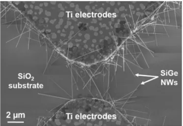
For temperature below 400°C, no growth has been detected, while SiGe NWs horizontal growth was observed over the range of 400-450°C. It was determined that a 40 min NW growth at 450°C with a pressure of 4.5 Torr produces a 2.5-4.5 µm nanowire length to connect the electrodes as shown in figure 2. This study also shows the importance of a well-guided growth to fabricate NW based FET since neither number nor connectivity control has been obtained. We note that the nanowires growth has taken place between the pre-defined electrodes, with nucleation on the pad trenches (gold layer).
Figure 2: SEM image of SiGe NWs grown by Vapor-Liquid-Solid mechanism between two pre-defined electrodes on an oxide plane surface.
4
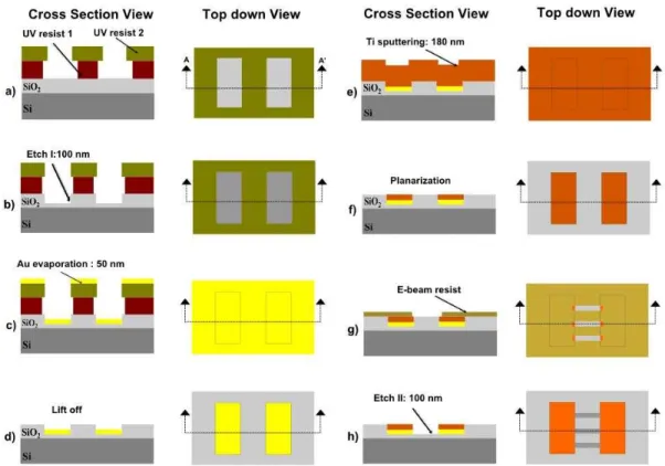
Based on the optimized growth parameters, a damascene process was developed on 150 nm thick silicon dioxide thermally grown on a silicon substrate. The damascene process with nanotrenches in which the NWs will be guided is detailed in Figure 3. This process combines photolithography, dry/wet etching, electron beam lithography, and chemical-mechanical planarization techniques. The damascene method proposed in this work benefited from the previous development related to the fabrication of single electron transistors [13], and top-down ultra-thin nanowires [14].
First dummies structures and contact electrodes are patterned in the dielectric using photolithography [step (a) of figure 3]. Then these structures are etchedusing an ICP reactive ion etching [15] to create 100 nm deep microtrenches [step b of figure 3]. The dummies are essential for planarization uniformity [16]. A Titanium film (5 nm) and gold film (50 nm) were deposited inside the trenches using e-beam evaporation [step c of figure 3], followed by a lift-off [step d of figure 3].
Another 150 nm titanium film deposited by sputtering over the entire sample, in a way to fill the trenches on the top of the gold catalyst [step e of figure 3]. This titanium layer has to be thicker than the deepest trenches of the sample, to enhance CMP quality, and ensure uniformity of the planarization [17]. The CMP is used to eliminate all excess titanium material above the original oxide surface, and to planarize trenchesdown to the SiO2 surface [step f of figure 3].
These CMP experiments have been carried out on 10×10 mm2 Si samples. A commercial slurry with 50 nm silica nanoparticles diluted in isopropyl alcohol (IPA) in 1:1 volume ratio was chosen. The selectivity studies on both materials have been used to control planarization at a nanometer scale [18]. Finally, 100 nm deep perpendicular nanotrenches were patterned using an e-beam lithography (EBL) on a ZEP resist [step g of figure 3], followed by an ICP plasma etching in the oxide layer [step h of figure 3]. The fabricated nanotrenches are 2 µm long, while the width varies from 70 nm to 1µm, depending on the EBL patterns.
Figure 4 depicts a SEM top view image of a 100 nm deep nanotrenches in the dielectric layer, after the final etching step at the end of the pre-described process. The darker lines represent 2 µm wide predefined titanium electrodes, while the brighter color reflects the oxide material.
5
Figure 3: The damascene process for guided horizontal nanowire growth. The left side of each part of the figure is the cross section along the AA’ axis. a) A UV lithography is realized to pattern the titanium electrodes over the oxide layer grown on a silicon substrate. b) 100 nm trenches are formed into the oxide layer. c) A 50nm gold film is deposited on the surface using e-beam evaporation and d) then removed from the surface by a lift-off technique. e) A 180nm titanium film is deposited by sputtering over the entire device area and f) then planarized with CMP down to the SiO2 surface with the Au/Ti metal stack is embedded in the oxide layer. g) E-beam lithography is used
to pattern different sizes of nanotrenches into the oxide. h) A second 100 nm oxide etching step is made to create nanotrenches between the electrodes.
Figure 4: SEM image of the oxide nanotrenches created between titanium electrodes. The bright color represents the oxide while the dark color depicts the titanium.
A morphological FIB-STEM characterization has been conducted on the nanotrenches. This observation revealed a remaining oxide layer on the sidewalls of the microstructures, as shown in figure 5. This oxide on the edge of the gold seed acts as a barrier and prevents any NW
6
growth. It is due to the combination of two factors: i) the plasma etching of the micro-trenches where the sidewalls are not vertical (90°) and ii) the plasma etching of the nano-trenches where the remaining Ti acts as a non-intended hard-mask that leads to a non-vertical etching.
Figure 5: FIB–STEM images revealing the remaining silicon oxide layer the Au catalyst at the end of the UV trench sidewalls after the final etching step of the nanotrenches.
To eliminate the remaining SiO2 layer on the nanotrenches sidewall, an extra wet etching step
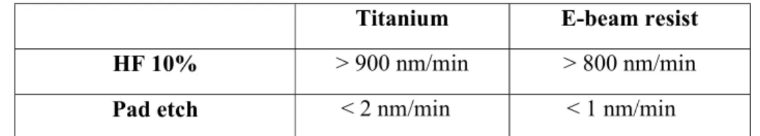
is added to the process before removing the resist. This etching must be isotropic and very selective in the thin films of both Ti and resist. For that different wet etching solutions have been evaluated: hydrofluoric acid HF (10%) based-solution a commercial solution known as “Pad-etch” [19]. Table 1 shows the etching rates of HF (10%) and “Pad-etch” solutions versus deposited titanium and e-beam resist films. While HF is the preferred solution to wet etch the SiO2 , its etch rate versus Ti and resist is too fast to allow a good control on thin films.
Titanium E-beam resist
HF 10% > 900 nm/min > 800 nm/min
Pad etch < 2 nm/min < 1 nm/min
Table 1: Etch rate comparison on titanium and e-beam resist films between HF (10 %) and Pad-etch based etchant solutions.
Figure 6 shows etched Ti and SiO2 thicknesses versus time for HF and Pad-etch solutions. The
Pad-etch [20] solution has similar etch rates as HF, however its selectivity versus Ti is far better. HF solution etches Ti almost as fast as SiO2 under certain conditions.
The surfactant used in the Pad-etch [20] allows to obtain low etch rates on titanium because it acts as a corrosion inhibitor. After a certain amount of time (between 30 and 40 s on Fig. 6),
7
the preferential adsorption of the corrosion inhibitor on the TiO2 is decreased due to the etching / removal of the TiO2 layer and thus appearance of the Ti surface. The Ti is then etched rapidly in the pad etch solution.
The “pad-etch” solution has been used on the samples after nanotrenches plasma etching process and before resist removal. A final acetone/IPA cleaning removes all the remaining resist film before loading the samples into the CVD machine.A 40 min VLS growth is carried out at 450° C with a pressure of 4.5 Torr immediately after the cleaning to avoid further oxidation.
Figure 6: Average oxide and titanium removal thickness as a function of the time, for different etchant solutions.
III. Results and Discussion
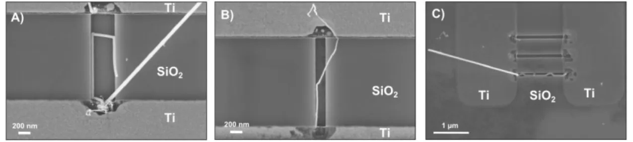
Figure 7 depicts nanowire growth in different nanotrenches cavities dimensions with the optimized fabrication process described above. The width of these cavities varies between 500 nm (figure 7-A), 200 nm (figure 7-B), and 100 nm (figure 7-C). The NW growth took place in different trenches regardless of their widths. Among 10 samples tested with 100 different nanotrenches each, the yield of the nanowires growing inside the cavities is about 5 to 10 %. This limited yield is attributed to a poor control of the pad-etch process. The presence of many empty trenches is probably due to the wet etching time used. Indeed, this time is not long enough to eliminate the entire oxide layer on most of the trenches. Nevertheless, and on other nanotrenches, this time was enough to remove the oxide and expose the catalyst. Figure 7-C is
8
an example that shows a non-homogeneity in growing NWs inside the trenches. This reflects the optimization needed to have a better control of the wet etching process mainly by controlling the etching and over etching time to completely remove the SiO2 on the sidewalls. Further
optimization of the nanowire nucleation is also needed.
Several nanowires could nucleate from a rectangular gold region. The trench width impacts the growth following the initial nucleation. The transport limitations influence local precursor pressures and thus induce kinking. The contact between the sidewall trenches and the liquid catalyst play an important role to maintain a straight nanowire inside the cavity, thus to connect the electrodes. Indeed, different physical effects such as surface chemistry and roughness, adhesion, temperature, and pressure can affect the frictional forces that exist between the sidewalls and the liquid catalyst [21]. If a guided assembly is to be achieved, efficient nucleation will also be required.
Our fabrication scheme allowed a preliminary demonstration for the elaboration of different single nanowires, where only one nanowire connected a pair of electrodes to fabricate S/D contacts. Optimization of the plasma and the wet etching processes is ongoing to increase the yield of NWs growth, and get a deeper understanding of the guided NW growth to control it.
Figure 7: Nanowire growth in several nanotrenches cavities dimensions a): 500 nm width, b): 200 nm width, c) 100 nm width.
The electrical properties of the final SiGe NW device (figure 8-a) are extracted as a function of source-drain biases using a semiconductor parameter analyzer (Keithley4200), at room temperature. I–V characteristics are measured for an individual intrinsic SiGe NW which is located between titanium electrodes, as shown in figure (8-b). The current-voltage curve reveals a typical Schottky behavior. However, the overall resistance differs according to the sign of the applied drain voltage, thus revealing an electrical dissymmetry of the source and drain contacts (Figure 8-c). This phenomenon can be referred to a non-uniform cover of the titanium electrode
9
that connects the nanowire. An additional silicidation process is considered as a solution to reduce the contact resistance between the nanowire and the metal, and thus enhance the electrical properties [22].
Figure 8: SEM micrographs of a) the contact pad area (in square) for electrical measurement and b) SEM image of a SiGe NW grown by VLS inside a nanotrenche (100 nm width) between two titanium/gold pre-defined electrodes. c) Output characteristics of the connected intrinsic SiGe NW with voltage varying from -1 to 1 V.
IV. Conclusion
In conclusion, a preliminary demonstration of planar SiGe NWs grown via a bottom-up (VLS) technique over a dielectric surface has been demonstrated. This process can be implemented in the back end of the line since all fabrication steps respect the thermal budget. It may offer a direct contact between the SiGe NWs and metallic source/drain electrodes without any additional treatments for aligning. Connected NWs between predefined electrodes can be exploited as channels to fabricate nanowire-based devices in the BEOL for further device development.
V.
References
[1] M.M. Shulaker, T.F. Wu, M.M. Sabry, H. Wei, H.P. Wong, S. Mitra, Monolithic 3D Integration : A Path From Concept To Reality. (2015) 1197–1202.
[2] D. Dutoit, C. Bernard, S. Cheramy, F. Clermidy, Y. Thonnart, P. Vivet, C. Freund, V. Guerin, S. Guilhot, S. Lecomte, G. Qualizza, J. Pruvost, Y. Dodo, N. Hotelier, J. Michailos, A 0.9 pJ/bit, 12.8 GByte/s Wide IO memory interface in a 3D-IC NoC-based MPSoC, VLSI Technology (VLSIT) Symposium on. (2013) 22–23.
[3] S.F. Al-sarawi, D. Abbott, P.D. Franzon, A review of 3-D packaging technology, IEEE Transactions on Components Packaging and Manufacturing Technology Part B. 21 (1998) 2–14.
[4] M. Koyanagi, H. Kurino, K.W. Lee, K. Sakuma, N. Miyakawa, H. Itani, Future system-on-silicon LSI chips, IEEE Micro. 18 (1998) 17–21.
10
[5] C.H. Shen, J.M. Shieh, T.T. Wu, W.H. Huang, C.C. Yang, C.J. Wan, C.D. Lin, H.H. Wang, B.Y. Chen, G.W. Huang, Y.C. Lien, S. Wong, C. Wang, Y.C. Lai, C.F. Chen, M.F. Chang, C. Hu, F.L. Yang, Monolithic 3D chip integrated with 500ns NVM, 3ps logic circuits and SRAM, Technical Digest - International Electron Devices Meeting, IEDM. (2013) 4–7.
[6] P. Batude, C. Fenouillet-Beranger, L. Pasini, V. Lu, F. Deprat, L. Brunet, B. Sklenard, F. Piegas-Luce, M. Casse, B. Mathieu, O. Billoint, G. Cibrario, O. Turkyilmaz, H. Sarhan, S. Thuries, L. Hutin, S. Sollier, J. Widiez, L. Hortemel, C. Tabone, M.P. Samson, B. Previtali, N. Rambal, F. Ponthenier, J. Mazurier, R. Beneyton, M. Bidaud, E. Josse, E. Petitprez, O. Rozeau, M. Rivoire, C. Euvard-Colnat, A. Seignard, F. Fournel, L. Benaissa, P. Coudrain, P. Leduc, J.M. Hartmann, P. Besson, S. Kerdiles, C. Bout, F. Nemouchi, A. Royer, C. Agraffeil, G. Ghibaudo, T. Signamarcheix, M. Haond, F. Clermidy, O. Faynot, M. Vinet, 3DVLSI with CoolCube process: An alternative path to scaling, Digest of Technical Papers - Symposium on VLSI Technology. 2015 T48–T49.
[7] B.E. Alaca, H. Sehitoglu, T. Saif, Guided self-assembly of metallic nanowires and channels Guided self-assembly of metallic nanowires and channels, 4669 (2004). [8] S. Raychaudhuri, S.A. Dayeh, D. Wang, E.T. Yu, Precise semiconductor nanowire
placement through dielectrophoresis, Nano Letters. 9 (2009) 2260–2266.
[9] J.Y. Oh, J.T. Park, H.J. Jang, W.J. Cho, M.S. Islam, 3D-transistor array based on horizontally suspended silicon Nano-bridges grown via a bottom-up technique, Advanced Materials. 26 (2014) 1929–1934.
[10] M. Fernandez-Regulez, M. Sansa, M. Serra-Garcia, E. Gil-Santos, J. Tamayo, F. Perez-Murano, A. San Paulo, Horizontally patterned Si nanowire growth for nanomechanical devices, 24 (2013) 95303.
[11] A. Lecestre, E. Dubois, A. Villaret, P. Coronel, T. Skotnicki, D. Delille, C. Maurice, D. Troadec, Confined and guided catalytic growth of crystalline silicon films on a
dielectric substrate, IOP Conference Series: Materials Science and Engineering. 6 (2009) 12022.
[12] B. Salem, F. Dhalluin, H. Abed, T. Baron, Self-connected horizontal silicon nanowire field effect transistor, Solid State Communications. 149 (2009) 799–801.
[13] C. Dubuc, J. Beauvais, D. Drouin, A nanodamascene process for advanced single-electron transistor fabrication, IEEE Transactions on Nanotechnology. 7 (2008) 68–73. [14] M. Guilmain, T. Labbaye, F. Dellenbach, C. Nauenheim, D. Drouin, S. Ecoffey, A
damascene platform for controlled ultra-thin nanowire fabrication., Nanotechnology. 24 (2013) 245305.
[15] M. Guilmain, A. Jaouad, S. Ecoffey, D. Drouin, SiO2 shallow nanostructures ICP etching using ZEP electroresist, Microelectronic Engineering. 88 (2011) 2505–2508. [16] M. R. Oliver (Ed.), Chemical-Mechanical Planarization of Semiconductor Materials,
Springer Science & Business Media. 69 (2013).
[17] S. Ecoffey, M. Guilmain, J.-F. Morissette, F. Bourque, J. Pont, B.L. Sang, D. Drouin, Technology platform for the fabrication of titanium nanostructures, Journal of Vacuum Science & Technology B, Nanotechnology and Microelectronics: Materials,
11
Processing, Measurement, and Phenomena. 29 (2011) 06FG06.
[18] M. Merhej, D. Drouin, B. Salem, T. Baron, S. Ecoffey, Fabrication of top-down gold nanostructures using a damascene process. Microelectronic Engineering. 177 (2017) 41-45.
[19] D.M. Knotter, Etching mechanism of vitreous silicon dioxide in HF-based solutions, Journal of the American Chemical Society. 122 (2000) 4345–4351.
[20] K.R. Williams, K. Gupta, M. Wasilik, Etch Rates for Micromachining Processing__ Part II, Journal of Chemical Information and Modeling. 12 (2003) 761–778.
[21] A. Lecestre, E. Dubois, a. Villaret, T. Skotnicki, P. Coronel, G. Patriarche, C.
Maurice, Confined VLS growth and structural characterization of silicon nanoribbons, Microelectronic Engineering. 87 (2010) 1522–1526.
[22] G. Rosaz, B. Salem, N. Pauc, P. Gentile, A. Potié, A. Solanki, T. Baron, High-performance silicon nanowire field-effect transistor with silicided contacts, Semiconductor Science and Technology. 26 (2011) 85020.