HAL Id: hal-02157327
https://hal.archives-ouvertes.fr/hal-02157327
Submitted on 16 Jun 2019
HAL is a multi-disciplinary open access
archive for the deposit and dissemination of
sci-entific research documents, whether they are
pub-lished or not. The documents may come from
teaching and research institutions in France or
abroad, or from public or private research centers.
L’archive ouverte pluridisciplinaire HAL, est
destinée au dépôt et à la diffusion de documents
scientifiques de niveau recherche, publiés ou non,
émanant des établissements d’enseignement et de
recherche français ou étrangers, des laboratoires
publics ou privés.
3D-FE electro-thermo-magnetic modeling of automotive
power electronic modules -Wire- bonding and Copper
clip technologies comparison
Abdoulahad Thiam, Emmanuel Sarraute, William Sanfins, Frédéric
Richardeau, Maël Durand
To cite this version:
Abdoulahad Thiam, Emmanuel Sarraute, William Sanfins, Frédéric Richardeau, Maël Durand.
3D-FE electro-thermo-magnetic modeling of automotive power electronic modules -Wire- bonding and
Copper clip technologies comparison. International Workshop on Integrated Power Packaging, Apr
2019, TOULOUSE, France. �hal-02157327�
3D-FE electro-thermo-magnetic modeling of
automotive power electronic modules -
Wire-bonding and Copper clip technologies comparison
THIAM Abdoulahad
University of Toulouse; INP, UPS, CNRS; LAPLACE ENSEEIHT
Toulouse, France [email protected]
SARRAUTE Emmanuel
University of Toulouse; INP, UPS, CNRS; LAPLACE ENSEEIHT
Toulouse, France
SANFINS William
University of Toulouse; INP, UPS, CNRS; LAPLACE ENSEEIHT
Toulouse, France [email protected]
RICHARDEAU Frédéric
University of Toulouse; INP, UPS, CNRS; LAPLACE ENSEEIHT
Toulouse, France
DURAND Maël
University of Toulouse; INP, UPS, CNRS; LAPLACE ENSEEIHT
Toulouse, France [email protected]
Abstract
In this work, we propose an electro-magnetic and thermal 3D-Finit-Element Modeling and simulation methodology, under COMSOL Multiphysics, applied to a phase-leg high current power modules for automotive EV HEV applications, whose technical specifications are similar but with two different interconnection types [1] [2]. This article compares them in terms of stray electrical resistances and inductances but also in terms of thermal resistances and impedances. It will be shown in this article that the introduction of a copper clips only slightly modify the thermal extraction while the electrical performance will be greatly improved.
Keywords: Finite element modeling, electro-magnetic, power module, wire bonding
Finite elements method modeling, Automotive power modules, Electromagnetic and thermal modeling, skin and proximity effects, stray electrical resistances and inductances, thermal losses, steady and transient modes, thermal resistances and impedances.
I. INTRODUCTION
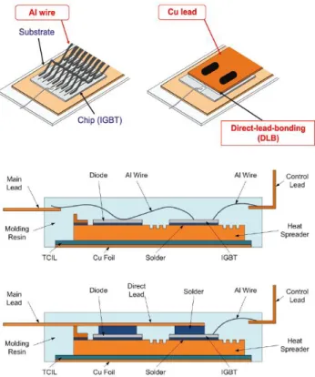
Using wire-bonding (WB) power modules for high current applications (typically up to 600A DC @ Tcase=25°C for a 15x15mm² chip size) requires interconnection with low resistance and inductance values to reduce voltage drop and additional losses. Conventionally, to improve current and losses distribution, we use large diameter copper wires bonding (WB) in parallel. For demanding applications, Direct-Lead-Bonding (DLB) with thick copper clips at the top of chips and assembled inside a compact epoxy molded case are also used.
At first, in §II.A. the two power modules geometries are described and a numerical model, adapted to a finite element study, is presented. In §II.B. to consider, the very high ratio between the thin layers of deposited materials and the
largest volumes of bulk materials, the model uses 3D volume elements as well as 2D surface elements.
In a second time, in part III. we present electromagnetic simulations that have been done in DC and AC (20 kHz) modes to evaluate stray electrical resistances and inductances. Meshing was done by considered the frequency effects (skin and proximity) and the variation of the current density location. Finally, in a third time, in part IV. for the thermal study, we have considered steady and transient modes to calculate thermal losses in chips, thermal losses due to current circulation through wires and clips elements, according to a classical steady state PWM inverter operation mode.
II. POWER MODULES UNDER STUDY
A. Geometries and materials
In Fig.1, we can see the two power modules studied. These modules, whose electrical characteristics are comparable, do not have the same size (WB: 34.5cm2 and DLB: 53.8.0cm2). However, it is mainly their connections that differ and are studied in this article.
Figure 1 : Power modules under study in wire-bonding type (at left) and in copper clip type connection (at right) for EV-HEV application
As we can see in Fig.2, for high current applications, designers multiply large diameter (up to 500μm) bonding wires in parallel (up to 20) and connection areas to improve current and losses distribution. In Direct-Lead-Bonding (DLB) assemblies in epoxy molded case, the chips are soldered on one side on a common lead frame and a dedicated copper clip is soldered or sintered directly on the other side of the chips to provide improved and better reliable electrical connections and an improved power cycling capability.
Figure 2 : The two different WB and DLB interconnections cross section view
B. Equivalent numerical models
To better understand the impact of WB and DLB interconnections from an electromagnetic and thermal point of view, we understand that a 2D model has its limits. Therefore, the move to a complete 3D modeling is necessary if one wants to consider all these phenomena in a realistic way.
In Fig.3, we can see the two 3D digital models that have been defined using Autodesk Inventor© software. With the help of manufacturer's datasheets and a reverse engineering, all the geometric data have been respected with precision. However, to avoid overloading the model, some parts not needed for the study were removed.
Similarly, the very thin layers of deposited materials have been reduced to zero-thickness (2D) surface layers. However, the effective thickness of these layers is still considered in the calculations by means analytical relations.
Figure 3 : Equivalent numerical models for wire-bonding type (at left) and copper clips (a rigtht)
III. ELECTROMAGNETIC STUDY
The calculations presented in this article were done using the Comsol Multiphysics© software that solves coupled electrical, magnetic and thermal problems in 3D. The relevance of the results strongly depends on the accuracy of the geometric model presented previously, the accuracy of the physical parameters of each material and the boundary conditions. A recalibration of certain physical parameters may then be necessary when the results obtained appear aberrant. Finally, as we will see in the next paragraph for AC mode, special attention must be given to the mesh according to the objectives of the study.
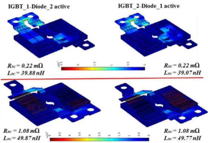
According to Fig.4, stray electrical resistances and inductances were calculated by activating one switching-cell by means of IGBT1 and Diode2.
Figure 4 : IGBT1 & Diode 2 electrically activated (turn-on state)
A. AC mode
In alternative mode, attention must be paid to the mesh to consider the frequency effects that modify the current distribution in the electrical conductors [3]. These frequency effects are skin and proximity effects that reduce the effective section for current flow. Under these conditions, the mesh must be refined in these constriction zones to properly evaluate the current gradients. We have adopted the method of imposing in these zones finite elements whose size is less than half the theoretical skin thickness in copper at 20 kHz (first harmonic current frequency considered through chips).
In Fig.5, we can see the quality of the mesh obtained and the areas where it has been refined. This leads to 2639739 elements and 17981231 DoF for the WB module and 1824095 elements and 12087973 DoF for the DLB module. This size of the problem is not excessive and leads us to simulation times of the order of 15 minutes with a Dell WorkStation 128GB 1866MHz DDR3 ECC RDIMM;
Intel® Xeon® Processor E5-1620 v2 (Quad Core HT, 3.7 GHz Turbo, 10 MB).
Figure 5 : Zoom on the meshing quality in AC study
Fig.6 shows the mappings obtained from current densities. It is verified that at 20 kHz, the current lines are tightened towards the center of the module due to the proximity effect between the two coppers clips of the IGBT and diode chips. For this operating point, we have calculated the values of the electrical resistances and inductances seen from the power terminals. We verify that the DLB solution offers better values than the WB one. Indeed, the copper clips allow reducing the RAC value by one third compared with
the wire-bonding reference. The LAC value is only reduced
by 25%. These values are consistent with those calculated or measured elsewhere [4-5].
Figure 6 : Current density in AC and impedance values
B. DC mode
Simulations in DC mode are easier to do because frequency phenomena are no longer present. The mesh can be simplified and that generated by default by the software is often enough.
Fig.7 shows the new distribution of the current density. It is verified that the current flows this time in the entire conductors and that the values obtained have logically evolved downward for the resistors and upward for the inductors. It is noted again that the DLB solution is better than the WB one. Indeed, RDC value is four times lower than
the reference module. Given the geometrical symmetry of the modules, the dual operating mode (IGBT2 & Diode1) gives us the same results. However, it can be noted that the DLB module is more sensitive to the frequency effect than the wire-bonding module: its RAC increases by 130% at
20kHz while it only increases by 38% for wire-bonding module. The explanation lies in the presence of a massive copper piece while the reference module has a split wire connection.
Figure 7 : Current density in DCand (RDC, LDC) parameters of DLB module (up side)
and wire-bonding module (down side)
IV. THERMAL STUDY
The objective here is to determine the heating of the power modules in a realistic operating mode. In our case, the module operates as a PWM voltage inverter mode, with a switching frequency of 20 kHz and a modulation index of 0.9. It is connected, on the DC side, to a voltage source of 300V and supplies an inductive load (power factor equal to 0.8) at 200A peak-current. Under these conditions, off-line analytic calculations were processed to impose realist electric constraints by means to an effective equivalent RMS (or DC) current of 90A injected through IGBT1&2 chips and 44A through Diode1&2 chips.
To do that, we used a superposition method. First, the electric power density distribution due to 90A circulating current is calculated when the IGBTs are in on-state. In a second time, the electric power density distribution due to 44A circulating current is calculated when Diodes are in on-state. Finally, to calculate the resulting temperature, we evaluated the global power density as the sum of these two contributions without forgetting to impose realistic losses in the IGBTs (190W) and the Diodes (73W). This chip losses have been calculated in off-line by an analytic approach from datasheet parameters only for a constant temperature Tj=125°C.
Concerning the thermal conditions at the boundaries of the domain, we have imposed a realistic value of 10W.m-2.K-1 to take into account the convective and radiative exchanges to the ambient. For the interface with the heatsink on the back side, we imposed a constant temperature of 16 °C corresponding to that of the cooling water.
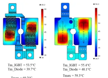
A. Steady state mode
As we can see in Fig.8, the two configurations (clip and WB) have approximatively the same temperature field. The maximum temperature reached in WB is slightly higher than the clip one localized in the IGBT chip. We have notice that maximum temperature points are localized inside the IGBT
for the DLB module, and on the wire bonding for WB module. This result is due to the effect of more punctual contacts of the WB module. However, the misalignment of the copper clips on the chips causes a less homogeneous temperature field than the WB module Also, the global temperature rising is logically due to chips. The difference in temperature is not noticeable between the two modules because most of the heat flow is imposed by the water-cooling system. In Fig. 9, we can see the vertical heat flux distribution. Table 1 and 2 give us the distribution and proportion for DLB and WB modules. As we can see, the majority of the thermal transfer takes place well from the chips to the cooler system but the spreading effect the copper clip is also visible. It can also be seen that the heat flow is reversed between the copper wires and the IGBTs. This is because there is a hot spot in the middle of the copper wires whose temperature is higher than that of the bonding feet.
Figure 8 : Temperature field for the WB module (left) and the DLB module (right)
Figure 9 : Vertical heat flux distribution for the WB module (top) and the DLB module (bottom)
Table 1 : Heat flux proportions (DLB module) Flux direction Value of the flux
IGBT to base plate 185.6 W IGBT to clip 3.95 W IGBT to epoxy 0.12 W Diode to base plate 76.5 W
Table 2 : Heat flux proportions (WB module) Flux direction Value of the flux
IGBT to base plate 186.26 W IGBT to wires -0.34 W (reverse flux) IGBT to epoxy 0.02 W Diode to base plate 60.8 W
In Table 3, we calculated the equivalent thermal resistance between each chip and the cooling system. These values are very close because the assemblies of the chips on their substrate and the cooling system are almost identical between the two modules. Only the connectors (WB or DLB) differ in the upper part where the heat transfer is not significant.
Table 2 : Thermal resistances
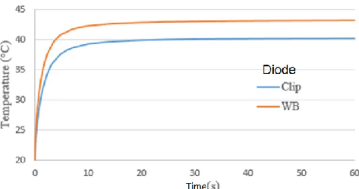
B. Transient mode
The transient study was carried out with a time step of 1ms with the same power conditions. The temperature evolution are quite identical for both configurations due to the same reasons mentioned above concerning an almost identical assembly, below the chip, of the chips on their substrate. In Fig.10, it can also be seen that the time-domain evolution of the average temperature of the chips is almost the same for the two modules. The 95% steady state temperature is reached in less than 10 seconds. DLB module has a slight higher thermal inertia due to the presence of the copper clip which plays the role of thermal capacitance. The effect is minor because few heat flux is injected through this clip and the thermal filtering is very reduced.
Figure 10 : Mean temperature evolution for IGBT and Diode chips
We can also notice a steady-state temperature difference for diodes chips. This is due because diodes used for the two modules WB and DLB are not the same.
V. CONCLUSIONS
In this article, we presented a 3D electro magneto thermal modeling work of two power conversion modules. The goal was to compare two technological solutions for electrical chips interconnections, a traditional solution using wires (WB) and a newer solution using clips (DLB).
We have tried to seek the impact of these two solutions on the electrical impedances (resistances and inductances) which impact the electrical losses and the quality of the commutations, but also on the heating resulting from all the modules which is a significant dimensioning data.
We used a finite element method to finely model the complex and heterogeneous assemblies of the modules. Attention was paid to the definition of the numerical model, the quality of the mesh especially for the frequency study and a realistic study corresponding to a inverter behavior. This study has allowed us to confirm the interest of the DLB solution compared to the WB one, in the electrical point of view. Stray electrical (DC and AC) resistance and inductance values for DLB modules have been significantly reduced compared to the WB one. But DLB module presents more frequency dependence due to its more bulk connections compared with WB ones. This leads to a reduction of the electrical losses and to an improvement of the commutations with using DLB module. From a thermal point of view, the differences are not significant. Indeed, the assembly of the chips on their substrate and their cooling system is almost the same. Under these conditions, the steady-state temperatures and the thermal time constants are equivalent.
This study constitutes an original approach of the 3D modeling of power module. In the future, this modeling will allow us to optimize chip assembly techniques in modules, optimize thermal behavior and electrical interconnections. It might be interesting to study a technological evolution of the DLB structure by introducing a double cooling, above and below the chip.
VI. REFERENCES
[1] T. Ueda, N. Yoshimatsu, N. Kimoto, D. Nakajima, M. Kikuchi and T. Shinohara, "Simple, compact, robust and high-performance power module T-PM (transfer-molded power module)," 2010 22nd
International Symposium on Power Semiconductor Devices & IC's (ISPSD), Hiroshima, 2010, pp. 47-50.
[2] Hidetoshi Ishibashi, Hiroshi Yoshida, Daisuke Murata, Shota Morisaki, Hodaka Rokubuichi, Nobuhiro Asaji, "Direct Power Board Bonding Technology for 3D Power Module Package",
PCIM June 2018, Nuremberg, Germany.
[3] Xiao Zhang, Hui Zhang, Rui-wen Yu, Guo-jun Tan, "Planar bus bar optimum design in high-power converters based on FEM analysis", The 2nd International Symposium on Power Electronics
for Distributed Generation Systems, 16-18 June 2010, Hefei,
China.
[4] Adrien Letellier, Maxime R. Dubois, Joao Pedro F. Trovao, and Hassan Maher, "Calculation of Printed Circuit Board Power-Loop Stray Inductance in GaN or High di/dt Applications", IEEE
Transactions on Power Electronics, Vol. 34, no. 1, January 2019.
[5] Jianjing Wang, Henry Shu-hung Chung and River Tin-ho Li, "Characterization and Experimental Assessment of the Effects of Parasitic Elements on the MOSFET Switching Performance", IEEE