Demonstration of Monolithically Integrated
Graphene Interconnects for Low-Power CMOS
Applications
by
Kyeong-Jae Lee
Submitted to the Department of Electrical Engineering and Computer
Science
in partial fulfillment of the requirements for the degree of
Doctor of Philosophy
at the
MASSACHUSETTS INSTITUTE OF TECHNOLOGY
September 2011
ARCHIVES
OF TECHPITA NO 1ULOIY
SEP 2 7 2011
U BARI E
@
Massachusetts Institute of Technology 2011. All rights reserved.
A uthor ...
...
...
Department Af"Electrical Engineering and
Certified by.
Computer Science
August 19, 2011
...
. . .; ... .. .....
..
*...
Jing Kong
ITT Career Development Associate Professor
Thesis
Ri nrvisorCertified by...
Anantha P. Chandrakasan
Joseph F. and Nancy P. Keithley Professor
Thesis Supervisor
Accepted by...4
ieslidkA
olodziejski
Chair, Department Committee on Graduate Students
Demonstration of Monolithically Integrated Graphene
Interconnects for Low-Power CMOS Applications
by
Kyeong-Jae Lee
Submitted to the Department of Electrical Engineering and Computer Science on August 19, 2011, in partial fulfillment of the
requirements for the degree of Doctor of Philosophy
Abstract
In recent years, interconnects have become an increasingly difficult design challenge as their relative performance has not improved at the same pace with transistor scaling. The specifications for complex features, clock frequency, supply current, and number of I/O resources have added even greater demands for interconnect performance. Furthermore, the resistivity of copper begins to degrade at smaller line widths due to increased scattering effects. Graphene has gathered much interest as an interconnect material due to its high mobility, high current carrying capacity, and high thermal conductivity. DC characterization of sub-50 nm graphene interconnects has been reported but very few studies exist on evaluating their performance when integrated with CMOS. Integrating graphene with CMOS is a critical step in establishing a path for graphene electronics.
In this thesis, we characterize the performance of integrated graphene intercon-nects and demonstrate two prototype CMOS chips. A 0.35 prm CMOS chip imple-ments an array of transmitter/receivers to analyze end-to-end data communication on graphene wires. Graphene sheets are synthesized by chemical vapor deposition, which are then subsequently transferred and patterned into narrow wires up to 1 mm in length. A low-swing signaling technique is applied, which results in a transmitter energy of 0.3-0.7 pJ/bit/mm, and a total energy of 2.4-5.2 pJ/bit/mm. We demon-strate a minimum voltage swing of 100 mV and bit error rates below 2x10-. Despite the high sheet resistivity of graphene, integrated graphene links run at speeds up to
50 Mbps. Finally, a subthreshold FPGA was implemented in 0.18 pm CMOS. We
demonstrate reliable signal routing on 4-layer graphene wires which replaces parts of the interconnect fabric. The FPGA test chip includes a 5x5 logic array and a TDC-based tester to monitor the delay of graphene wires. The graphene wires have 2.8x lower capacitance than the reference metal wires, resulting in up to 2.11x faster speeds and 1.54x lower interconnect energy when driven by a low-swing voltage of 0.4 V. This work presents the first graphene-based system application and demonstrates the potential of using low capacitance graphene wires for ultra-low power electronics.
Thesis Supervisor: Jing Kong
Title: ITT Career Development Associate Professor Thesis Supervisor: Anantha P. Chandrakasan Title: Joseph F. and Nancy P. Keithley Professor
Acknowledgments
I will praise the LORD, who counsels me; even at night my heart instructs me. I keep my eyes always on the LORD.
With him at my right hand, I will not be shaken. Psalm 16:7-8
Thank you Jesus, my rock and my fortress.
First, I sincerely thank my two advisors, Professor Jing Kong and Professor Anan-tha Chandrakasan. Your advice and support has made this work possible. Thank you for giving me this research opportunity and being patient with this project. I thank Jing for her kindness, openness, and continuous encouragement. I have learned how to maintain the right perspective on all matters, which extends far beyond research. I thank Anantha for his dedication, passion, and continuous support. Anantha is truly one of the best at identifying the problem and providing direction and motivation. I have learned a great deal from both of you.
I am also very grateful to my thesis committee member, Professor Tomas Palacios.
Tomas has given this work a great deal of attention and support. Thank you for your enthusiasm and interest in this thesis. Your feedback and support has made this thesis better.
This work has also greatly benefited from the research of current and past stu-dents. I thank Mario Hofmann for helping create the RF probe mounts for the first test chip. I am also grateful for many of the discussions we have had over the years. I also thank Hyesung Park for assisting part of the graphene transfer work. I am grate-ful for Masood Qazi for discussing circuit design and testing issues. I also thank my co-workers, especially Allen Hsu, Kikang Kim, Yongcheol Shin, Soomin Kim, Sungmi Jung, Minseok Choi, Wenjing Fang, Roman Caudillo, Helen Zing, Alfonso Reina, Daniel Nezich, Hootan Farhat, Jikang Yuan, Marek Zebrowski, Ervin Miles, Sreekar Bhaviripudi, Stefan Thiele, Ya-Ping Hsieh, Xiaoting Jia, Federico Villalpando Paez, Liming Xie, Paulo Araujo, Daniela Mafra, Xialoing Shi, Ying Feng, Yumeng Shi,
Kai Zhang, Ehdi Burcombe, Vitor Manfrinato, Pan Tao, Taegsang Cho, Pat Mercier, Marcus Yip, Courtney Schmitt, Fred Chen, Daniel Finchelstein, Vivienne Sze, Joyce Kwong, Sunghyun Park, Sungjae Ha, Sunghyuk Lee, and Mahmut Sinangil. I espe-cially thank all the students who have dedicated their time and effort in maintaining many of the equipments in the Jing Kong lab.
I am thankful for the SRC/FCRP Interconnect Focus Center for providing me with funding support during most of my Ph.D. Attending workshops and the annual review sessions was always a great learning experience.
I also thank Lin Zhu and Yuri Dagaev for their friendship, support, and prayers.
Finally, I thank my family, without whom I would never have accomplished all these things. Thank you for your support, love, and prayers. I love you all very much.
My parents, Jong-Kun Lee and Soyeon Mah, have given me endless encouragement
and inspiration. I am deeply blessed to know that you will always be a source of comfort and strength for me. I am very grateful for my brother, Seong-Jae, whom I greatly admire. Your support is often without many words, but your presence and support is always felt.
I am also blessed to have the support of a second set of parents, Seunghee Lee
and Insun Kim. Thank you for your love and prayers. In particular, the past year has been difficult, but your encouragement has made me strong. I also thank Ye-eun for her kind support.
I am deeply grateful to my wife, Ye-ryoung. Your presence, love, and prayers have
made our time at MIT meaningful. Except for our research projects, it truly has been my joy to have been able to share all this experience with you. This work has finally come to fruition because of your joyful smiles and patience. You deserve most of the credit. Thank you for your support. I love you very much.
Contents
1 Introduction
1.1 Interconnect Challenges . . . .
1.2 Thesis Contributions . . . .
2 Benchmarking Graphene Interconnects
2.1 Modeling Graphene Interconnects ...
2.1.1 Physics-Based Circuit Models . . . . 2.1.2 M ultilayer Stacks . . . .
2.1.3 Mean Free Path and Line-Edge Roughness... 2.2 Modeling Copper Interconnects . . . .
2.3 Comparison of Copper and Graphene Interconnects . . . . 2.3.1 Sheet Resistivity . . . .
2.3.2 Wire Resistance and Capacitance . . . . 2.3.3 Interconnect Performance for Subthreshold Circuits 2.4 Sum m ary . . . .
3 Fabricating Graphene Devices
3.1 Survey of Existing Methods . . . .
3.2 Fabrication of Graphene Wires . . . . 3.2.1 Synthesis of Graphene Sheets . . . .
3.2.2 Substrate Transfer and Graphene Patterning . . . . 3.3 Monolithic Integration with CMOS . . . .
3.3.1 A 0.35 pm CMOS Prototype . . . ... 25 . . . . . 25 . . . . . 25 . . . . . 30 31 . . . . . 34 36 . . . . . 36 38 . . . . . 43 . . . . . 48 49 49 52 52 53 55 56
3.3.2 A 0.18 pm CMOS Prototype . . . . 3.3.3 Optimizing Process Flow . . . . 3.4 Summary . . . .. . .
4 Characterizing Multilayer Graphene Devices
4.1 Sheet Properties . . . .. 4.2 Wire Properties . . . ..
4.3 Breakdown Current Density . . . . 4.4 Summary . . . .. . . .. . ..
5 Graphene Data Links
5.1 Overview . . . .
5.1.1 Implementation of Low-Swing Data Links
5.1.2 Experimental Setup . . . . 5.2 Measured Results . . . . 5.2.1 Delay Performance . . . . 5.2.2 Energy Performance . . . . 5.2.3 Limitations . . . . 5.3 Summary . . . .
6 Field-Programmable Gate Array 6.1 Designing a FPGA . . . . 6.1.1 Chip Architecture . . . . 6.1.2 Interconnect Architecture 6.1.3 Graphene Tester . . 6.2 Testing Methodology . . . . 6.2.1 Hardware Setup . . . . . 6.2.2 Software Flow . . . . 6.3 Measured Results . . . .
6.3.1 TDC and Graphene Teste
6.3.2 System Energy... using Graphene . . . . . . . . .. . . . . . . . . . . . . . . . . . . . . . . . . . r . . . . 75 75 76 . . . . 78 Wires 89 89 90 92 97 101 103 105 109 109 113
. . . .
..
. . . .
6.3.3 Comparison of Graphene and Metal Wires . . . 117 6.3.4 Limitations . . . 119 6.4 Summary . . . 121 7 Conclusions 123 7.1 Summary of Results . .. . . . 123 7.2 Concluding Thoughts . . . 124
List of Figures
2-1 Equivalent circuit model for a graphene wire . . . . 26
2-2 Diagram of zigzag and armchair configuration for graphene wires. . . 27 2-3 Number of conduction channels in a graphene nanoribbon. . . . . 29
2-4 Calculated mean free path in a graphene nanoribbon. (a) A constant AD=1pm is assumed while varying the Fermi level. (b) A constant
EF=0.21 eV is assumed while varying scattering probability. . . . . . 33 2-5 Mobility of graphene wires vs. wire width. Data points are from [43]
and lines represent calculated mobility. . . . ... 34
2-6 Sheet resistance of various graphene samples . . . . 37 2-7 Sheet resistance of graphene and Cu. Data points are measured results
from [55].... . . . . . . . 38 2-8 Cross section of interconnect and surrounding ground planes. The
dielectric constant is r,=2.2 and the aspect ratio is 2 for Cu wires. The estimated height H of the graphene wire is the product of the interlayer spacing 0.34 nm and the number of layers. . . . . 39 2-9 Resistance per unit length. (a) Graphene is calculated as the limit on
SiO2. Cu model assumes ITRS projection where (peu=0.95,Res=0.45,LER=0,
H=2xW). (b) zigzag graphene assumes EF=0.2eV, AD=1 puum, Pc=0.5. Cu model assumes experimental values from [72] where peu=0,Res=0.79, and LER=14nm. . . . . 40 2-10 Capacitance of graphene and Cu wires. Cu wires assume a constant
2-11 Wire capacitance as a function of number of graphene layers. Wire width is fixed at 10 nm. Cu wire assumes an aspect ratio of 2. .... 42 2-12 Wire resistance as a function of number of graphene layers. Wire width
is fixed at 10 nm. Cu wire assumes an aspect ratio of 2. . . . . 42
2-13 RC delay as a function of number of graphene layers. Wire width is
fixed at 10 nm. Cu wire assumes an aspect ratio of 2. . . . . 43 2-14 Wire capacitance as a function of aspect ratio. As the aspect ratio
increases, the height of the Cu wire increases or more layers of graphene is used... .. ... ... ... 45
2-15 Wire resistance as a function of aspect ratio. . . . . 46
2-16 Diagram of CMOS inverter driving a distributed RC wire. . . . . 46 2-17 Equivalent 7r3 RC wire model used for simulating a distributed RC
wire with total resistance R, and total capacitance C .. . . . . 47
2-18 Performance of graphene and Cu wire in subthreshold. . . . . 47
3-1 Diagram of CVD process. Substrate is placed in a thermal furnace where a mixture of hydrogen and methane flow at 10000C. . . . . 54
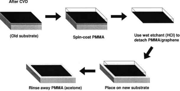
3-2 Process flow for transferring graphene film on to an arbitrary target substrate... . . . . . . . . 54
3-3 Process flow for fabricating graphene wires . . . . 55
3-4 Process flow for graphene and CMOS integration. A drawing and optical image at one end of the graphene wire is shown. . . . . 57 3-5 Process flow for synthesizing/transferring graphene sheets and
inte-grating graphene wires with the CMOS test chip. . . . . 59
3-6 Image of graphene wires on top of the CMOS chip. We observe
ar-eas of (a) uniform 4-layer wires, as well as (b) uniform and non-continuous regions due to wrinkling and tearing that occurs during the transfer process. . . . . 60
4-1 Optical image of graphene sheets on Si substrate with 300 nm SiO2 (SiO2/Si). Dark colored regions represent thicker graphene layers.
Scalebars are 10pm. . . . . . 64
4-2 Estimated area coverage of 1-3 graphene layer regions. . . . . 65
4-3 Average roughness of graphene sheets. .... ... 65
4-4 Measured sheet resistance. . . . . 66
4-5 Height distribution of graphene (CH4=1.7%) from AFM measurements. Inset shows optical images of fabricated graphene wires. . . . . 67
4-6 Resistance of graphene wires fabricated on SiO2/Si test wafers. ... 68
4-7 Measured I-V curve of a 50 pm long graphene wire undergoing electrical breakdown. Insets show an optical image of the graphene wire before and after the measurement. . . . . 69
4-8 Measured I-V curve of a 10 pm long graphene wire undergoing electrical breakdown. Insets show an optical image of the graphene wire before and after the measurement... . . . . . 70
4-9 Measured maximum breakdown current density as a function of resis-tivity. The resistivity is defined at the point just prior to breakdown, as in [28,105]... . . . . . . . . . . . 70
4-10 Measured electrical field at the point of current breakdown. . . . . 71
4-11 Measured average breakdown current density wire length. The error bars plot the standard deviation of JMAX at each length. . . . . 72
4-12 Measured maximum breakdown current density as a function of resis-tivity... . . . . . . . . 72
5-1 Overview of chip. Graphene wires are monolithically integrated and electrically connected to a transmitter and receiver. The low-swing topology uses a sense-amplifier (SA) at the receiver. . . . . 76
5-2 (a) Diagram of low-swing design. The graphene wire is simulated as a r3 distributed RC wire. (b) Waveform of simulated low-swing design using VDD= 3.3V, VREF=0.6V, RGR=180kQ, CGR=200fF, and
CINTEG= 3fF. . . . . 77
5-3 Diagram of experimental setup. . . . . 78
5-4 Photo of experimental setup... . . . . . . 78 5-5 SEM image of CMOS die and integrated graphene wire.... . . .. 79 5-6 Transient waveform of digital signals for the low-swing design with a
231-1 PRBS input pattern (VDD=3.3V, VREF=0.5V). ... 80
5-7 Measured delay (top) and bit error rates (bottom) of a low-swing
graphene channel. The clock delay (Aclk) is fixed at 12.8 ns. The BER is measured using a 231-1 PRBS at VDD=3.3V . . . . 81
5-8 Minimum operable VREF... 82
5-9 Histogram of delay measurements (L=0.5 mm) at VDD= 3.3V. For the
low-swing design, the data plotted is at VREF=1 V, where the channel delay is minimized.. . . . . . . . . 83 5-10 Measured channel delay of graphene wire in a full-swing topology. . . 83 5-11 Measured channel delay of graphene wire in a low-swing topology
(L= 0.5 m m ). . . . . 84 5-12 Measured energy profile of graphene wire. . . . . 85 5-13 Comparison of measured and simulated energy profile of a low-swing
data channel at VDD= 3.3V. The data points are measured values,
whereas the solid lines are from simulations using values of RGR=90
kQ, CGR=115 fF, and CINTEG= 3 fF. . . . . 86
6-1 Overview of FPGA test chip. Graphene wires are integrated on top of the CMOS chip and interface to the switch matrices (SW). . . . . 91 6-2 Implementation of Configurable Logic Blocks (CLB). Each CLB
6-3 Diagram of a conventional switch matrix. At each intersection, six
NMOS pass transistors are used.... . . . . . . . 93
6-4 Implementation of programmable switch matrix (SW). (a) Only the North-West connections are shown. (b) All connections are shown. . . 95
6-5 Diagram of graphene interface. Graphene is used to replace the hor-izontal double-length (L=2) wires. Each L=2 segment includes 3 re-dundant graphene wires and one reference (M5) wire. A TDC-based tester measures the delay (between A-B) for each wire.. . . . . . 96
6-6 Implementation of low-swing driver and receiver . . . . 97
6-7 Schematic of delay unit in TDC. . . . . 98
6-8 Simulated resolution of delay unit in TDC. . . . . 99
6-9 Simulated histogram of TDC vs. VDD --- ---... -. 100
6-10 Simulated histogram of TDC vs. VCTL -.-.-... ... 100
6-11 Schematic diagram of TDC. Each buffer has a delay equal to r. . . . 101
6-12 Simulated waveform of graphene tester.... . . . . . . 102
6-13 Relationship between TDC code and absolute delay. . . . . . . . 102
6-14 Diagram of experimental setup. A commercial Xilinx FPGA is used as a master device to configure the test chip and run benchmarks. . . 104
6-15 Photo of experimental setup. The test chip is wire-bonded to a pin-grid array package. . . . . 104
6-16 CAD flow for generating a bitstream from a Verilog source. . . . . 106
6-17 Resource utilzation of various benchmarks. . . . . 108
6-18 Measured waveforms from logic analyzer while running two example benchmarks: a (a) 3-stage pipelined multiplier and a (b) 4-to-16 decoder.109 6-19 Image of 0.18 pm CMOS test chip and integrated graphene wires. . . 110
6-20 Measured results (data link delay) from the TDC-based tester for (a) graphene and (b) reference (M5) wires. . . . 110
6-21 Histogram of L=2 wire delay measured from testers at various supply voltages... . . . . . .. 111
6-23 Measured TDC energy per conversion. . . . . 112 6-24 Measured TDC energy as a function of supply voltage. . . . . 113 6-25 Measured power consumption of chip (a) at various run modes and
when (b) system is idle. . . . . 114
6-26 Measured total energy of FPGA chip. . . . . 115 6-27 Performance of various benchmarks at VDD=0.4 5 V. . . . . 116 6-28 Measured (a) maximum operating frequency and (b) L=2 wire
en-ergy (from VREF) while running a representative benchmark (3-stage pipelined multiplier) and enabling the graphene wires. Labels indicate relative system performance when M5 wires are enabled (not shown in figure). . . . . 117 6-29 Measured (normalized) (a) maximum operating frequency and (b) L=2
wire energy of the system when graphene wires are enabled. The data points are normalized to the case when M5 wires are enabled. . . . . 118 6-30 Breakdown of measured power consumption when system is (a) running
List of Tables
3.1 Summary of graphene performance from various fabrication methods. 52 5.1 Summary of measurements. . . . . . . . . . 87 6.1 Summary of benchmark applications. . . . . 108 6.2 Summary of FPGA test chip. . . . . 120
Chapter 1
Introduction
1.1
Interconnect Challenges
The semiconductor industry has advanced at an exponential rate over the last few decades. In recent years, interconnects have become a major limiting factor on the performance of very large-scale integrated (VLSI) systems [1-3]. The relative perfor-mance of interconnects has not improved at the same pace with transistor scaling [2]. Latency, energy dissipation, and signal integrity have all become an increasingly diffi-cult problem to cope with. With shrinking cross-sectional areas and hence increased electrical resistance, the interconnect delays have begun to exceed transistor delays and this trend worsens at advanced technology nodes [2,4]. While the capacitance of a global wire remains fairly constant under technology scaling, the addition of more complex features has resulted in higher energy dissipation. Global wires often dominate the total power consumption in many VLSI systems [5,6]. Furthermore, the specifications for clock frequency, supply current and voltage, number of I/O re-sources has added greater demands for higher levels of integration and interconnect performance [7].
Many solutions have emerged to address these challenges, ranging from new ma-terials and processes to novel micro-architectures. At the system level, multi-core systems has emerged as a recent trend, where slower data transfers are managed across multiple dies and faster local communication is kept on-chip [8,9].
Nonethe-less, for high bandwidth systems, cross-chip communication can still limit total per-formance as it increases on-die cache delays and buffer resources. Three dimensional integration can also benefit certain applications as the length-reduction in wires leads to lower energy dissipation [10, 11]. Heat removal and I/O resource allocation re-mains a challenge for such integration schemes. Innovative circuit techniques have also contributed to more efficient data communication. On-chip transmission lines have shown near speed-of-light latency and high throughput, but this comes at the cost of significant wire resources [12-14]. Low-swing signaling methods reduce the voltage level primarily as a power-reduction technique, but often have higher latency and reduced noise margins [15-18]. Other solutions have combined CMOS repeaters with channel equalization techniques.
Furthermore, innovative device structures or new nano-materials have already found their way into prototype VLSI applications in an effort to reduce power dissi-pation [19, 20]. Improving fundamental material properties are expected to become more important in highly scaled technologies. At narrow line widths, surface scatter-ing of conductscatter-ing electrons are projected to be a major concern, drastically increasscatter-ing the effective resistivity of copper interconnects [21, 22]. This results from a combi-nation of smaller cross-sectional dimensions and increased liner thicknesses. Heat management will also be increasingly important, as higher energy dissipation of wires and poor thermal conductivity of low-K insulators contribute to substantial temper-ature increases.
Among many materials, carbon-based materials such as graphene or carbon nan-otubes have received much attention in recent years as a replacement for copper interconnects. Graphene is a planar sheet composed of carbon atoms. Graphene exhibits ballistic transport [23,24], high intrinsic mobility [24,25], high thermal con-ductivity [26,27], and high current carrying capacity [28-30], making it attractive not only for transistors [31, 32] but also for interconnects [33, 34] and even as a thermal interface material [35]. Theoretical projections show that at small line widths (< 8nm), graphene will outperform copper with a 1:1 aspect ratio [33].
a cylindrical tube. Graphene and carbon nanotubes share many excellent properties but graphene is more attractive from a manufacturing standpoint. Carbon nanotubes are chemically stable but it is extremely difficult to control their size and placement. Graphene can be grown in large sheets [36,37] and then be subsequently patterned and etched using standard lithography methods. This results in better control and higher reproducibility of graphene devices.
Despite these excellent properties, the fabrication process is not well controlled at the level required for integrated circuits. Befittingly, the majority of graphene research focuses on methods to improve the material quality or finding innovative device ar-chitectures. To explore the full potential of graphene-based electronics, the research focus must extend beyond materials and devices. We need to find new promising applications and understand their requirements throughout all phases of the design from material to system. One of the major advantages of graphene over other nano-materials is that graphene can be lithographically processed. This allows an easy path toward integration with existing silicon technology. DC characterization of sub-50nm graphene interconnects has been reported [28, 34], but very few studies exist on evaluating their performance when integrated with CMOS. Integrating graphene with CMOS is a critical step in establishing a path for graphene electronics. Chen et al. have reported the first integrated graphene/CMOS system [38]. They use CMOS ring oscillators to indirectly measure the performance of short graphene wires. More importantly, studying the performance of graphene under real workloads is needed but demonstration of a full system using graphene has not been made. Although sev-eral reports exist on graphene applications [32,39,40], these are gensev-erally prototypes that have limited functionality and only use a few devices. Developing a complete graphene-based system not only helps establish graphene as a viable interconnect ma-terial but also provides a general roadmap for mama-terial, circuit, and system design.
1.2
Thesis Contributions
The objectives of this thesis are to characterize the performance of graphene in-terconnects and demonstrate a complete graphene/CMOS application. This thesis
contributes in the following areas:
(1) Monolithic Integration with CMOS.
Providing a path toward integration is critical in establishing the use of graphene as interconnects. Here, we demonstrate monolithic integration of graphene with
CMOS on two prototype test chips. The purpose of the first test chip is to
characterize the performance of long graphene wires. Off-chip measurements have limited scope and often require expensive equipment. The first test chip provides a platform to directly measure the delay and energy associated with driving a signal on long graphene wires. The second test chip demonstrates a complete system application. Large sheets of graphene are synthesized and then transferred to the CMOS chip. We then use standard lithography steps to pattern narrow graphene wires and connect them with the underlying CMOS
circuitry. Details of the process flow are outlined in Chapter 3.
(2) Characterization of Multilayer Graphene Interconnects.
In this work, we grow large-area graphene sheets by chemical vapor deposi-tion [36, 37, 41, 42]. The underlying catalyst film differs among the various growth methods, but Cu foils are a popular choice since they yield highly uni-form monolayer graphene sheets [41,42]. However, the monolayer sheet needs to be transferred multiple times to achieve a lower sheet resistance. In con-trast, the use of Ni catalyst films generally produces a thick multilayered stack of graphene sheets and does not require multiple transfers. Both methods are used throughout this thesis. Here, we apply the term 'multilayer' to indicate graphene sheets with more than 10 layers. While graphene interconnects us-ing monolayer and few-layer sheets have been previously characterized [34,43], no studies exist on using thick multilayer graphene sheets as interconnects. In
this thesis, we conduct both off-chip and on-chip measurement of multilayer graphene interconnects. We characterize the properties of multilayer graphene sheets as well as long graphene wires. We implemented a CMOS test chip onto which 1 mm length graphene wires are monolithically integrated. Unlike Chen's work [38], this test chip focus on end-to-end data communication on medium to long multilayer graphene wires. The performance of each graphene wire is measured in detail, using isolated transmitters and receivers.
(3) Demonstration of Graphene-based Subthreshold System.
The analysis and results from Chapter 2 and Chapter 5 point to the large wire resistance as a major limitation for using graphene for high-speed communica-tion. Unless very thick stacks of high quality graphene layers can be fabricated, the sheet resistance of a multilayer stack cannot match that of a Cu wire. In-stead, another way to leverage graphene wires is to fabricate ultra-thin wires which have low wire capacitance. The low capacitance of few-layer graphene devices offers great opportunities for ultra-low power applications, which of-ten have moderate frequency requirements. In Chapter 2, we briefly discuss this trade-off between speed and energy and suggest that ultra-thin graphene wires can provide significant energy reduction in subthreshold applications. Fur-thermore, we develop a second CMOS chip that operates in subthreshold and takes of advantage of few-layer graphene interconnects. This test chip presents the first experimental demonstration of a system application using graphene de-vices. Graphene is monolithically integrated as part of the interconnect fabric in a field-programmable gate array (FPGA). An FPGA has a highly interconnect-centric architecture making it an ideal test vehicle for graphene integration. Interconnect delay is a significant portion of the delay due to multiple routing segments in an FPGA. Furthermore, global interconnects have been shown to dominate the total power consumption in FPGAs [5,6].
This thesis is organized as follows. Chapter 2 describes a physics-based circuit model for graphene and compares its performance with Cu interconnects. In
Chap-ter 3, we discuss various graphene synthesis methods and outline the process flow used in this work. The monolithic integration process is also explained. Next, we describe the characteristics of multilayer graphene sheets and wires in Chapter 4 and present the results for integrated graphene data links in Chapter 5. Chapter 6 then explains the FPGA architecture and measured chip results. Finally, Chapter 7 concludes the thesis.
Chapter 2
Benchmarking Graphene
Interconnects
Graphene has large conductivity and large current capacity making them attractive for interconnect applications. Many reports highlight the potential of graphene but experimental results show that the resistivity of graphene is still quite larger than that of Cu. This chapter uses a physics-based circuit model to project and compare the performance of graphene and Cu interconnects.
2.1
Modeling Graphene Interconnects
2.1.1
Physics-Based Circuit Models
An accurate model is needed in order to benchmark the potential performance of graphene interconnects. Here, we use the well known physics-based model presented
by Naeemi et al. [33,44,45]. Figure 2-1 shows the equivalent circuit model for
quan-tum wires including graphene or carbon nanotubes [46]. The value of the circuit parameters depend on the electronic band structure of the material.
When a net current exists in a quantum wire, the kinetic energy of the electrons
(1/2L 2) manifests itself in the kinetic inductance LK. This can be observed at high
Metal
~j]
contacts
graphene W Roonact RQ / 2 dx R0 / 2 Rwa R Cdx Lmdx L dxCodx
CxFigure 2-1: Equivalent circuit model for a graphene wire.
and carbon nanotube devices, the kinetic inductance is usually much larger than the magnetic inductance. For most practical dimensions, the frequency at which the inductive effects begin to be important is usually in the THz range or in some cases several hundreds of GHz. This is well beyond the practical range for most applications and hence will not be considered throughout this thesis. In addition, the wires are assumed to be long enough compared to the mean free path that the contact resistances can be ignored. Contact resistances as small as a few hundred ohms is reported [47,48]. Although the contact resistance is expected to rise at smaller line widths, the exact values also depend on the fabrication process and are difficult to precisely model.
The quantum resistance, quantum capacitance, and kinetic inductance are deter-mined by the total number of conduction channels in the device, which is in turn determined by the chirality and width of the graphene device. The chirality, or con-figuration, of the graphene ribbon depends on the pattern of the edge which can be in an armchair or zigzag configuration (Figure 2-2). While all zigzag edged graphene
devices are metallic, an armchair device may be metallic or semiconducting. An arm-chair device is metallic if the number of carbon atoms across its width is 3p+2, and semiconducting if the number is 3p or 3p+1, where p is an integer.
Zigzag
Armchair
edge
edge
Figure 2-2: Diagram of zigzag and armchair configuration for graphene wires.
The electrostatic capacitance CE is determined by the surrounding materials and geometry. In addition to CE, in a quantum system one must add an electron at an available quantum state above the Fermi energy due to the Pauli exclusion princi-ple. This additional extra energy cost can be equated with an effective quantum capacitance. This quantum capacitance CQ can be expressed as:
4e2
CQ
= hvfNeNh ~ (200aF/ym) Nh (2.1)where e is electron charge, h is the Plank constant, Vf is the Fermi velocity in graphene
(~ 8 x 10⁵m/s), and Neh is the number of conduction channels. Similarly, the quantum resistance RQ is the resistance of an ideal quantum wire with no scattering and equals [49]:
RQ h/2e2 12.9kQ(
Nch Neh
In virtually all practical wires, electrons will get scattered by phonons, defects, and rough edges. The scattered resistance per unit length is rec = RQ/Aeff where Aeff
capacitance of the wire then becomes: R =ot = RQ + rsc (2.3) = RQ 1+ (2.4) Aef f C =ot = CQ//CE (2.5)
=
CQCE(2.6)
CQ+CEBoth the conductance (or 1/R) and quantum capacitance scale linearly with the number of conduction channels. The number of conducting channels or modes is a function of the chirality and width of the device and can be expressed using Fermi-Dirac statistics as:
Neh = Nch,electron + Nch,hole (2.7)
-z1
-E1neexp r kB EF1 +) x EF-Enhole~ 28
e iecro B x / kBT +
where En,eectron (En,hole) is the minimum (maximum) energy of the nth conduction (valence) subband, EF is Fermi energy, kBT is thermal energy, and n is an integer. Using a tight-binding approximation, the subband energy can be calculated as [44]:
hvf
En =
In±+
# (2.9)2W
where
#
is 1/3 and 0 for semiconducting and metallic devices respectively. Several modifications need to be made to this equation especially when the line width be-comes very small. When graphene is patterned into small ribbons, this geometric confinement causes the electronic band structure to change. In reality, the carbon atoms at the edge are spaced slightly closer than the atoms in the middle [50].This shifts the subbands, but most importantly, this opens up a gap in metallic 3p+2 arm-chair devices, which was experimentally verified in [51]. For zigzag graphene ribbons, a small gap also appears due to the staggered sublattice potential from magneticor-dering. The simple tight-binding models are accurate unless graphene ribbons that have a narrow width (< 5 nm) and low Fermi energies. The exact equations are found in [44]. 10 -- Armchair (3p+1) z - Armchair (3p) C .0 10 0 100 3 10 100 Width (nm) 1000
Figure 2-3: Number of conduction channels in a graphene nanoribbon.
Figure 2-3 shows the number of conduction channels as a function of graphene width based on the equations above. We chose an arbitrary Fermi energy value of 0.21 eV. Although the exact number of conduction channels depends heavily on the Fermi energy, the qualitative results do not change. The effect of varying the Fermi energy is discussed in the next section. In Figure 2-3, at large widths, the difference between semi-conducting and metallic devices disappears. As the width decreases, the band gap opening becomes more pronounced. For armchair graphene wires, semicon-ducting ribbons have larger quantum conductances compared to metallic wires, which appears counter intuitive. The reason behind this is that there are smaller gaps be-tween subbands in semiconducting devices than those in metallic ones. Thus, depend-ing on the Fermi energy, more subbands may be populated in semiconductdepend-ing devices. Graphene nanoribbons with rough edges all become semiconducting [47,52,53], which
may not be problematic for interconnect applications since semiconducting wires con-duct as well as metallic wires. [47] suggests that the detailed edge structure plays a more important role than crystallographic direction in determining the properties of GNR. Theory supports this and predicts the energy gap depends sensitively on the boundary conditions at the edges.
The difference between work functions of graphene and the substrate causes some charge to get trapped at the interface [52,54]. This causes the Fermi energy to shift from zero, where EF of 0.13 eV [55], 0.21 eV [52], and 0.4 eV [54] have been previously observed. The shift in EF is associated with the surface charges at the interface rather than the carrier concentration of the substrate. Wang et al. have observed that the conductance per layer saturates as the number of graphene layers increases which suggests that the conduction of graphene sheets is limited by the substrate [48]. A nominal value of EF=0.2 eV is assumed in this chapter.
2.1.2
Multilayer Stacks
The model presented in the previous section assumes a monolayer graphene intercon-nect. Multilayer graphene wires can offer lower resistance, and ultimately, a thicker stack is more reliable for large-scale manufacturing. Depending on the stacking or-der, a multilayer stack of graphene turns in to graphite and the increased intersheet electron interactions lower the conductivity per layer [56]. Therefore, to take full advantage of multilayer graphene devices, the adjacent graphene layers must be non-interacting and electronically decoupled.
To date, the interaction between monolayer and multilayer flakes of graphene is not well understood. Some groups have provided theoretical and experimental evidence suggesting that the transition from graphene to graphite occurs around seven to eight layers of graphene [57,58]. Zhou et al. have suggested that epitaxial graphene behaves as bulk graphite beyond five layers [54]. In contrast, others have demonstrated electronically decoupled multilayer graphene films [37,59] which shows great promise.
effect on the analysis of graphene wires. Xu et al. assumes that the multilayer graphene device is neutral (EF=OeV) and extracts the mean free path from conduc-tivity values of bulk graphite [60]. This results in overly pessimistic projections of multilayer graphene devices compared to Cu wires. In contrast, Tanachutiwat and Wang models the Fermi level shift resulting from multilayer stacks of graphene [61] and conclude more favorable results for multilayer graphene interconnects than Xu et al.
Throughout this chapter, we assume that each adjacent layer is decoupled [37,59] and assume each layer has the same parameters (i.e., EF, Psc, Aeff, etc) that is equal to that of a high quality monolayer graphene device. Although this assumption can be readily validated for few-layer graphene wires (under -10 layers) [37,57-59], for high-performance applications, potentially hundreds of layers are needed to match the resistance of Cu wires.
2.1.3
Mean Free Path and Line-Edge Roughness
Rough edges can backscatter electrons and lower the effective mobility or mean free path. The detrimental effects of line-edge roughness have become more pronounced as the width of nano-scale devices continue to shrink. Controlling the edge of a graphene device is even more important since a rough edge occurs even when a single atom is displaced on the edge of a graphene wire. Recently, Ni nanoparticles have demonstrated the cutting and precise patterning of graphene devices [62]. Although this process achieves the atomic precision necessary to control the edge of a graphene device, this method lacks the control required for large-scale manufacturing. We must assume that some degree of backscattering will occur in the device, as smooth edges are extremely difficult to achieve if not impossible.
Experiments show that the intrinsic mean free path in graphene is in the pm range
[25]. The mean free path of electron-phonon scatterings in graphene nanoribbons is
expected to be extremely large and on the order of tens of pm [63] and hence has little effect on the overall mean free path. The effective mean free path can then be
modeled as [44]:
1 1 1
= + (2.10)
Aeff AD Aedge
where the AD is the mean free path due to the substrate-induced disorders and defects and Aedge is the mean free path associated with the edge roughness. Here, AD is as-sumed to be 1 pm, where a value between 400 nm and 1.2 pm have been demonstrated experimentally [25,52, 64]. The mean free path associated with the edge roughness for the nth subband becomes [32,33,52]:
A =W EF 2
Aedge,n
~ -
1
(2.11)
Pc is the backscattering probability and has a value between 0 and 1. A value of
PSc=0 indicates that the device has a smooth edge and no backscattering occurs,
and P8c=1 indicates that transport along the edges is fully diffusive. The equation
above also indicates that Aedge is proportional to the width of the device. This width dependence was similarly modeled in [60].
Figure 2-4 shows the calculated mean free path. The graphs shows that the mean free path decreases at smaller line widths only when Pc 0 (i.e., when backscattering occurs). The roll off can occur at much smaller line widths depending on the Fermi energy or backscattering probability. Therefore, the resistance of the graphene wire can be improved by increasing the Fermi energy or by fabricating graphene devices with smoother edges. The Fermi energy can be modulated by electrostatic gating or
by means of chemical doping.
Yang and Murali have experimentally demonstrated mobility degradation in graphene nanoribbons as a function of the device width [43]. The mobility is limited by edge scattering at smaller line widths as expected. Using the equations in this section and in 2.1.1, we can extract the mobility of a graphene device as / = 1/engrpgr where ng, and Pgr are the carrier density and effective resistivity, respectively.
Figure 2-5 plots the data from [43] and the calculated mobility assuming a mono-layer armchair wire with Pc=0.5 and ngr=5x1012 cm-2. Typical carrier densities
Fermi Energy
0 0.1 C I- E =0.1IeVS0.01
P =0.2 se 10 100 1000 Width (nm) (a) P =0 Sc(reflective edge)
E
P =0.2
Backscattering
a 0.1 Sc ProbabilityU-!
0.01
P =1(diffusive edge)
EF=0.
2eV
10
100
1000
Width (nm)
(b)
Figure 2-4: Calculated mean free path in a graphene nanoribbon. (a) A constant
AD=1Pm is assumed while varying the Fermi level. (b) A constant EF=0.21 eV is
'O 10,000D 1,000 *EF .0 = .1eV 0F
A
Data from [431 100. 10 100 1000 Width (nm)Figure 2-5: Mobility of graphene wires vs. wire width. Data points are from [43] and lines represent calculated mobility.
between 2x101 and 9x10¹² cnm2 have been reported [25, 36, 42, 47, 55, 64-66]. Due to phonon scattering of SiO2, the room-temperature mobility limit of graphene on
Si0 2 is 40,000 cm
2V-1s-1 [67] and is also plotted in Figure 2-5. The mobility
degra-dation due to line-edge roughness is clearly visible when the width is below 50 nm. The calculated mobility fits the experimental data well when Pc=0.5, EF=0.1eV and AD=0.3pm. Throughout Section 2.3 we assume that Pc=0.5, EF=0.2eV and
AD=1.OIpm, which is a reasonable and yet optimistic projection. These values result
in mobilities that are roughly 6x higher than the experimental data found in [43], but are comparable to those found in [25,65, 66].
2.2
Modeling Copper Interconnects
Developing a closed form model for Cu is essential in projecting the resistivity values when the physical dimensions extend beyond the roadmap outlined by the Interna-tional Technology Roadmap for Semiconductors (ITRS) [68]. The effective resistivity of a metal conductor is a strong function of the scattering processes at the surface
and grain boundaries. Such effects have been studied for a long time and a number of well-known models exist [22,69-72]. Recently, Lopez et al. have added the effect of line-edge roughness [72], which has become increasingly more important.
When a Cu wire has an effective width and height of wa, and hc, respectively, and a bulk resistivity of po, the effective resistivity of Cu is given by [72]:
PCu
=
P
2G(a)
+ 0.45Ac
(1
- pc,)
+
1-LER 2hCu (LER 2
(2.12) where G(a) is the grain boundary component defined as [71]:
G(a) = 1 [1 + a2 -- a3in 1 + ] (2.13)
3 .3 2 a.
and a is given by:
aE = Acu Ec (2.14)
dcu 1 - Rcu
where LER is the line-edge roughness amplitude, Acu=40 nm is the bulk mean free path in copper [69], and dcu is the average separation of the grain boundaries and can be approximated as - wCa. The two primary parameters used to model and fit experimental data to is Rcu and pCu. Rc is the fraction of electrons scattered at the grain boundary and pCu is the fraction of electrons elastically scattered. Rcu is the grain reflectivity, where Rcu=1 indicates that an electron will experience complete reflection within a grain. pCu is specularity, where a value of 0 indicates diffuse (inelastic) scattering and electrons completely lose their drift velocity.
2.3
Comparison of Copper and Graphene
Inter-connects
2.3.1
Sheet Resistivity
Recent demonstration of sub-50 nm graphene interconnects show that the best devices are comparable to copper in terms of their resistivity [34]. Although such reports show great promise of graphene as an interconnect material, comparing the resistivity often overlooks one of the most important challenges of graphene. Ultimately, thick stacks of multilayer graphene are needed to compete with Cu and yet no experimental demonstration has come close. In commercial CMOS technologies, it is often more useful to report the two-dimensional sheet resistivity (Rsh) since the height of each metal layer is fixed. The sheet resistivity is a function of the material properties and its thickness (Roh=p/thickness).
Figure 2-6 plots the sheet resistance of various graphene samples found in liter-ature. Sheet resistance as low as 30 Q/sq was produced from HNO3-doped 4-layer
graphene sheets fabricated from a 30-inch graphene film [55]. Most commercial CMOS technologies have sheet resistances less than 0.1 Q/sq for all metal layers [73], although this number is expected to increase at future technology nodes. The sheet resistance of graphene devices is generally 3-4 orders of magnitude higher than this limit pri-marily because the graphene films reported in literature are typically very thin and composed of 1-10 layers. As discussed in Section 2.1.2, fabricating thick multilayer graphene stacks that do not turn in to graphite is extremely difficult and has not yet been demonstrated.
As a result, one of the most promising applications of graphene and certainly the closest to reaching the market has been transparent electrodes. Transparent elec-trodes are widely used in displays, touch panels, and solar cells. Due to the limited supply and high cost of indium tin oxide (ITO), the standard material for transparent electrodes, graphene has been actively pursued as a low-cost alternative. In addition, recent demonstration of graphene-based touch-screen panels shows that graphene is
1000 .4 1007m ITO replacement - [55] C -N- 55] 21) -9 [5] [36] U) .$ 1 -*4- [30]
A,-Commercial CMOS (thickness > 100nm)
0.1 r - - ,==== m I==== mm mmm mm m---= Examples from Literature
Figure 2-6: Sheet resistance of various graphene samples.
more tolerant to strain than ITO [55]. The required sheet resistance to replace ITO is typically between 10 and 100 Q/sq [74]. The inherent requirement for having a thin and transparent metal conductor results in a sheet resistance for transparent electrodes that is much higher than what is required for CMOS interconnects. Co-incidentally, because of this requirement, few-layer graphene devices are a perfect candidate to replace ITO.
Figure 2-7 shows the sheet resistance of graphene and Cu at the extreme limits. In the optimistic case (EF=0.2eV, AD=1pm), the effective Reh for graphene is slightly lower than that of Cu. When the thickness is less than 1 nm, the data from [55] outperforms Cu at those thicknesses. A single graphene layer is one atom thick and represents the ultimate limit of a two-dimensional material. While traditional inter-connects are fabricated by evaporating a bulk metal source, single crystalline graphene films can be synthesized resulting in superior performance. Although existing fabrica-tion methods have produced highly uniform few-layer graphene films, thick multilayer graphene films have not been demonstrated. At the 11 nm node, the effective sheet resistance is expected to rise to 1 Q/sq. In order to reach 1 Q/sq, roughly 50 layers of graphene is needed in the optimistic case or 30 layers when the performance is limited
1,000 Cr 100. S11nm node Limit j It on SiO2 2 E F=0.2eV .?b 11.0pm 0.1-1 10 100 Thickness (nm)
Figure 2-7: Sheet resistance of graphene and Cu. Data points are measured results from [55].
2.3.2
Wire Resistance and Capacitance
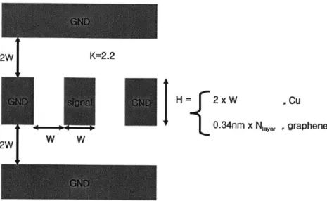
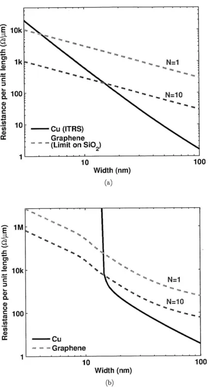
In this section, we compare the performance of graphene and Cu wires using a typical wire structure with adjacent ground signals and ground planes (Figure 2-8). The interlayer dielectric constant is r=2.2 and the aspect ratio is fixed at 2 for Cu wires. Figure 2-9 shows the resistance of graphene and Cu wires. When graphene is limited by the SiO2 substrate, graphene begins to outperform Cu below 14 nm wire
width for 10-layer graphene wires and below 4 nm wire width for monolayer graphene interconnects. As more layers of graphene are used, the width at which graphene begins to outperform Cu increases. However, these projections are based on the upper limit of graphene. ITRS projections also assume high quality Cu wires where scattering induced by line-edge roughness is limited. In Figure 2-9b, we assume more realistic values equivalent to those used in Section 2.1.3 and Section 2.2. Under these assumptions, line-edge roughness severely limits the Cu wires below 14 nm, resulting in the rapid rise in resistance. Both monolayer and 10-layer graphene wires show better performance than Cu wires below 14 nm.
2W K=2.2
H = 2 x W ,CU
1
1
0.34nm
x
Nay, graphene
2W W W
Figure 2-8: Cross section of interconnect and surrounding ground planes. The dielec-tric constant is K=2.2 and the aspect ratio is 2 for Cu wires. The estimated height H of the graphene wire is the product of the interlayer spacing 0.34 nm and the number of layers.
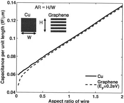
as the modeled parameters change. However, in general, this crossover is not expected to occur until around 10 nm which is consistent with [33]. In contrast to resistance values, the capacitance of the graphene wire is known to be significantly less than that of a Cu wire. Figure 2-10 shows the capacitance per unit length as a function wire width assuming the geometry outlined in Figure 2-8. The capacitance of the Cu wire is nearly constant across all wire widths because the geometry scales accordingly. Recall that the total capacitance of a graphene wire can be expressed as the series combination of the electrostatic capacitance and quantum capacitance. As the wire width decreases, the capacitance of the graphene wire slightly increases since we assume that the graphene wire has constant thickness in contrast to the Cu wire, which has a constant aspect ratio. The difference between a monolayer and 20-layer graphene wire is relatively small when W=100 nm. When W=100 nm, the capacitance of a 20-layer graphene wire is only 7.4 % higher than that of a monolayer graphene wire. This difference becomes 79.6 % when W=10 nm. Overall, if we use less than 10 layers, the capacitance of a graphene wire is 2x lower than that of a Cu wire.
E 10 k
1
1k
0)%N=1
100 N=10 10 -- Cu (ITRS) Graphene (Limit on SiO2 10 100 Width (nm) (a)~1M-14 10k -N=10 CL N=10 C 100-CDU --- Cu Graphene 10 100 Width (nm) (b)
Figure 2-9: Resistance per unit length. (a) Graphene is calculated as the limit on SiO2. Cu model assumes ITRS projection where
(pc,=0.95,Rer=0.45,LER=O,
H=2xW).
(b) zigzag graphene assumes EF=0.2eV, AD=1 puM, Pc=0.5. Cu model0.16
E 0.14- (constant AR)
LL
.N=60
0.12 - Graphene
%) 4. (metallic, EF=O.2eV)
=0.1
2 (constant height) c . 0.08 - N=10 C M N=5 0.06 - -CL 0.04- N=1 3 10 100 Width (nm)Figure 2-10: Capacitance of graphene and Cu wires. Cu wires assume a constant aspect ratio=2. Graphene wires are assumed to be zigzag with EF=0.2eV.
layers also increases the capacitance and energy dissipation. Figure 2-11 plots the wire capacitance at a fixed width of 10 nm. Generally, the quantum capacitance is much larger than the electrostatic capacitance and thus has very little effect on the overall capacitance especially for thicker graphene films. As the number of layers increase, the capacitance also increases. In contrast, the resistance shows a more pronounced decrease as the number of layers increase (Figure 2-12). If we assume a smooth edge with no scattering, roughly -16 layers is needed to match the resistance of a Cu wire. However, more than 60 layers is required when the wire is completely diffusive. Thus, fabricating multiple graphene layers with very little interlayer and line-edge scattering is necessary to have resistance values comparable to that of Cu wires.
Similarly, the combined effect of the wire resistance and capacitance is shown in Figure 2-13. Because the wire capacitance shows a rather weak dependence on the number of layers, the RC time constant shows a similar form as the wire resistance. Nonetheless, the small capacitance of graphene does lower the overall RC time
con-0.04
10 20 30 40 50
Number of layers
Figure 2-11: Wire capacitance as a function of number of graphene layers. Wire width is fixed at 10 nm. Cu wire assumes an aspect ratio of 2.
100k 10k 1k 100 Cu (ITRS) Graphene - (EF=0. 2eV =lgm)1 smooth edge (P SC=0) diffusive edge (P =1) Limit on SiO 10 20 30 40 50 Number of layers Figure 2-12: Wire is fixed at 10 nm.
resistance as a function of number of graphene layers. Wire width Cu wire assumes an aspect ratio of 2.
Cu (ITRS)
lou - - Graphene (EF=0.2eVXD=1pm) _E 1u -7 _0. smooth edge T(P
=0)
diffusive edge
% (P=1)
10n
Limit on SiO
2 10 20 30 40 50Number of layers
Figure 2-13: RC delay as a function of number of graphene layers. Wire width is fixed at 10 nm. Cu wire assumes an aspect ratio of 2.
stant and only ~ 8 layers is needed to match the RC time constant of a Cu wire when a smooth edge is assumed. When the wire is completely diffusive, more than 60 layers is still required to match the performance of Cu wires. When graphene approaches its limit on SiO2, only two layers of graphene is needed to match the RC time constant of Cu. This suggests that the graphene films needs to be of extremely high quality.
2.3.3
Interconnect Performance for Subthreshold Circuits
Enhancing the quality of the graphene wire and fabricating multilayer stacks is critical for lowering the delay of graphene wires. Overcoming these challenges may prove to be too difficult as no known solutions exist yet. One attractive alternative is to take advantage of the small capacitance of graphene wires. Chip makers will often produce two different silicon technologies depending on the system needs. For example, interconnect stacks are often optimized either for RC performance or wire density [75]. In high-performance applications, thick wires are used to optimize the

![Figure 2-5: Mobility of graphene wires vs. wire width. Data points are from [43] and lines represent calculated mobility.](https://thumb-eu.123doks.com/thumbv2/123doknet/14675061.557768/34.918.227.665.139.465/figure-mobility-graphene-wires-points-represent-calculated-mobility.webp)
![Figure 2-7: Sheet resistance of graphene and Cu. Data points are measured results from [55].](https://thumb-eu.123doks.com/thumbv2/123doknet/14675061.557768/38.918.232.654.147.443/figure-sheet-resistance-graphene-data-points-measured-results.webp)