Design and Fabrication of a MEMS-Array Pressure Sensor
System for Passive Underwater Navigation Inspired by the
Lateral Line
by
Stephen Ming-Chang Hou
M.Eng., Electrical Engineering and Computer Science Massachusetts Institute of Technology, 2004
S.B., Electrical Science and Engineering Massachusetts Institute of Technology, 2003
S.B., Physics
Massachusetts Institute of Technology, 2003
Submitted to the Department of Electrical Engineering and Computer Science in partial fulfillment of the requirements for the degree of
Electrical Engineer at the
MASSACHUSETTS INSTITUTE OF TECHNOLOGY June 2012
c
Massachusetts Institute of Technology 2012. All rights reserved.
Author . . . . Department of Electrical Engineering and Computer Science
March 14, 2012
Certified by . . . . Jeffrey H. Lang Professor of Electrical Engineering Thesis Supervisor
Accepted by . . . . Leslie A. Kolodziejski Chair, Department Committee on Graduate Theses
Design and Fabrication of a MEMS-Array Pressure Sensor System for Passive Underwater Navigation Inspired by the Lateral Line
by
Stephen Ming-Chang Hou
Submitted to the Department of Electrical Engineering and Computer Science on March 14, 2012, in partial fulfillment of the
requirements for the degree of Electrical Engineer
Abstract
An object within a fluid flow generates local pressure variations that are unique and char-acteristic to the object’s shape and size. For example, a three-dimensional object or a wall-like obstacle obstructs flow and creates sharp pressure gradients nearby. Similarly, un-steady flow contains vortical patterns with associated unique pressure signatures. Detection of obstacles, as well as identification of unsteady flow features, is required for autonomous undersea vehicle (AUV) navigation. An array of passive underwater pressure sensors, with their ability to “touch at a distance” with minimal power consumption, would be able to resolve the pressure signatures of obstacles in the near field and the wake of objects in the intermediate field. As an additional benefit, with proper design, pressure sensors can also be used to sample acoustic signals as well.
Fish already have a biological version of such a pressure sensor system, namely the lateral line organ, a spatially-distributed set of sensors over a fish’s body that allows the fish to monitor its hydrodynamic environment, influenced by the external disturbances. Through its ability to resolve the pressure signature of objects, the fish obtains “hydrodynamic pictures”.
Inspired by the fish lateral line, this thesis describes the development of a high-density array of microelectromechanical systems (MEMS) pressure sensors built in KOH-etched silicon and HF-etched Pyrex wafers. A novel strain-gauge resistor design is discussed, and standard CMOS/MEMS fabrication techniques were used to build sensors based on the strain-gauge resistors and thin silicon diphragms. Measurements of the diaphragm deflection and strain-gauge resistance changes in response to changes in applied external pressure confirm that the devices can be reliably calibrated for use as pressure sensors to enable passive navigation by AUVs. A set of sensors with millimeter-scale spacing, 2.1 to 2.5 µV/Pa sensitivity, sub-pascal pressure resolution, and −2000 Pa to 2000 Pa pressure range has been demonstrated. Finally, an integrated circuit for array processing and signal amplification and to be fabricated with the pressure sensors is proposed.
Thesis Supervisor: Jeffrey H. Lang Title: Professor of Electrical Engineering
Acknowledgments
This thesis would not have been possible without the efforts of many people. First, I would like to express gratitude to my advisor, Prof. Jeff Lang, for the opportunity to work under his mentorship throughout my graduate studies. His deep intuition and focus on important questions will always influence me. I thank the other faculty under whom I have worked on various projects over the years, Profs. Franz Hover, Marty Schmidt, Alex Slocum and Michael Triantafyllou, for their creative insights and guidance. Their boundless supply of energy, enthusiasm and knowledge make MIT such an incredible place to study.
I would like to thank the other members of the Underwater Sensors Group and the Precision Engineering Research Group. I am grateful to my officemate Dr. Vicente Fer-nandez, who worked on complementary aspects of our overall project, for our conversations and mutual encouragement. I am especially thankful to Drs. Hong Ma, Alexis Weber and James White for their many hours showing me the ropes in the lab when I first started, and generously providing many pieces of advice throughout, even when they were busy prepar-ing to graduate. Drs. Jian Li, Joachim Sihler and Xue’en Yang also extended invaluable tips on fabrication techniques.
I would like to thank other members of the MEMS community at MIT. In particular, I thank Prof. Joel Voldman for sharing his experience with HF etching. I would like to thank Kevin Nagy and Dr. Nikolay Zaborenko for their bonding recipes, and countless other fabrication laboratory users for sharing bits of advice, which has motivated me to contribute to our collective knowledge.
In the spirit of the collaborative nature of MIT, I thank Drs. Steve Bathurst, Jerry Chen, Ivan Nausieda and Vanessa Wood for sharing their laboratory equipment for experimenting with printable electronics.
I would like to express great appreciation for the MIT Microsystems Technology Lab-oratories (MTL), i.e. my second home, where my fabrication work was carried out. In particular, I am grateful to MTL staff members Bernard Alamariu, Bob Bicchieri, Kurt Broderick, Eric Lim, Kris Payer, Dave Terry, Paul Tierney, Tim Turner and Dennis Ward, who patiently trained me on each of the machines, maintained tools around the clock, answered my calls and e-mails when I needed help, and offered advice.
to Wayne Ryan and Steve Turschmann for building various equipment that my research required.
I would like to thank the National Science Foundation, the NOAA MIT Sea Grant College Program (project grant R/RT-2/RCM-17), the MIT-Singapore Alliance, the MIT Deshpande Center and the MIT Department of Electrical Engineering and Computer Sci-ence (EECS) for their funding of my research.
I would like to thank Sam Chang, Dr. Shahriar Khushrushahi, Adam Reynolds, Yasu Shirasaki and my family for taking the time to read my thesis and offer improvements, especially on short notice. However, any outstanding errors are mine alone.
Of course, I am grateful to those at MIT who have provided me with a life outside the lab. I will always remember my friends from the Graduate Student Council, the EECS Graduate Students Association, the Resources for Easing Friction and Stress and Ashdown House for inspiring a selfless sense of community and belonging. I also appreciate the EECS department, the Educational Studies Program and BLOSSOMS for the distinct privilege of teaching bright young people on behalf of MIT.
Finally, I would like to thank my family for their unwavering support and encourage-ment. I am indebted to my parents’ dedicated efforts in providing me the opportunities I’ve had throughout my life. Their eternal love and faith in me will be carried to future generations. I dedicate this thesis to them.
Contents
1 Introduction 21
1.1 The Fish Lateral Line and Biomimetics . . . 24
1.2 MEMS Pressure Sensors: A Broader Context . . . 27
1.3 Where This Work Fits In . . . 32
1.4 Project Summary . . . 35
1.5 Thesis Organization . . . 37
2 Device Design 39 2.1 Overview of Device Features . . . 40
2.2 Wafer-Level Design . . . 43 2.2.1 Air channels . . . 43 2.2.2 Round 1 . . . 44 2.2.3 Round 2 . . . 45 2.2.4 Round 3 . . . 48 2.2.5 Round 4 . . . 50 2.2.6 Round 5 . . . 50 2.3 Properties of Silicon . . . 52
2.3.1 Crystalline structure of silicon . . . 52
2.3.2 The elastic properties of silicon . . . 53
2.3.3 The elastic properties of thin silicon diaphragms . . . 55
2.4 Wheatstone Bridge Circuit . . . 57
2.5 Piezoresistive Pressure Sensors . . . 60
2.6 Mechanical Model of the Diaphragm . . . 64 7
2.6.1 Diaphragm assumptions . . . 64
2.6.2 Governing equations . . . 65
2.6.3 The nature of the deflection function . . . 67
2.6.4 Deflection as a function of pressure . . . 68
2.6.5 Strain as a function of pressure . . . 70
2.6.6 Stress as a function of pressure . . . 71
2.7 Strain-Gauge Resistors . . . 73
2.7.1 Relative change in resistance of an infinitesimally small resistor . . . 73
2.7.2 Simulating resistance change . . . 74
2.7.3 Strain-gauge resistor pattern . . . 78
2.8 Sensitivity . . . 80
2.9 Dynamics . . . 82
2.10 Summary of Expected Performance . . . 84
3 Fabrication 85 3.1 Overview of Fabrication of Round 4 Devices . . . 86
3.2 Variations on Fabrication for Rounds 1, 2, 3a and 3b . . . 90
3.3 Photolithography . . . 92
3.4 Potassium Hydroxide Etching of (100) Silicon . . . 95
3.4.1 Silicon nitride mask and silicon oxide etch stop . . . 96
3.4.2 Finding the crystalline plane . . . 98
3.4.3 Mechanical wafer protection . . . 99
3.5 Pyrex Etching . . . 102
3.5.1 Substrate material . . . 102
3.5.2 Process flow for etching Pyrex . . . 102
3.5.3 Process design for etching Pyrex . . . 107
3.5.4 Masking materials . . . 107
3.5.5 Pyrex etchants . . . 109
3.5.6 Importance of retaining photoresist on gold . . . 109
CONTENTS 9
3.7 Process Design . . . 113
3.7.1 Order of key steps . . . 113
3.7.2 Placement of insulating oxide growth step . . . 115
3.7.3 Open access to cavities . . . 115
3.7.4 Wet processing bonded wafers . . . 116
3.8 Mask Design . . . 117 3.8.1 List of masks . . . 117 3.8.2 Mask alignment . . . 117 4 Measurements 121 4.1 Photographs of Devices . . . 122 4.2 Instrumentation . . . 126 4.2.1 Manometer . . . 126 4.2.2 Zygo profilometer . . . 128
4.2.3 Off-wafer differential amplifiers . . . 129
4.2.4 Tech-Etch cable . . . 131 4.2.5 Water-level probe . . . 132 4.3 Deflection . . . 134 4.4 Drifting Signals . . . 141 4.4.1 Experimental set up . . . 141 4.4.2 Dummy bridge . . . 142 4.4.3 E&M interference . . . 142 4.4.4 Fluctuating pressure . . . 143
4.4.5 Unstable contact resistance . . . 144
4.4.6 Stabilizing the contact resistance . . . 144
4.4.7 Gold on chromium . . . 147
4.5 External Bridge Measurements from Isolated Sensors . . . 148
4.6 Underwater Testing . . . 159
4.6.1 Out-of-water tests . . . 160
4.7 Summary of Measurements . . . 163
5 Concluding Remarks 165 5.1 Summary . . . 166
5.2 Contributions and Conclusions . . . 168
5.3 Future Work . . . 170
5.3.1 Further testing of Round 4 devices . . . 170
5.3.2 Improved strain-gauge design . . . 170
5.3.3 Integrated amplifier and array read-out circuitry . . . 172
5.3.4 Flexible substrates . . . 177
A Chemical Formulas 181 B Standard Operating Procedures 183 B.1 Mask-Making . . . 184 B.2 TRL Photolithography . . . 185 B.2.1 Double-sided PR . . . 187 B.2.2 With paint . . . 187 B.3 KOH Etching . . . 188 B.4 Post-KOH Clean . . . 190 B.5 Hot Phosphoric . . . 192
B.5.1 ICL hot phosphoric . . . 192
B.5.2 TRL acid hood . . . 192
B.6 EV501 and Anodic Bonding . . . 194
C Process Flows 197 C.1 Standard Photolithography . . . 198
C.2 Finding the Crystalline Plane for (100) Silicon . . . 199
C.3 Strain-Gauge Silicon Sensors Without Transistors . . . 200
CONTENTS 11
D Masks 209
E Apparatus 223
List of Figures
1-1 Finnegan the RoboTurtle. . . 22
1-2 Fish behaviors mediated by the lateral line. . . 23
1-3 Typical locations for the lateral lines in fish. . . 25
1-4 Cross-section and plan view of a typical bulk micromachined piezoresistive pressure sensor. . . 29
1-5 Cross-section of a typical silicon/Pyrex capacitive pressure sensor. . . 30
1-6 The Druck resonant pressure sensor. . . 30
1-7 Principal mechanical properties of a sensor as functions of diaphragm thick-ness and length. . . 31
1-8 Four potential applications of the biomimetic pressure sensor array system. 33 2-1 Diagram of pressure-sensor array with basic structure depicted. . . 40
2-2 Side view of a single sensor. . . 42
2-3 Schematic of air channels for underwater sensors. . . 44
2-4 Overlay of Round 1 devices. . . 46
2-5 Layout of resistors from Rounds 2 and 3. . . 47
2-6 Overlay of Round 3b devices. . . 49
2-7 Overlay of Round 4 devices. . . 51
2-8 Crystal planes and major directions. . . 52
2-9 Crystal orientation in (100) silicon wafers. . . 53
2-10 The Wheatstone bridge circuit. . . 57 13
2-11 Four resistors along a h110i direction at the centers of the four edges of the
surface of a square diaphragm. . . 61
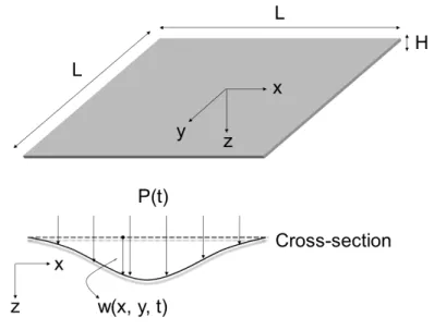
2-12 A square diaphragm of length L and thickness H. . . 65
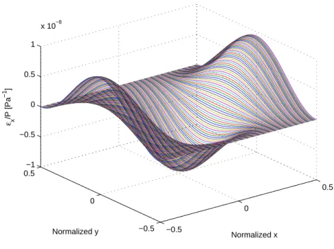
2-13 The strain of the top surface of the diaphragm in the x direction (ǫx) as a function of normalized positions. . . 75
2-14 The local optimal resistor lengthwise orientation for maximizing resistance change. . . 76
2-15 The sign of the resistance change when a local resistor is placed in the optimal direction. . . 77
2-16 The design of four strain-gauge resistors on a square diaphragm. . . 79
3-1 Standard photolithography. . . 93
3-2 Mask-making process. . . 94
3-3 Examples of KOH-etching (100) silicon. . . 97
3-4 Side view of KOH wafer holder. . . 100
3-5 Two-sided alignment mechanism. . . 118
3-6 Mask alignment marks. . . 119
4-1 Device from Round 1 (silicon diaphragm without strain-gauge resistors). . . 122
4-2 An entire wafer from Round 2 (strain-gauge resistors on dummy nitride wafer).123 4-3 An entire wafer from Round 3 (isolated strain-gauge sensors). . . 124
4-4 An entire wafer from Round 4 (interconnected sensors). . . 125
4-5 Manometer used to control the pressure in the cavities of devices from Rounds 1 and 3. . . 127
4-6 Photograph of the Zygo profilometer. . . 128
4-7 Circuit diagram of off-wafer differential amplifier. . . 129
4-8 Static and frequency responses of off-wafer differential amplifiers. . . 130
4-9 Photograph of the head of the Tech-Etch cable. . . 131
4-10 Photograph of the water-level probe (sideways). . . 132
LIST OF FIGURES 15 4-12 Profiles of a 2828 µm diaphragm at a pressure of −1500 Pa. . . 134 4-13 Profiles of a 2828 µm diaphragm at a pressure of +1500 Pa. . . 135 4-14 The deflection of the center of the diaphragm at various pressures for two
different sizes. . . 139 4-15 The deflection of the center of the diaphragm at various pressures for a 4000
µm diaphragm. . . 140 4-16 Experimental set up for testing one strain-gauge resistor. . . 142 4-17 The amplified output of an external bridge testing a single resistor on a 4000
µm diaphragm over an 80-second period. . . 143 4-18 Contact resistance stabilized by regular epoxy and microscope probe needle
tips. . . 146 4-19 Contact resistance stabilized by WEST SYSTEM epoxy and microscopeR
probe needle tips. . . 146 4-20 Contact resistance stabilized by both types of mechanical epoxies and
micro-scope probe needle tips. . . 147 4-21 The output of an external bridge from a 4000 µm diaphragm undergoing
±1600 Pa changes. . . 149 4-22 The output of an external bridge from a 4000 µm diaphragm undergoing
±200 Pa changes. . . 150 4-23 The output of an external bridge from a 4000 µm diaphragm undergoing a
200 Pa step. . . 151 4-24 External bridge voltage vs. pressure for various resistors from a 4000 µm
diaphragm. . . 152 4-25 External bridge voltage vs. pressure for various resistors from a 2828 µm
diaphragm. . . 153 4-26 External bridge voltage vs. pressure for various resistors from another 2828
µm diaphragm. . . 154 4-27 External bridge voltage vs. pressure for various resistors from a 2000 µm
4-28 External bridge voltage vs. pressure for various resistors from another 2000
µm diaphragm. . . 156
4-29 Photograph of a mounted wafer with pressure sensors that can be used un-derwater (Round 4). . . 159
4-30 Sample trace of two pressure sensors 2 cm apart (Round 4) activated by air gun swiped across wafer. . . 160
4-31 Bucket set up. . . 161
4-32 Resonant bucket waves. . . 162
5-1 Interconnect wiring of an array of pressure-sensing cells. . . 172
5-2 Schematic of the integrated transistor amplifier and array read-out circuitry for a 2 × 2 array. . . 173
5-3 Layout of one cell of the integrated transistor amplifier and array read-out circuit. . . 174
5-4 Side view of the strain-gauge pressure sensor with integrated transistor am-plifier and array read-out circuitry. . . 175
5-5 Diagram and photograph of the elastomer-based pressure sensors described in [96]. . . 178
5-6 Diagram of the three-terminal squitch described in [64]. . . 179
D-1 Mask P (Rounds 1 and 3a). . . 210
D-2 Mask N (Rounds 1 and 3a). . . 211
D-3 Mask M (Rounds 1 and 3a). . . 212
D-4 Mask D (Round 1). . . 213
D-5 Mask R (Rounds 2, 3a and 3b). . . 214
D-6 Mask D (Round 3a). . . 215
D-7 Mask P (Round 3b). . . 216
D-8 Mask O (Round 3b). . . 217
D-9 Mask D (Round 3b). . . 218
LIST OF FIGURES 17
D-11 Mask O (Round 4). . . 220
D-12 Mask D (Round 4). . . 221
D-13 Mask R (Round 4). . . 222
E-1 KOH wafer holder: bottom view of bottom piece. . . 224
E-2 KOH wafer holder: bottom view of top piece. . . 225
E-3 KOH wafer holder: top view of top piece. . . 226
List of Tables
2.1 Piezoresistive coefficients along a h110i direction for both types of doped silicon. 60 2.2 Expected performance parameters for strain-gauge pressure sensors of various
diaphragm lengths L. . . 84
3.1 Variations on fabrication for Rounds 1, 2, 3a, 3b and 4. . . 91
3.2 Diagram of cross-sectional trench profiles from different types of etch methods. 95 3.3 Process flow for etching Pyrex wafers. . . 104
4.1 Slopes c1/P for various diaphragm lengths L. . . 136
4.2 Experimental values of slopes of best-fit lines for amplified voltage vs. pres-sure for strain-gauge resistors on various diaphragms from Round 3b. . . 157
4.3 Theoretical values of slopes of best-fit lines for amplified voltage vs. pressure for strain-gauge resistors on various diaphragms from Round 3b. . . 157
A.1 Chemical formulas and full names. . . 181
B.1 Recipe for bonding silicon and Pyrex. . . 195
C.1 Process flow for standard single-sided photolithography. . . 198
C.2 Process flow for standard double-sided photolithography. . . 198
C.3 Process flow for finding the crystalline plane for (100) silicon. . . 199
C.4 Process flow for Pyrex wafers for strain-gauge silicon sensors without tran-sistors. . . 201 C.5 Process flow for SOI wafers for strain-gauge silicon sensors without transistors.201
C.6 Process flow for SOI wafers for strain-gauge silicon sensors without transistors (cont.). . . . 202 C.7 Remainder of process flow for strain-gauge silicon sensors without transistors. 203 C.8 Process flow for Pyrex wafers for strain-gauge silicon sensors with transistors. 205 C.9 Process flow for SOI wafers for strain-gauge silicon sensors with transistors. 206 C.10 Process flow for SOI wafers for strain-gauge silicon sensors with transistors
(cont.). . . . 207 C.11 Process flow for SOI wafers for strain-gauge silicon sensors with transistors
(conc.). . . . 207 C.12 Remainder of process flow for strain-gauge silicon sensors with transistors. . 208 D.1 List of masks used for each round of devices. . . 209
Chapter 1
Introduction
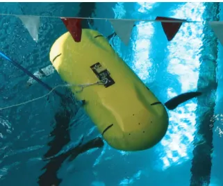
Many methods of sensing have been used by undersea vehicles to obtain three-dimensional mappings of the surrounding ocean floor, walls and other objects. Such maps aid vehicles in navigating through unfamiliar territory, avoiding collisions with moving objects, and surveilling the environment. The most common methods–sonar, radar and optical sensing– require active transceivers and thus use significant amounts of power. For small autonomous undersea vehicles (AUVs), such as the one depicted in Figure 1-1, space and energy are precious as energy must be stored on board and should be reserved for motion, especially propulsion. Additionally, in cluttered environments or poor visibility conditions such as murky surf zones, topological mapping by sonar or optical sensing becomes difficult as signal to noise is drastically reduced and the process depends strongly on the acoustic environment (e.g., multipath). Furthermore, the required equipment may occupy much of the payload space of the vehicle. Therefore, a simple compact passive sensing system that does not require high power would be ideal for such vehicles.
One domain where passive sensing can be achieved is fluid pressure. An object within a fluid flow generates local pressure variations that are unique and characteristic to the object’s shape and size. For example, a three-dimensional object or a wall-like obstacle obstructs flow and creates sharp pressure gradients nearby. Similarly, unsteady flow contains vortical patterns with associated unique pressure signatures. Detection of obstacles, as well as identification of unsteady flow features, is required for vehicle navigation. An array
Figure 1-1: Finnegan the RoboTurtle, an MIT-developed biomimetic autonomous undersea vehicle (AUV), navigating in a swimming pool.
of passive underwater pressure sensors, with their ability to “touch at a distance” with minimal power consumption, would be able to resolve the pressure signatures of obstacles in the near field and the wake of objects in the intermediate field. As an additional benefit, with proper design, pressure sensors can also be used to sample acoustic signals as well.
Fish already have a biological version of such a pressure sensor system, namely the lateral line organ, and this thesis is inspired by their approach. The blind Mexican cavefish, Astyanax fasciatus, can form full real-time three-dimensional maps of its surroundings to move in unfamiliar environments at high speeds without collisions [59, 89]. Unlike the electrolocation sense found in some species of fish, A. fasciatus accomplishes this surprising feat without the use of electric fields, and instead relies primarily on its lateral line organ. While all fish have this organ, not all use it to the extent that the blind cavefish does [59]. The lateral line is a spatially-distributed set of sensors over a fish’s body that allows the fish to monitor its hydrodynamic environment, influenced by external disturbances. Through its ability to resolve pressure signatures of objects, the fish obtains “hydrodynamic pictures”, enabling the lateral line to act like a “touch at a distance” device.
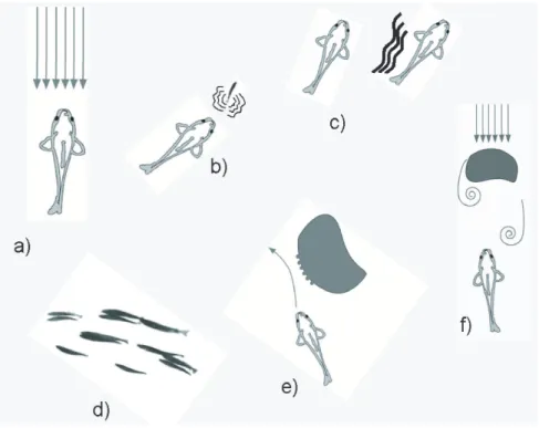
Many other lateral-line-mediated behaviors in fish have been identified by biologists [67, 89], including (a) rheotaxis, or orienting themselves to currents and holding stationary in
23 strong currents; (b) detecting, localizing and tracking prey by their wake; (c) communicating with other fish; (d) matching their own swimming speed and direction to that of their neighbors while performing tight and rapid schooling maneuvers; (e) recognizing nearby physical objects; and (f) swimming efficiently. These behaviors are depicted in Figure 1-2. In the world of AUVs, there is currently no pressure sensing equivalent to the lateral line organ. However, with its diverse capabilities in nature, the lateral line has advantageous features to offer AUV navigation technology.
Figure 1-2: Fish behaviors mediated by the lateral line. (a) rheotaxis, (b) prey detection and tracking, (c) communication, (d) schooling, (e) recognizing objects, (f) swimming efficiently.
This thesis is part of ongoing work toward the development of high-density arrays of microelectromechanical systems (MEMS) pressure sensors to enable passive navigation by AUVs. Inspired by the fish lateral line, we are developing inexpensive, low-power sensors that passively measure static and dynamic pressure fields around an AUV with sufficient spatial and time resolution to detect and map objects generating the hydrodynamic distur-bance. Related projects within our research group include the development of processing
schemes that use the sensors pressure information to detect, identify and classify objects in the flow environment for AUV navigation and control [32, 30, 31]. Combining the sensors and processing software not only emulate but also extend the capabilities of the lateral line in fish. The sensor arrays will be capable of detecting field flow patterns and near-and far-body obstacles near-and vehicles, as well as mapping near-body objects. This would be a unique capability for navigation in shallow water and/or cluttered environments, for use with multiple AUVs, and for flow control in conventional and biomimetic1vehicles. Another application of our sensor is to determine the pressure distribution on the propellors, sails and hulls of sea vehicles for optimizing design and improving performance. We envision that at the end of these projects, these sensors will emerge as a standard, low-cost system available in most AUVs.
While this thesis focused on implementing a sensor system using rigid and flat silicon, we eventually want to build a system using flexible or custom-shaped soft polymer materials, which would enable users to place a sensor system flush against curved surfaces, such as fins and hulls. Furthermore, silicon is brittle whereas polymers can be quite robust. Polymers could be a better choice for the mechanically rough undersea environment. With these future directions in mind, we designed a silicon-based sensor with technical approaches that can be easily transferred to polymer-based technology. For example, while piezoresistive sensors are widely used to build silicon sensors, this technique does not work in polymers. Instead, we chose to develop a strain-gauge sensor. Based on this concept, members of our research group have explored fabricating underwater pressure sensor arrays using conductive polymers [96].
1.1
The Fish Lateral Line and Biomimetics
The basic sensory unit of the fish lateral line organ is the neuromast, which is a collection of drag-based flow velocity sensors. Neuromasts are used in two manners. First, they are distributed on the surface of the fish and protrude directly into the open water. In this
1Biomimetics is the study of biological systems as models for the design of engineered materials and machines.
1.1. THE FISH LATERAL LINE AND BIOMIMETICS 25
Figure 1-3: Typical locations for the lateral lines in fish (red). Reproduced from [34].
arrangement, the neuromasts are directly stimulated by the local fluid velocity to sense flow. As shown in Figure 1-3, the specific distribution of neuromasts varies widely from species to species. Second, the neuromasts are enclosed in canals with pores that open to the outside flow periodically [34]. These canals have been described as an array of pressure gradient sensors [20], where a pressure difference between adjacent pores drives fluid motion in the canal, and thereby stimulates the neuromasts. Studies that selectively deactivated the canals found that the mapping abilities of the lateral line appear to be predominantly accomplished by its canal system [59]. By measuring the pressure gradient as a function of location along the fish’s body and time, the fish is able to locate and identify nearby objects as well as determine their shapes and velocities.
While the lateral line organ cannot be identically implemented with standard fabrication technologies, the capabilities similar to that of the lateral line would greatly benefit AUVs. In particular, the ability to locate and obtain information about nearby obstructions is increasingly important as AUVs are finding applications in cluttered environments and surf zones. Also, the ability for flow mapping and identifying vortical structures allows the possibility for optimizing control and navigation in unsteady environments. In addition to
these capabilities, a distributed pressure sensor system would be completely passive and consequently require little power. Compared to active systems like sonar, the primary disadvantage of a pressure sensor system would be its limited range, or the maximum distance of detected objects.
A number of researchers have experimentally and numerically studied the fish’s lateral line and its ability to identify objects and flow structures. In investigating the blind fish’s object sensing skills, [89] constructed a model neuromast and demonstrated the neuromast’s ability to locate plates and thin beams at a distance of 2 mm. [40, 41] measured the dynamic pressure distributions generated on the body of a model fish when gliding alongside and into a wall at similar millimeter-scale distances. [87] showed that goldfish use their lateral line to detect and discriminate the size, velocity and shape of passing rods in still water. Numerical experiments by [79] demonstrated that an array of pressure sensors could track the position and circulation in a channel. While free stream flows are more complex and unpredictable in open water than single vortices are, [79] established that an array of pressure sensors is a viable way to identify and track vortices. The question remains how well a simple pressure sensor array is able to distinguish between moving objects of different shapes and sizes.
Our group has used commercial pressure sensors separated on the order of 10 millimeters to record pressure signals resulting from flow around both still and moving objects. Using principal component analysis (PCA) and Kalman filtering on the recorded signals, we could discriminate between various cylindrical objects with round and square cross-sections of sizes on the order of several centimeters. Similarly, we could track motion up to half a meter per second using commercial pressure sensors separated on the order of several millimeters apart. We found that a classification error rate of under 2% can be achieved with a 2 kPa range, 10 Pa resolution, and 60 Hz data acquisition rate [30, 31, 23]. The pressure sensor spacing would need to be on the order of millimeters in order to capture the relevant features in a single instance, which would be necessary under non-uniform conditions found outside laboratory conditions.
1.2. MEMS PRESSURE SENSORS: A BROADER CONTEXT 27
1.2
MEMS Pressure Sensors: A Broader Context
Microelectromechanical systems (MEMS)2 are micro-scale devices that enable the operation of complex systems by converting physical stimuli from the mechanical, thermal, chemical and optical domains to the electrical domain. MEMS engineers engage technologies across a wide set of scientific disciplines, including physics, chemistry, material science, integrated circuit (IC) fabrication and manufacturing. Due to its origins from the IC industry, much of MEMS technology is based on silicon, the substrate material used for the vast majority of commercial electronics. However, there is ongoing research in other materials as well, such as plastics and ceramics, for their lower costs and biocompatibility for medical applications. As a result of its interdisciplinary nature, MEMS technology has found use in many industries, especially automotive, medical and aerospace. A device class where MEMS have thrived is sensing. For example, early crash sensors for airbag safety systems were merely mechanical switches. Today, airbag systems use MEMS sensors that not only measure acceleration, but also provide self-diagnostics and integration with other sensors in the vehicle. Other types of MEMS sensors currently undergoing rapid research progress include flow sensing for biomedical applications [3], microphones for portable devices [72], and accelerometers for touch screens and gaming [35, 69].
After accelerators, pressure sensors are the most commercially successful class of MEMS sensors. These devices employ a broad range of techniques to convert mechanical pressure into electrical signals, such as piezoresistive, capacitive, resonant, and strain-gauge resistive sensing. Furthermore, the list of applications of pressure sensors has also grown tremen-dously over the past three decades. As a result, pressure sensing has developed into a market where highly specialized devices can be found for specific needs. The fundamental specification of a pressure sensor is its operating pressure range. Other obvious parame-ters, such as physical dimensions, pressure resolution, reliability, lifespan, environmental compatibility and cost are also important, but there are more subtle considerations as well.
2Microelectromechanical systems is the term most commonly used in the United States. In Europe, the technology is generally known as microsystems technology (MST), whereas in Japan, the term micromachines is used in English-language publications. This thesis follows the U.S. convention.
The effects of temperature, long-term drift, hysteresis, linearity, and the dynamic response all influence the design and fabrication of a custom-made pressure sensor.
A popular design feature of pressure sensors is a micromachined flexible diaphragm. Depending on the application, such diaphragms range from tens to thousands of microns in width and from a few to hundreds of microns in thickness. Various types of diaphragm-based pressure sensors, such as piezoresistive, capacitive, resonator, and strain-gauge resistive sensors, are discussed in the remainder of this section. While the ultimate goal of the project is to implement pressure sensors in a soft or moldable material, we first tested sensor designs in silicon with technology that would also work with polymers.
Diaphragm-based pressure sensors rely on mechanical deformation of the diaphragm to alter the electrical properties of a sensing component on the diaphragm. Piezoresistive and strain-gauge resistive pressure sensors detect changes to resistance. Specifically, the resistance of a resistor with length l, cross-sectional area A and resistivity ρ is R = ρAl. Thus, there are two categories by which the resistance can change in response to strain: changes to the geometry (l or A) or changes to the conductive properties (ρ) of the resistor. The predominant cause of resistance change depends on the material. In metals, shape deformation, and thus changes to l and A, are the primary source of resistance change, leading to strain gauges. In silicon, ρ is affected by stress, and thus by strain, causing changes to R. This effect is called piezoresistivity, and electrical elements of this type are called piezoresistors.
Piezoresistive pressure sensors have resistors implanted on the diaphragm. When a pressure difference between the two faces of the diaphragm deforms the diaphragm, the strain is translated into a change in resistance. An example of a piezoresistive pressure sensor is shown in Figure 1-4. As will be discussed later in Section 2.5, the four resistors are located at the centers of the edges of the square diaphragm and are oriented in the same direction. One common application of piezoresistive pressure sensors is in the automotive industry, such as measuring diesel injection pressure and controlling exhaust gas recirculation systems. The major drawback to this technology is that the diaphragm is restricted to materials that have strong piezoresistive properties.
1.2. MEMS PRESSURE SENSORS: A BROADER CONTEXT 29
Figure 1-4: Cross-section and plan view of a typical bulk micromachined piezoresistive pressure sensor. Reproduced from [3].
A capacitor with one electrode attached to the flexible diaphragm can also sense pres-sure via changes in its capacitance. An example of a capacitive prespres-sure sensor is shown in Figure 1-5. Typical advantages of capacitive sensors include high sensitivity, low power consumption, and low temperature dependence. Also, capacitive sensors have been demon-strated in non-silicon materials, such as quartz and polymers [3, 60]. Unfortunately, de-pending on the specifics of the geometry of the devices and pressure range, there may be issues with hysteresis and static friction, or stiction. Furthermore, capacitive sensors tend to have nonlinear outputs and require complex electronics. To counter these problems, some implementations, such as intravascular blood pressure measurement and intracranial pressure [3], use multiple sensors to obtain a single pressure measurement. Since our ap-plications require an array of sensors, where each sensor produces a reliable local reading, capacitive sensing is not a suitable option.
Resonant pressure sensors rely on a resonating mechanical structure to detect diaphragm deformation. One of the earliest such sensors, commercialized by Druck, is shown in Fig-ure 1-6. High-performance resonant pressFig-ure sensors are particularly useful for high-pressFig-ure applications in the oil and gas industry, where accurate pressure measurement is essential [3]. Although the performance specifications can be quite impressive, the most attractive mate-rials for resonant sensors, such as quartz, are incompatible with integrated circuits, which
Figure 1-5: Cross-section of a typical silicon/Pyrex capacitive pressure sensor. Reproduced from [3].
is necessary for efficient addressing by an array of sensors. Other resonant pressure sen-sors measure the changes in electromagnetic resonant structures, such as inductor-capacitor (LC) cavities for tuning wireless electronics [46]. The concept is also used in medical engi-neering: CardioMEMS is developing devices that are passive LC resonator circuits and can be implanted in the patients heart chambers or into the pulmonary artery [18].
Figure 1-6: The Druck resonant pressure sensor. Reproduced from [3].
Finally, we consider the sensitivity and possible applications of diaphragm-based re-sistive strain-gauge sensors. Figure 1-7 shows the maximum deflection, maximum stress, maximum strain and lowest natural frequency of a square silicon diaphragm as functions
1.2. MEMS PRESSURE SENSORS: A BROADER CONTEXT 31
Figure 1-7: Principal mechanical properties of a sensor as functions of diaphragm thickness and length. Values are given for a pressure difference of 10 Pa. The nominal design is shown with circles.
of the primary geometric parameters of diaphragm: side length and thickness. Here, we assume that the diaphragm acts as a homogeneous plate with stiff boundaries at the edges that experiences a nominal gauge pressure of 10 Pa, the stagnation pressure associated with a flow of 14 cm/s. The deflection, stress and strain vary approximately linearly with pres-sure, and can therefore be scaled as needed. Indicated on each contour plot is the nominal design of a square diaphragm with a diameter of 2 mm and a thickness of 20 µm. The graphs confirm the strong variation in sensor properties with geometry. As expected, stiffness of the membrane increases dramatically with thickness, and inversely with diameter.
The stress and strain sub-plots show the maximum values, which occur at the center of the edges of the diaphragm, i.e. at the fours points halfway between adjacent corners of the diaphragm. If the ultimate strength of silicon is conservatively estimated to be
300 MPa, the nominal design is safely stressed for pressures approximately four orders of magnitude larger than the 10 Pa considered here, or 100 kPa. This compares favorably with commercial hydrophones available today, which have a typical overpressure in the range of 200 dB relative to 1 µPa, or 10 kPa. Furthermore, the fundamental natural frequency of the nominal pressure-sensing diaphragm is quite high, in the range of tens or hundreds of kilohertz. This frequency vastly exceeds the frequencies generated by near-field and mid-field pressure disturbances, which are on the order of tens of hertz for many natural and man-made structures, thus avoiding resonance. Acoustic transducers in use today, however, do exceed 1 MHz, namely in Doppler velocimetry loggers (e.g., RD Instruments Workhorse Navigator) and acoustic imaging systems (e.g., DIDSON). For positioning systems, lower frequencies in the neighborhood of 10–30 kHz are common for large-scale, multi-kilometer systems, whereas frequencies of 300 kHz have been used on scales of several hundred meters. Whales and dolphins communicate at frequencies up to 100 kHz. Hence, in addition to pressure sensing, a diaphragm-based sensor will also be capable of operating as a passive acoustic detector for the lower end of frequencies relevant in underwater acoustics.
1.3
Where This Work Fits In
This thesis demonstrates the design, fabrication and testing of MEMS strain-gauge silicon pressure sensor arrays inspired by the fish lateral line to enable passive navigation by AUVs. Figure 1-8 illustrates some of these applications, as well as related tasks that would be enabled by such a system of pressure sensors.
These sensing capabilities are becoming possible with the development of MEMS tech-nology to fabricate arrays containing hundreds or even thousands of pressure sensors. The sensors, each around 2 mm in length, can be arranged over a flat or curved surface in various configurations, such as a single line, a patch consisting of several parallel lines, or specialized forms to fit the hull shape of a vehicle or its fins. The sensors can be packaged closely together at distances of a few millimeters apart to be able to resolve pressure and flow features near the array spacing, which in turn can be used to identify the overall flow features.
1.3. WHERE THIS WORK FITS IN 33
Figure 1-8: Four potential applications of the biomimetic pressure sensor array system.
Both self-propelled vehicles and obstacles standing within a smooth or turbulent current generate flow disturbances. The near-field of this hydrodynamic disturbance extends typ-ically about one body length around the generating object and is characterized by strong pressure and velocity variations. Such near-body pressure variations are referred to as “pseudo-sound” and can be detected by a sensor which is close to the obstacle. If the disturbance is unsteady and its frequency is sufficiently high, the disturbances generates acoustical waves that create a far-field disturbance, which is detectable at hundreds or thousands of body lengths away, depending on the frequency. In addition, a hydrodynamic wake is shed by the body and is detectable directly downstream from the generating body as pressure and velocity fluctuations in the near and intermediate field, up to hundreds of meters away from the source. The sensors we developed are appropriate to all three of these regimes: pseudo-sound, high-frequency sound, and wakes, although we focused primarily on applications for pseudo-sound and wake flows. For some standard objects, hydrodynamic signatures and flow patterns are codified, so that the sensor system could potentially
au-tomatically detect objects and flow patterns. Our pressure sensor arrays can thus provide the following capabilities to AUVs:
1. Measure the distance to the near-field objects, obstacles and other vehicles. 2. Determine the location, speed, direction and size of moving vehicles and objects. 3. Form accurate topological maps of nearby objects through reconstruction of their
shapes from predetermined pressure hydrodynamic signatures.
4. Assist maneuvering in cluttered environments in the presence of turbidity and turbu-lence, and operations in the dark.
5. Assist in the coordination of multiple robots. Each robot vehicle will be provided at low power with effective images of the location and orientation of the near-by vehicles. 6. Identify flow patterns in the surrounding flow to optimize fin and propulsor perfor-mance. This flow information can also be used for energy extraction in biomimetic vehicles.
Other sensing technologies, such as sonar or radar, also use arrays sometimes, but these are limited to a few dozen in number and are centimeters or meters apart. The concept de-scribed in this thesis can be scaled to an array of several hundred of sensors, each millimeters apart.
This project is of interest not only to undersea researchers but also to the MEMS com-munity as well. Currently, much of MEMS sensor development is focused on designing single, extremely sensitive sensors for use in applications such as microphones [72]. Fur-thermore, research in sensor arrays tends to be motivated by tactile applications [78]. From the materials science perspective, undersea navigation provides motivation for MEMS re-search in flexible, non-silicon substrates. Finally, by successfully demonstrating an array of pressure sensors for undersea object identification, we hope the project will inspire further work in integrating MEMS with macro-scale systems for high-precision applications.
1.4. PROJECT SUMMARY 35
1.4
Project Summary
A MEMS pressure sensor system based on strain gauges bonded to silicon diaphragms was fabricated and tested. The system consists of a set of sensor cells spaced a few millimeters apart fabricated on etched silicon and Pyrex wafers. Silicon and Pyrex are well-understood MEMS substrates that provide a foundation for evaluating the feasibility of transferring our pressure sensor design to polymer substrates. The sensing element on each cell is a set of strain-gauge resistors mounted on a flexible 2-mm wide square diaphragm, which is a thin 20-µm layer of silicon attached at the edges to a square silicon cavity. The physical and electrical dimensions of the sensor components were chosen to satisfy the sensitivity and density specifications of the underwater environment. Finally, the sensors are attached to an array read-out system with sufficient voltage and time resolution to enable data output to a computer for further signal processing.
Several challenges were encountered in this project: read-out of an array of data, elec-tronics for signal-to-noise enhancement, mechanical robustness, the equilibration of the back pressure, dynamics and noise, and compatibility with polymers.
In order to develop a fully functional system ready for open water sensing and naviga-tion, we modularly tested individual aspects of the sensor system under highly controlled environments. However, all tests required the ability to read the array data. Thus, the ability to collect the outputs from the sensor array accurately and at a high data rate (kHz range) was of highest priority. As a first-pass solution, we have a pair of wires coming out of each sensor cell to a standard wire bundle that is fed into a computer. While this is acceptable for a small number of cells (fewer than 50), it is not easily scalable to hundreds or thousands of cells. One scalable solution is inspired by magnetic core memory: with transistor circuits connected to each sensor cell, signals address a particular column of cells, and the output signals from the entire column is returned. This reduces the output wiring to only a few fixed wires. However, while these electronics are conceptually simple, which is critical for moving the sensor design to soft substrates, reliable fabrication and calibration are significant challenges.
Since the undersea environment can be physically and chemically harsh, we designed the sensor system to be robust against possible damages. The design includes safety mechanisms that ensure that the loss of one cell will not affect the operation of the others. Of course, there are trade-offs between simplicity and robustness. We chose and fabricated a reasonable design that allowed us to test the system under controlled environments. In the future, we plan to develop a system that is able to handle more realistic situations but would require more complex electronics or layers of fabrication steps.
Another challenge is the equilibration of back pressure, which is pressure applied to the back-side of the diaphragms from within the sensor cavity. To reliably map flow velocities in the ocean, we are interested in detecting small-scale pressure fluctuations on the order of a few pascals. However, large-scale homogeneous pressure changes, such as those experienced when the entire system moves up or down relative to sea level would overwhelm any relevant signal.3 Furthermore, the sensors are physically limited in their dynamic range. Diaphragm-based sensors with sensitivity in the pascal range are not able to withstand pressures on the order of 105 Pa without physically breaking or leading to permanent damage. To design a robust sensor with good signal-to-noise, we remove the large-scale DC component of pressure change via a common back pressure. We designed fluidic channels that enable fast equilibration of the the back pressure so that our sensors are only detecting spatially varying pressure gradients.
This thesis describes the design, fabrication and static testing of individual MEMS strain-gauge silicon pressure sensors with amplification circuitry off-wafer. The results demonstrate that the proposed technology is feasible for the underwater object detection application described earlier. Remaining issues, including integrated amplifying and array-processing circuitry, dynamic responses, and full array testing underwater are left as future work.
1.5. THESIS ORGANIZATION 37
1.5
Thesis Organization
This chapter, Chapter 1, explains the motivation, background and objectives of the the-sis. Chapter 2 describes the design of the strain-gauge pressure sensor system. Chapter 3 explains the fabrication design of the device, including wafer etching, photolithography, pro-cess flow design and mask design. Chapter 4 contains the device measurements. Chapter 5 summarizes the work presented, conclusions drawn from the project, and suggestions for future directions.
There are several appendices that provide more detailed information relevant to the main text. Appendix A lists chemical formulas for common names and abbreviations used in this thesis. Appendix B contains standard operating procedures during fabrication. Appendix C contains full device process flows. Appendix D shows the masks used during fabrication. Appendix E contains technical diagrams of the various apparatus used in fabrication and measurement. Appendix F contains the MATLAB codes used for design analysis.
Chapter 2
Device Design
This chapter discusses the design of the strain-gauge pressure sensor system. Section 2.1 provides an overview of the device features. Section 2.2 describes the wafer-level features of the various pressure sensor systems fabricated. Section 2.3 describes the properties of silicon relevant for modeling device behavior and designing the fabrication process. Section 2.4 calculates the change in the output voltage of a Wheatstone bridge resulting from small changes in the sense resistances. Section 2.5 discusses a well-known pressure sensor based on piezoresistive properties of silicon, which provides a benchmark against which the strain-gauge pressure sensor is compared. Section 2.6 describes Kirchhoff-Love plate theory, which is the mechanical model for the diaphragms that form the basis of the strain-gauge pressure sensor. Section 2.7 explains the design of the strain-gauge resistors, the sensing element of the devices. Section 2.8 calculates the sensitivity of the pressure sensor, which provides the pressure resolution for a given noise level. Section 2.9 estimates the dynamics of the sensor. Finally, Section 2.10 summarizes the expected performance of the strain-gauge pressure sensor system for various diaphragm sizes.
2.1
Overview of Device Features
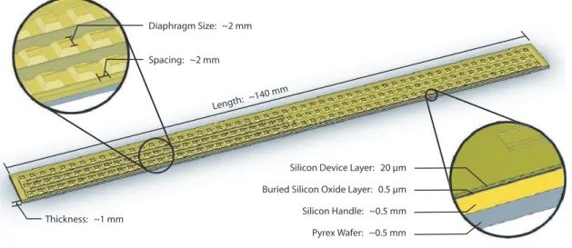
The strain-gauge pressure sensor system presented in this thesis consists of a set of MEMS pressure sensors with side lengths on the order of 2 mm (2000 µm) spaced a few millime-ters apart and fabricated on bonded silicon and Pyrex wafers. The pressure-sensing array was fabricated in silicon and Pyrex for two primary reasons: the structural and electronic properties of these materials, as well as their microfabrication technologies, are stable and well understood. Additionally, silicon offers a controlled environment in which to develop a pressure-sensing array. A future design of the pressure sensor system will take place in polymer materials. The use of a strain gauge instead of silicon-specific technologies, such as piezoresistors, is a design decision that renders the sensor transferrable to polymer-based technologies. These sensors can be arranged over a surface in various piecewise linear con-figurations, such as a single line, a patch consisting of several parallel lines or specialized forms to approximate the shape of a vehicle’s hull or fins. Figure 2-1 shows one possible configuration for the pressure system.
Length: ~140 mm
Thickness: ~1 mm
Diaphragm Size: ~2 mm
Spacing: ~2 mm
Silicon Device Layer: 20 µm Buried Silicon Oxide Layer: 0.5 µm Silicon Handle: ~0.5 mm Pyrex Wafer: ~0.5 mm
Figure 2-1: Diagram of pressure-sensor array with basic structure depicted.
2.1. OVERVIEW OF DEVICE FEATURES 41 narrow1 snaking resistors, mounted on a flexible thin (20 µm) square silicon diaphragm attached at the edges to a square silicon cavity 2000 µm wide on each side. To create a spatially-invariant reference pressure across the array, the cavities are interconnected to one another through channels in both the silicon and Pyrex wafers. As the difference in pressure above and below a particular diaphragm changes, the diaphragm bends2 and the strain-gauge resistances change. To maximize the pressure sensitivity, the four resistors, each on the order of 10 kΩ, are connected in a Wheatstone bridge configuration, which is described later in Section 2.4. A side view of one sensor built in a 150-mm diameter silicon-Pyrex wafer pair is shown in Figure 2-2. There are dozens of such sensors on a single pair of wafers. The square diaphragm is the portion of the silicon suspended above the cavity. The four strain-gauge resistors of the Wheatstone bridge sit on the upper electrically insulating silicon oxide layer. The oxide layer at the bottom surface of the diaphragm serves as an etch stop for wet etching the 650-µm thick silicon handle wafer, and the silicon nitride layer that encases the silicon-oxide-silicon sandwich wafer is the etch mask. This etch process is discussed in Section 3.4. While not shown in Figure 2-2, a waterproofing layer can also be added over the resistors to electrically insulate the devices when they are placed underwater. Each sensor is powered by a common source voltage of 10 V.3 As calculated later in
Section 2.8, the sensitivity of each sensor is thus on the order of 0.087 µV/Pa. Since the thermal noise voltage is near 0.13 µV, the pressure resolution of the sensors is on the order of 1.5 Pa, which satisfies the resolution specification discussed in Chapter 1. The power consumption of each sensor is about 4 µW. If we expect large pressure signals, we can sacrifice pressure resolution and reduce power consumption by lowering the source voltage. Finally, the resonant frequency is 71 kHz, far higher than required for underwater navigation.
The voltage output from the Wheatstone bridges can be quite small, on the order
1For clarity, the following terms are used to describe physical dimensions. Horizontal length: long/short. Horizontal width: wide/narrow. Vertical height: thick/thin.
2As discussed later in Section 2.6, we assume pressure changes that are fractions of an atmosphere, so the diaphragm deflection is much less than the diaphragm thickness.
3However, to increase sensitivity, the tests described in Section 4.5 were performed with source voltages around 20 V.
Pyrex Silicon Nitride Oxide Silicon Oxide Resistor 150 mm 2000 um 500 um 650 um 20 um Top view Air cavity
Figure 2-2: Side view of a single sensor (not to scale). The diaphragm, outlined by the red square, is the portion of the silicon layer above the cavity. (Inset) Four long and narrow resistors (black) sit on the upper oxide layer (orange).
of microvolts. Therefore, in order to improve the signal-to-noise ratio of the sensor, we amplify the signal with a simple measurement chain: a pair of sensing wires attached to the bridge output of each sensor. Each pair of wires is fed into a set of off-wafer amplifying circuits for data analysis. Another scheme for amplification is a set of integrated single-stage differential amplifiers transistor circuits built into the wafer, one for each pressure sensor. This integrated circuit is discussed in Section 5.3.
2.2. WAFER-LEVEL DESIGN 43
2.2
Wafer-Level Design
The wafer-level features of the pressure sensor systems designed and fabricated for this thesis are described here. In all, five rounds of devices were developed to test various combinations of components of the sensor system described in Section 2.1.
1. Pressure-activated diaphragms without strain-gauge resistors; 2. Electrically isolated strain-gauge resistors on dummy wafers;
3. Electrically isolated strain-gauge resistors on pressure-activated diaphragms;
4. Fully interconnected strain-gauge sensors on pressure-activated diaphragms without amplifying transistors;
5. Fully interconnected strain-gauge sensors on pressure-activated diaphragms with am-plifying transistors.
Rounds 1, 2, 3 and 4 have been fabricated and tested. Round 1 demonstrated the suitability of thin silicon diaphragms for sensing pressure. Round 2 showed that our resistor design can be reliably and repeatedly fabricated. Round 3 showed that the strain-gauge resistors can act as pressure sensors. Round 4 enabled the devices to be used underwater. Round 5, left as future work, will reduce the noise and enable x-y addressing to allow for more efficient use of input and output wires by integrating amplifier and array read-out circuitry directly on the wafer.
2.2.1 Air channels
As discussed in Chapter 1, one of the challenges in designing the pressure sensor array is the equilibration of back pressure, which is pressure applied to the back-side of the diaphragms from within the sensor cavity. Since we are interested in detecting the small-signal pressure across the entire array, we increase our signal-to-noise by removing the large-signal pressure (DC component) via a common back pressure. We designed fluidic channels that enable the
back pressure to respond quickly to large-scale overall changes in pressure, such as those experienced when the entire system moves up or down relative to sea level.
Figure 2-3 shows a schematic of such a channel system. The sensor cavities are all connected to the long, snaking air channel, which opens to the ambient water. As the sensor array is lowered in water, the water pressure around the wafer increases, thus pushing water into the channel. As the air-water interface in the channel moves to a new equilibrium, the air pressure in the cavities and channel adjust to balance the increase in water pressure. Thus, the diaphragms, which measure the pressure difference between their local external environment and the common air pressure in the cavities, do not experience the large-signal pressure change. The channel is shaped with a constricted section such that the mechanics of air flow acts as a lowpass filter. The benefit of this filter is discussed in Section 2.9.
Figure 2-3: Schematic of air channels for underwater sensors.
2.2.2 Round 1
Round 1 devices are isolated diaphragms without strain-gauge resistors. Each wafer set consists of nine identical columns of diaphragms. Each column has ten diaphragms; two each of diaphragm sizes 1000 µm (1 mm), 1414 µm, 2000 µm, 2828 µm and 4000 µm. The overlay of the wafer-level features is presented in Figure 2-4. The air channels are etched in Pyrex and connect all the cavities in a column together. The nine columns of air cavities are isolated from one another.
2.2. WAFER-LEVEL DESIGN 45 The wafer is diced into isolated columns, and one diaphragm in each column is deliber-ately pierced. We interface the air channel to a syringe-controlled manometer4 via copper tubes glued to the broken cavity. The manometer manipulates and measures the back pressure, deflecting the diaphragm. Round 1 devices confirm that the deflection behavior of the diaphragm is sufficiently consistent and sensitive to act as the mechanical sensing component of the strain-gauge sensor.
2.2.3 Round 2
Round 2 simply consists of isolated strain-gauge resistors on dummy wafers. Each resistor has large probe pads on each end. The cell-by-cell layout corresponds to that of Round 1 and the resistor layout is presented in Figure 2-5. The inset shows a single cell of resistors and access pads for a 4 mm device. The design of the strain-gauge resistors is discussed in Section 2.7. The resistors are visually examined under a microscope and their resistances are measured.
Figure 2-4: Overlay of Round 1 devices (actual size). The wafer is 150 mm in diameter. The air channels (blue) are etched in Pyrex and connect all the cavities in a column together. The bases of the cavities (red) are slightly wider than the diaphragms (black).
2.2. WAFER-LEVEL DESIGN 47 4 mm 10 mm Diaphragm R1 R2 R4 R3
Figure 2-5: Layout of resistors from Rounds 2 and 3. The wafer is 150 mm. (Inset) Resistors and access pads of one 4 mm cell. The boundary of the diaphragm is dashed in red.
2.2.4 Round 3
Round 3 combines the first two rounds to build isolated strain-gauge resistors on pressure-activated diaphragms. Two classes of Round 3 devices are fabricated.5 Round 3a devices
combines the resistor design of Round 2 (Figure 2-5) with the diaphragms and large air channels etched in Pyrex of Round 1 (Figure 2-4). Round 3b modifies the air channels to thin and narrow channels etched in silicon. The overlay of the wafer-level features is presented in Figure 2-6. The thin and narrow channels alternate sides of the column to reduce the risk of the silicon wafer from breaking. To further mitigate the risk, the silicon channels do not run to the silicon cavities. Instead, the small gap is bridged by slight square etches in Pyrex. Another improvement with Round 3b is the removal of the four sensors at the corners of the wafer. The reason for this minor change is explained at the end of Subsection 3.4.3.
The deflections of the diaphragms are manipulated as described in earlier for Round 1 by a manometer through a deliberately pierced cavity. Additionally, microscope probes are attached to the resistor probe pads to electrically access the sensor as pressure is applied from the back-side. Results from these experiments are discussed in Sections 4.3, 4.4 and 4.5.
5In addition to the design of the air channels, the fabrication processes for the two classes differed as well. This is discussed in Section 3.2.
2.2. WAFER-LEVEL DESIGN 49
Figure 2-6: Overlay of Round 3b devices (actual size). The wafer is 150 mm in diameter. The air channels (red lines) are etched in silicon. The air channels are bridged to the cavity bases (red squares) by small etches in Pyrex (blue squares). The bases of the cavities (red squares) are slightly wider than the diaphragms (black).
2.2.5 Round 4
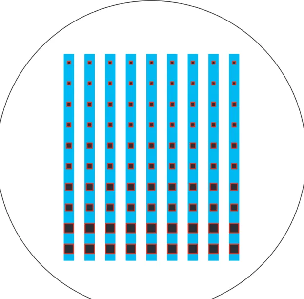
In this set of devices, the sensors are no longer isolated and are instead each wired up on-wafer in a Wheatstone bridge configuration. The sensors are powered and accessed via a custom-made Tech-Etch cable system (discussed later in Section 4.2) that electrically contacts the connection pads on the silicon wafer at one end. The wiring layout is shown in Figure D-13 in Appendix D.
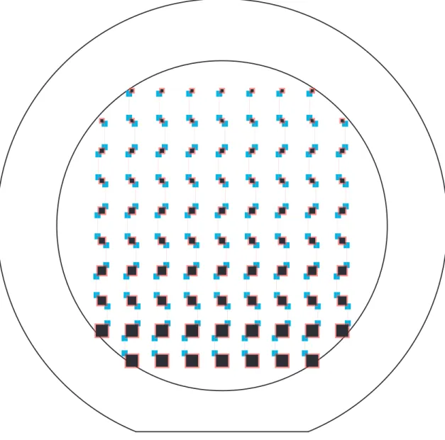
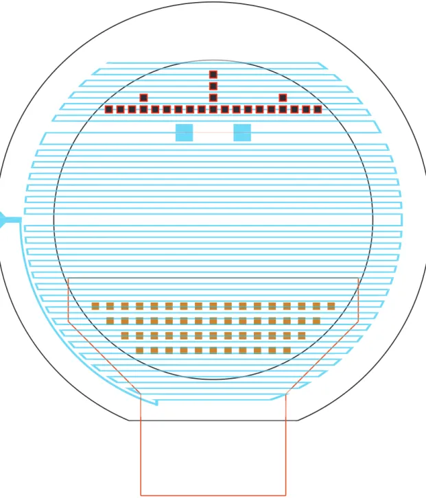
Each Round 4 wafer consists of 24 sensors with 2000 µm square diaphragms, spaced by 2000 µm. The layout can be found in Figure D-12 in Appendix D.6
A single snaking air channel is etched into the Pyrex wafer to connect the cavities under all the diaphragms. Since the channel exits to the environment, water is free to flow into the channel but the channel is long enough that water cannot reach the cavities under the diaphragms. A constricted section in the channel lowpass filters the air flow. As the entire wafer is lowered or raised underwater, the water-air interface in the channel shifts accordingly, which removes the common large-signal change in pressure experienced by all the sensors. Thus, the pressure across each diaphragm remains within the range of the sensors and the sensors are sensitive only to small signal changes. 1 µm of Parylene polymer is added to the top layer of the wafer as a waterproofing material. The wafer is mounted onto a plastic holder for support and control of flow. The entire system can then be placed underwater to detect local changes in pressure.
Figure 2-7 shows the wafer-level layout for Round 4 devices. Preliminary tests on these devices are discussed in Section 4.6.
2.2.6 Round 5
The proposed wafer-level layout of the fully interconnected strain-gauge sensors on pressure-activated diaphragms with amplifying transistors is discussed in Section 5.3.
2.2. WAFER-LEVEL DESIGN 51
Figure 2-7: Overlay of Round 4 devices (actual size). The wafer is 150 mm in diameter. The snaking air channel (blue) is etched in Pyrex and connect all the cavities together. The channel also has a constricted section that acts as a lowpass filter (narrow red line between large blue squares). The bases of the cavities (red) are slightly wider than the diaphragms (black). The 56 access pads (orange) are at the bottom. The Tech-Etch cable (outlined in red) is overlaid on those pads.
2.3
Properties of Silicon
The properties of silicon relevant for modeling device behavior and designing the fabrication process are described here. First, the standard Miller indices, which indicate the directions within a crystalline structure, are defined. Then, the elastic properties, namely Young’s modulus (Eij), Poisson’s ratio (νij) and the shear modulus (Gij), are listed.
2.3.1 Crystalline structure of silicon
Directions and planar orientations of silicon wafers are presented throughout this thesis using standard Miller indices. Directions within a silicon crystal are indicated in brackets [xyz] as if specifying a vector, where x, y and z are the components along those lattice axes. Negative numbers are indicated with a bar above the absolute value. For example, [011] represents the direction parallel to the vector (0, 1, −1). Likewise, planes are specified using parentheses, where (xyz) specifies the plane normal to the [xyz] direction. Figure 2-8 illustrates three distinct pairs of directions and corresponding planes.
[110]
Figure 2-8: Crystal planes and major directions. The shaded areas represent crystal planes and the vectors indicate crystal directions. Reproduced from [66].
Because of the lattice symmetry, certain sets of directions or planes are equivalent. Angle and curly brackets denote such degenerate directions and planes, respectively. For example, the [100], [010] and [001] directions are called h100i directions, and the (100), (010) and (001) planes are called {100} planes. The orientation of the silicon wafer with
2.3. PROPERTIES OF SILICON 53 respect to the crystal lattice affects the results of various wafer chemical processes as well as the mechanical properties of structures built from the wafer.
Wafers are identified by the plane of their top surface, or face. All silicon wafers described in this thesis are standard 150-mm diameter (100) wafers with wafer x, y and z coordinates7
along the [011], [011], and [100] directions of the crystal lattice, respectively, where x is parallel to the wafer flat, y is perpendicular to the wafer flat and in the plane of the wafer face, and z is out of the wafer face (Figure 2-9).
Figure 2-9: Crystal orientation in (100) silicon wafers showing (a) the direction normal to the surface, and (b) the directions of the wafer x and y axes. The wafer x axis is parallel to the wafer flat. Reproduced and corrected from [45].
2.3.2 The elastic properties of silicon
The behavior of the silicon-based pressure sensors is dependent on silicon’s elastic properties. Furthermore, as an anisotropic material, silicon’s Young’s modulus (Ei), Poission’s ratio (νi)
and shear modulus (Gij) depend on its crystal orientation. For example, possible values of
Young’s modulus range from 130 to 188 GPa, and those for Poisson’s ratio range from 0.048 to 0.40 [45]. These three elastic measures are related to the compliance matrix (S), which
7Note that there are two sets of axes named “x-y-z”: the crystal lattice and the wafer. The use of the same symbols is unfortunate, but common in microfabrication literature. Context should make the meaning clear.
describes the relationship between strain8 (ǫij) and stress (σij) in the form of Hooke’s law:
~ǫ = S~σ. Although a homogeneous, mechanically conservative9, but generally anisotropic
material has at most 21 independent constants in its compliance matrix, symmetry can reduce this number. Due to its cubic structure, silicon exhibits orthotropic elastic properties, i.e. there exist three orthogonal axes where the shear and axial components of stress and strain are decoupled. Therefore, the orthotropic form of Hooke’s law is
ǫxx ǫyy ǫzz ǫyz ǫzx ǫxy = 1 Ex − νyx Ey − νzx Ez 0 0 0 −νxyEx Ey1 −νzyEz 0 0 0 −νxzEx −νyzEy Ez1 0 0 0 0 0 0 2Gyz1 0 0 0 0 0 0 2Gzx1 0 0 0 0 0 0 2Gxy1 σxx σyy σzz σyz σzx σxy , (2.1)
where the conservative property requires the compliance matrix to be symmetric:
−νxy Ex = −νyx Ey , −νxz Ex = −νzx Ez , −νyz Ey = −νzy Ez . (2.2)
Thus, orthotropic decoupling reduces the number of independent constants in S from 21 to 9. For standard (100) silicon, the symmetry between the x and y axes, which are both along h110i directions, further reduces the number of independent constants to 6 [45]:10
Ex = Ey = 169 GPa, Ez = 130 GPa, (2.3)
νyz = νxz = 0.36, νzx = νzy = 0.28, νxy = νyx = 0.064, (2.4)
Gyz = Gzx = 79.6 GPa, Gxy = 50.9 GPa. (2.5)
8In this thesis, the term shear strain refers strictly to pure shear strain, not engineering shear strain. 9A material is mechanically conservative if the work done to strain it is independent of the physical path taken.
10Although 7 values are listed here, the two values of ν
ijinvolving the z direction, 0.36 and 0.28, are not independent of each other. They are related through the conservative property as described in Equations 2.2. To go further, a perfectly isotropic material, that is one whose mechanical properties are completely identical regardless of orientation, has only two independent elastic constants: the Young’s modulus (E) and the Poisson’s ratio (ν). Its shear modulus is related to them by G = E


![[PDF] Formation PrestaShop : Module TNT Express | Formation à télécharger en PDF](data:image/gif;base64,R0lGODlhAQABAIAAAP///wAAACH5BAEAAAAALAAAAAABAAEAAAICRAEAOw==)