ARCING MITIGATION AND PREDICTIONS FOR HIGH VOLTAGE SOLAR ARRAYS
by
Renee Lynn Mong S.B. Aeronautics and Astronautics Massachusetts Institute of Technology, 1991
Submitted to the Department of
Aeronautics and Astronautics in Partial Fulfillment of the Requirements for the
Degree of
MASTER OF SCIENCE in Aeronautics and Astronautics
at the
Massachusetts Institute of Technology June 1993
@Massachusetts Institute of Technology 1993 All Rights Reserved
Signature of Author
Department of Aeronautics and Astronautics May 7, 1993
Certified by
Professor Daniel E. Hastings, Thesis Supervisor SDepartment of Aeronautics and Astronautics Accepted by
Professor Harold Y. Wachman, Chairman Department Graduate Committee
Aero
MASSACHUSETTS INSTITUTE
OF TECHNOLOGY
ARCING MITIGATION AND PREDICTIONS FOR HIGH VOLTAGE SOLAR ARRAYS
by
Renee Lynn Mong
Submitted to the Department of Aeronautics and Astronautics on May 7, 1993 in partial fulfillment of the
requirements for the Degree of Master of Science in Aeronautics and Astronautics
Future solar arrays are being designed for much higher voltages in order to meet high power demands at low currents. Unfortunately, negatively biased high voltage solar cells have been observed to arc when exposed to the low earth orbit plasma environment. Analytical and numerical models of this arcing phenomenon on conventional solar cells have been developed which show excellent agreement with experimental data. With an understanding of a mechanism for arcing, it is possible to determine methods of arc rate mitigation and to predict arc rates for experiments. Using the previously developed models, it was determined that the arcing rate can be decreased by (1) increasing the interconnector work function, (2) increasing the thickness of the coverglass and cover adhesive, (3) decreasing the secondary electron yield of the coverglass and adhesive, (4) decreasing the ratio of the coverglass/adhesive dielectric constants, and (5) overhanging the coverglass. Of these, methods (4) and (5) show the most promise in reducing or even eliminating arcing. In addition, arcing rates were predicted for the high voltage biased arrays of the Air Force's Photovoltaic and Space Power Plus Diagnostics exper-iment (PASP Plus) and NASA's Solar Array Module Plasma Interactions Experexper-iment (SAMPIE). These predictions provide both expectations for the missions and a means to test the numerical and analytical models in the space environment for different solar cell technologies. Finally, a numerical model of the arc initiation process was also developed for wrap-through-contact cells, but experimental data is not available for comparisons.
Acknowledgements
I must first thank my thesis advisor, Professor Hastings, for his support and guidance. His initial encouragement made me believe I could accomplish everything he said that could be done, his assistance in pinpointing problems helped me immensely, and his excitement over my successes equaled my own.
I am also in great debt to Scott for patiently listening to me, for lifting my spirits countless times, for doing so many things to make my life easier, and for just being himself. He has filled my life with more happiness than I ever dreamed possible. I have no doubt that he has caused me to be more productive and more sane these past two years. I also have him to thank for keeping me here at MIT when I thought I was ready to leave.
Although they may never fully understand what I've done, my parents are also re-sponsible for my success. They have always encouraged me to be my best, and they were always there to applaud my achievements. They taught me to reach for the stars and to be proud of the height I attain. I will always be thankful they are my parents.
Without family and friends, life would be too lonely for me. I am particularly thankful for my wonderful sister who has certainly made my life more enjoyable and entertaining. I only wish we lived closer so I could watch her grow up more often. The friends made in graduate school have each helped me and brightened my life in their own ways. John helped me with homework, actually understood me when I talked about my research, and encouraged me to practice his philosophy that you can't possibly accomplish anything in the 30 minutes or so before a class or meeting. Pam always gave me something to smile about, and Jackie saved me from a weekend of despair. Ray, whom I pestered and teased all year, finally realized it was all in good fun and became one of my closest friends when I really needed one.
Contents
Acknowledgements 1 Introduction
1.1 Background ... . . . ... 1.2 Overview of This Research . ...
2 Numerical and Analytical Models 2.1 Conventional Solar Cells ..
2.1.1 Numerical Model . . 2.1.2 Analytical Model . . 2.2 Wrap-Through-Contact Cells 3 Arc Mitigation Methods
3.1 Control Case...
3.2 Interconnector Material . . . 3.3 Dielectric Thickness ... 3.4 Secondary Electron Yield . .
3.5 Dielectric Constants ... 3.6 Overhanging the Coverglass
3.6.1 Numerical Results . . 3.6.2 Analysis ... 3.7 Arc Rate Results ...
4 PASP Plus and SAMPIE Predictions 4.1 PASP Plus ... 4.1.1 Experiment Description . 4.1.2 Predictions ... 4.2 SAMPIE ... 4.2.1 Experiment Description . 42 . . . . 42 . . . . . . 45 . . . . . . 47 . . . . . . 48 . . . . 50 . . . . . . 54 . . . . . . 54 . . . . 58 . . . . 61 66 . . . . 66 . . . . . . 67 . . . . . . 69 . . . . 79 . . . . . . 79
j I : : : :
... . . . . . . . . . . . . . . . . . . . ... °... ... . . . . . . . . . . . . . . . . . . . . . . . . . . . . . . . . . . . . . . . .4.2.2 Predictions ... ... 83
5 Conclusions 85
5.1 Summary of Results ... ... 85
List of Figures
1.1 Schematic of a conventional solar cell ... . . . . . 13
1.2 Model of the conventional solar array used for numerical simulations . . 16
1.3 Arcing seqence of a high voltage solar array . ... 18
2.1 Model system of the high voltage solar array and plasma interactions . 22 2.2 Grid structure for conventional cell calculations . ... 23
2.3 Typical electric potential contour plot for ambient ion charging of con-ventional cells . . ... .... ... .... ... . ... . . ... . . 25
2.4 Typical surface charge density along side dielectrics after ambient ion charging of conventional cells ... . ... . . . . . 25
2.5 Electric field lines over a whisker on conductor surface ... 26
2.6 Geometry for EFEE charging ... . . . . 28
2.7 Typical electric field run-away versus time ... ... . 29
2.8 Experimental data for ground and flight experiments ... . . 32
2.9 Schematic of a wrap-through-contact solar array ... . 33
2.10 Wrap-through-contact solar array model used for numerical simulations . 34 2.11 Typical grid structure for calculations ... . . . . 35
2.12 Typical electric potential for ambient ion charging of WTC cells ... 36
2.13 Typical surface charge density along the side dielectric surface after am-bient ion charging of WTC cells ... ... 37
2.14 Class 1 electric field at upper triple junction versus time ... 38
2.15 Class 2 electric field at upper triple junction versus time ... 39
2.16 Class 1 surface charge density over the coverglass (a) side surface, (b) front surface ... ... .. .. 40
2.17 Class 2 surface charge density over the coverglass side surface ... 41
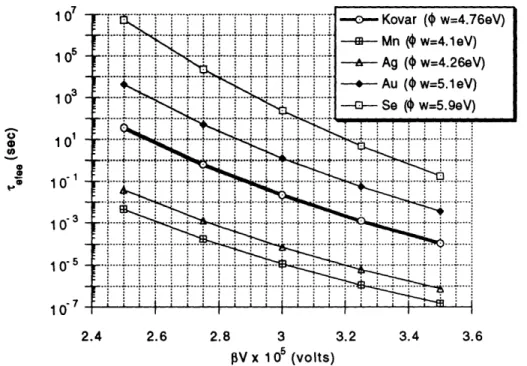
3.1 Enhanced field electron emission charging time, Tefee, versus pV for the silicon conventional control case . . . . .. . . . . 44
3.3 Enhanced field electron emission charging time, rf,ee, versus /V for
different work functions,
4
(eV) ... . . . . 463.4 Analytic predictions and numerical results for refee/Tefee(ow = 4.76eV) versus pV ... ... 46
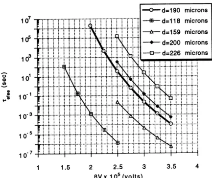
3.5 Enhanced field electron emission charging time, rfee,, versus /V for different dielectric thicknesses, d(jim) ... . . . . 47
3.6 Analytic predictions and numerical results for Tefee/Tefee(d = 19o0m) ver-sus 3V ... 48
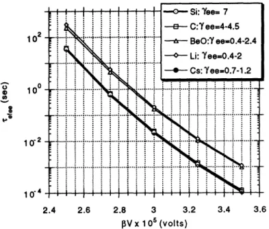
3.7 Enhanced field electron emission charging time, Tefle, versus PV for different secondary electron yields, %-y ... . . . . 49
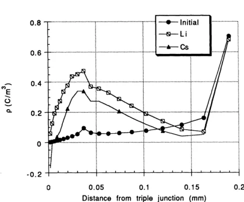
3.8 Surface charge density as a function of distance from the triple junction for different secondary electron yields, yee . ... . . . 50
3.9 Enhanced field electron emission charging time, refee, versus OV for different dielectric constant ratios ... . . . . 51
3.10 Dielectric side surface charge density before EFEE charging for different dielectric constants ... ... 52
3.11 Electron trajectories for Edl, lfa = 2.7 . ... . . . . 53
3.12 Electron trajectories for the control case of Ed /ead = 1.3 . . . . 53
3.13 Electron trajectories for ea,/Cda =0.74 ... . . . .... 54
3.14 Average secondary electron yield over the adhesive versus time for dif-ferent dielectric constants ... ... 55
3.15 Model of coverglass overhang ... . . . . 55
3.16 Enhanced field electron emission charging time, reee,, versus [IV for different overhang lengths ... 56
3.17 Class comparison of Tfe,, versus ETJ for 3V = 3.5 x 10⁵V ... . 57
3.18 Electron trajectories for 10ipm overhang; /V = 3x10⁵V ... 57
3.19 Electron trajectories for 50pm overhang; 3V = 3 x 10V ... 58
3.20 Class 1 dielectric surface potential; PV = 3 x 10⁵V, do = 10ptm ... 59
3.21 Class 2 dielectric surface potential; 3V = 3.25 x 10⁵V, d, = 50pm . . . . 59
3.22 Analytic arc rates for varying interconnector work functions, O ... .62
3.23 Analytic arc rates for varying dielectric thicknesses, d ... . 62
3.24 Predicted arc rates for varying secondary electron yields, -Y, ... 63
3.25 Predicted arc rates for varying dielectric constant ratios, Ed,/E a . . . . 64
3.26 Predicted arc rates for varying coverglass overhang lengths, do (pm) . . . 65
4.2 Selected arc rate predictions with standard deviation errors for Si conven-tional array #1 ... 73 4.3 Complete arc rate predictions in the differentiating voltage range for Si
array #1 ... 73
4.4 Selected arc rate predictions with standard deviation errors for Si
conven-tional array #2 . . . . 74 4.5 Complete arc rate predictions in the differentiating voltage range for Si
array #2 . . . . 74 4.6 Selected arc rate predictions with standard deviation errors for GaAs/Ge
conventional array #4 ... 75 4.7 Complete arc rate predictions in the differentiating voltage range for
GaAs/Ge array #4 ... ... 75 4.8 Selected arc rate predictions with standard deviation errors for GaAs/Ge
conventional array #6 ... .. 76 4.9 Complete arc rate predictions in the differentiating voltage range for
GaAs/Ge array #6 ... ... 76 4.10 Selected arc rate predictions with standard deviation errors for GaAs/Ge
conventional array #11 ... ... 77 4.11 Complete arc rate predictions in the differentiating voltage range for
GaAs/Ge array #11 ... 77
4.12 Selected arc rate predictions with standard deviation errors for APSA (#36) 78
4.13 Complete arc rate predictions in the differentiating voltage range for
A PSA (#36) . . . .. . . . 78 4.14 Arc rate prediction comparison for all PASP Plus conventional arrays at
350km . . . 80 4.15 SAMPIE experiment package ... 81 4.16 SAMPIE experiment plate layout ... .... 82 4.17 SAMPIE arc rate predictions with standard deviation error bars for the
List of Tables
3.1 Conventional silicon cell data used in numerical simulations ... 43 4.1 PASP Plus data used for arc rate predictions ... 70
List of Symbols
A Fowler Nordheim coefficient (1.54 x 10- 6 x 104.520W/qw A/V2)
B Fowler Nordheim coefficient (6.53 x 10⁴/-5 V/m)
Cdiele capacitance of dielectric (F/m2)
Cfront capacitance of coverglass front surface (F) d thickness of dielectric (m)
di thickness of coverglass (m)
d2 thickness of adhesive (m)
dg,,p gap distance between cathode and anode (m)
dt distance of electron first impact point from triple junction (m)
do overhang distance of coverglass (m)
dc critical overhang distance of coverglass (m)
Ee electric field at emission site (V/m)
E electron incident energy on dielectric plate (eV)
E,, electron incident energy for maximum secondary electron yield (eV) ET electric field at triple junction (V/m)
E, electric field of coverglass (V/m)
E2 electric field of adhesive (V/m)
jec electron current density from conductor (A/m2)
jee secondary electron current density from dielectric (A/m2)
jFN Fowler-Nordheim current density from the conductor (A/m2)
jid ion ram current density to the dielectric (A/m 2) ne plasma number density (m-3)
n., emission site number density (m- 2)
me electron mass (kg)
mi ion mass (kg)
R arc rate (sec- 1)
r8 sheath radius (m)
SFN emission site area determined from F-N plot (m2
Sra emission site area determined by accounting for electron space charge effects (m2
)
Te electron temperature (eV)
T ion temperature (eV)
Varc voltage at which last arc occurred V
Vbi, bias voltage of interconnector/conductor V V voltage which minimizes arcing time V
Vi initial voltage before solar cell charging V
v,, mean speed of ions entering sheath (m/sec) vX electron velocity in the x direction (m/sec)
vy electron velocity in the y direction (m/sec)
y distance of emission site from the triple junction (m)
P field enhancement factor
AQ charge lost from one coverglass by one discharge (C) ed, relative dielectric constant of coverglass
E relative dielectric constant of adhesive 61 energy at ,,ee = 1 (eV)
Oc potential of conductor (V)
O, potential of coverglass-adhesive interface (V) OW work function (eV)
7ee secondary electron yield
y7 maximum secondary electron yield at normal incidence
77 factor accounting for difference in electric field at emission site and triple junction
0O incident impact angle of electron onto the dielectric surface
a surface charge density (C/m2)
Tare time between arcs (sec)
re fee EFEE charging time (sec)
rion ion charging time (sec) Tex7 experiment time (sec)
Sfactor
accounting for difference of dielectric constants between coverglass and adhesiveChapter 1
Introduction
In the past and present, solar arrays used in space have been operating at low voltage levels, typically biased at 28V. Future solar arrays, however, are being designed for much higher voltages in order to meet high power demands of the order of 10kW to 1MW. High current levels could be used instead to achieve these increased power demands, but the power distribution cables would need to be more massive and the resistive losses would be greater. Consequently, the current is maintained at a low value while the voltage is increased to attain the necessary power level.
A schematic of a conventional solar cell is shown in Fig. 1.1. The coverglass and sub-strate shield the solar cell from the environment, mainly to reduce radiation degradation. These are attached to the cell with adhesives. The solar cell itself is a semiconductor of two parts, a p-type semiconductor which has an abundance of electrons and an n-type semiconductor which has an abundance of electron holes. This construction allows the solar cell to use the photoelectric effect to convert solar energy into electric power. A photon with energy equal to or greater than the energy gap of the solar cell it enters will free an electron. This creates an electron-hole pair. If the pair is in the p-type semicon-ductor, the electron will be accelerated across the p-n barrier to the n-type semiconductor where it will recombine. The hole, however, will be repelled by the barrier because of the excess of holes in the n-type semiconductor. Likewise, if the electron-hole pair is in the n-type semiconductor, the hole will be accelerated across the p-n barrier and the electron repelled. Consequently, metal interconnectors connect the n-type semiconductor of one cell to the p-type semiconductor of the adjacent cell to utilize the current created by the electron and hole movement. Solar cells are connected in parallel with metal interconnectors to obtain desired current levels and connected in series to obtain desired voltage levels.
The solar array, along with other surfaces of the spacecraft which can allow the passage of current, collects current from the ambient plasma. In steady state, the spacecraft is
Coverglass
Adhesive
P_ nSolar
CellInterconnector
Substrate
Figure 1.1: Schematic of a conventional solar cell
grounded with respect to the plasma by the zero net charging condition
Op
t+ Vj= O, (1.1)
which is derived from Ampere's Law and Gauss's Law. To obey this condition, most of the solar array floats negatively with respect to the plasma This is because the random thermal flux of the lighter electrons to the spacecraft is greater than the random flux of the heavier ions. Therefore, the spacecraft surfaces must be negatively biased in order to maintain zero net current collection.
High voltage solar arrays, however, have been observed to interact with the plasma environment of low earth orbit in two undesirable manners. For positive voltages, the
current collection can be anomalously large, possibly leading to surface damage [25].
This phenomenon, known as "snap-over", occurs when the dielectric surface potential becomes positive, attracting electrons. Above a certain potential, more than one secondary electron is released by the incident electrons. These excessive secondary electrons are collected by the interconnector and seen as a current increase, which then incurs a power loss. For large negative voltage biases, arc discharges can occur [11]. Arcing observed in experiments has been defined as a sharp current pulse much larger than the ambient current collection which lasts up to a few microseconds. This current pulse is usually accompanied by a light flash at the edge of the solar cell coverglass. Arc discharges can cause electromagnetic interference and solar cell damage [26], so there is a need to study mitigation methods and to be able to predict arcing rates with models.
1.1
Background
Arcing has been studied in many experiments and theoretical arguments. The Plasma Interactions Experiments have been the only space experiments so far, though several
space experiments are planned for the near future. Arcing has also been observed in many ground tests conducted in vacuum plasma chambers. Two different theoretical explanations were given by Parks et al. [21] and Hastings et al. [10]. Cho and Hastings [3] used ideas from both to present a more complete theory of the arcing sequence of events.
Arcing on solar cells was originally observed by Heron et al. [11] in 1971 during a high voltage solar array test in a plasma chamber. The array was biased to -16kV, and arcing was observed as low as -6kV in a plasma density of 108m- .
In 1978, the first Plasma Interactive Experiment (PIX) [6] confirmed that arcing occurs in space. As an auxilliary payload on Landsat 3's Delta launch vehicle, PIX operated for 4 hours in a polar orbit around 920km. A solar array of twenty-four 2cmx2cm conventional silicon cells was externally biased to -1000V. Arcing discharges began at -750V.
In 1983, PIX II [7] was launched also as an auxilliary payload aboard a Delta launch vehicle into a near circular polar orbit of approximately 900km in altitude. The five hundred 2cmx2cm silicon conventional cells, biased to -1000V, experienced arcing as low as -255V and at densities as low as 103cm- 3. The results also found arcing to be the most detrimental effect of negative biasing.
Ferguson [4] studied the PIX II ground and flight results. The interconnectors collected current proportional to the applied voltage bias. The arc rate R was determined to scale
as
R ne 1/2) Vas, (1.2)
where a - 5 for the ground experiments and a _ 3 for the flight experiments, n, is the ambient plasma number density, T is the ambient ion temperature, and mi is the ambient plasma ion mass. The dependence of the arc rate on these parameters indicates that the coverglass surface is recharged by the thermal flux of ions.
Ground experiments revealed more characteristics of the arcing phenomenon. Exper-iments by Fujii et al. [5] showed that dielectric material near the biased conductor in the plasma environment is essential for arcing to occur. Fujii et al. tested material plates biased to high negative voltages in a plasma environment. The plate partially covered by a 200[tm thick coverglass experienced arcing at -450V while the uncovered plate did not arc, except at -1000V when the arc occurred at the substrate. Snyder [22] measured the electric potential on the coverglass and found that it decreased significantly when an arc occurred. This indicates that the negative charge created during arcing discharged the positive surface charge accumulated on the coverglass surface. Both Snyder and Tyree
[23] and Inouye and Chaky [15] observed electron emission from the solar array that could not be explained by the ambient plasma. Finally, electromagnetic waves generated from the arcing current were measured by Leung [19].
The first theoretical model was proposed by Jongeward et al. [16] and later expanded by Parks et al. [21]. Jongeward et al. attributed Snyder's [22] experimental observation of the decrease in coverglass potential prior to arcing to enhanced electron emission from the interconnector, which corresponds to the electron emission observed in Refs. [23] and [15]. They suggested the emission is due to a thin layer of ions deposited on the interconnector, causing the electric field to be significantly increased. The time for positive charge build up is then dependent on the ambient density ne, the interconnector size, and the bias voltage. The arc discharge is proposed to occur by a positive feedback mechanism from electron heating which leads to a space charge limited discharge. At low ion densities, other surface neutralizing effects are said to dominate, thus inhibiting the positive charge build up. Jongeward et al. also modeled the arc discharge decay time by assuming space charge limited conditions and showed that the peak current magnitude agrees well with this assumption.
Parks et al. [21] concentrated on further detailing the theory proposed by Jongeward et al. [16] on the prebreakdown electron emission current. They accepted Jongeward's theory of positive charge build-up in a thin insulating layer on the interconnector and of arcing orginated from interconnector electron emission instead of from the ambient plasma. Parks et al. proposed the addition of the phenomena presented by Latham [17, 18], namely that nonmetallic emission processes are significantly responsible for electron emission by nominally metallic surfaces. Therefore, Parks et al. claimed that the arc rate must be proportional to the electron emission current density and the bias voltage. They further suggested that electron emission is controlled by the vacuum electric field at the surface of the insulator. Given these assumptions, they determined that the rate of field build-up in the insulator is
S( E Eins-ac) = ji + jFN(e" P - ), (1.3)
where eC, is the dielectric constant of the insulator layer, Ei, is the electric field inside the insulator, Ein -,a is the electric field at the insulator-vacuum interface, ji is the ion current density, jFN is the Fowler-Nordheim emission current at the metal-insulator interface, a is the rate of ionization per unit distance inside the layer, d is the thickness of the insulator layer, and P is the probability that electrons are emitted from the
insulator--Coverglass /Triple Junction
Munesve -Interconnector
Figure 1.2: Model of the conventional solar array used for numerical simulations
vacuum interface. The emission current from the metal-insulator interface is given by
jFN = AEns,,e- 7', (1.4)
where A and B are the Fowler-Nordheim emission coefficients, given in Eqns. 1.8 and 1.9. This expression for the electric field accounted for experimental observations of the characteristics of the voltage threshold, the prebreakdown electron emission current, and the arcing rate.
Hastings et al. [10] did not try to explain the prebreakdown electron emission current but instead proposed a model for the gas breakdown seen as the arc discharge. They suggested that neutral gas is desorbed from the sides of the coverglass by electron bom-bardment, a phenomena known as electron stimulated desorption (ESD). The bombarding electrons are emitted from the interconnector, as determined from Snyder's experiments [22], and from the coverglass as secondary electrons which return to the side surface. The desorbed neutrals then accumulate in the gap between the coverglasses over the inter-connector, forming a potentially high-pressure gas layer which can break down from the electron emission current flowing through it. This was in contrast to the previous theory which suggested that the arc occurs in an insulator on the surface of the interconnector. Recent work by Cho and Hastings [3] combined some of the ideas from these two theories and studied the charging of the region near the plasma, dielectric, and conductor triple junction. The model that they studied is shown in Fig. 1.2. The dielectric consists of both the coverglass and the adhesive bonding the coverglass to the solar cell. The conductor is the interconnector, which is usually placed between the cell and substrate on one end and between the cell and cover adhesive in the adjoining cell. The solar cell itself was neglected since the potential drop across it is at most a few volts while the potential drop across the coverglass and adhesive is hundreds or even thousands of volts for high voltage operation.
Cho and Hastings developed a numerical simulation of the arc initiation processes. They studied charging of the dielectric surfaces by three sources: ambient ions, ion-induced secondary electrons, and enhanced field electron emission. From numerical
results, they determined the following arc sequence, illustrated in Fig. 1.3: (1) ambient ions charge the dielectric front surface, but leave the side surface effectively uncharged;
(2) ambient ions induce secondary electrons from the conductor which charge the side surface to a steady state unless enhanced field electron emission (EFEE) becomes significant;
(3) EFEE will charge the side surface if there is an electron emission site close to the triple junction with a high field enhancement factor, /; and
(4) EFEE can result in collisional ionization of neutrals desorbed from the coverglass, which is what is observed as the arc discharge.
They also found that the electric field at the triple junction is not bounded during EFEE charging.
Cho and Hastings used the numerical results to develop analytical formulas describing the arcing rate [3, 9]. They suggested that the time between arcs is the minimum of the sum of the ambient charging time r. and the enhanced field electron emission charging
time refee, so that the arc rate R is given by:
R = min(ron + Tefee) - 1 (1.5)
For the ion charging, Cho and Hastings showed that ambient ions mainly charge the front surfaces of the coverglass, not the side surfaces. They expressed this time as
Tion = e A (1.6)
enevioAa'
where AQ is the charge lost by the coverglass due to an arc discharge, which must be recovered; enevio, is the ambient ion flux to the front surfaces, with vi, as the mean speed of ions entering the sheath surrounding the solar array; and A,,u is the frontal area of the coverglass. Assuming a constant secondary electron yield and constant voltage bias, they derived the following analytical expression for the EFEE charging time, Tefee:
Cdeleci Bd
7efee - 1)VY,-, Cd(i[ A--E exp I (1.7)
where A and B are the Fowler-Nordheim coefficients given by 1.54 x 10-6104.52/VO
A = (1.8)
-
-V interconnector= -V
secondary electron multiplication
enhanced field emission
enhanced field emission
charging
of
front
surface
charging
of side
surface
discharge
recharging
by ions
~
=-Vis a factor to account for the difference in dielectric constants and is given by
d2[ di d-d2)]-1
_= + (1.10)
Co is C evaluated with di = d, d, is the distance from the triple junction of the first impact
by an electron emitted from the conductor, Cdide is the capacitance of the dielectric at this impace site, ey, is the secondary electron yield of the dielectric, Sre, is the real area of the emission site, SFN is the Fowler-Nordheim "effective" area of the emission site, l is a factor to account for the difference in the electric field at the emission site from the triple junction, di is the thickness of the coverglass, d2 is the thickness of the adhesive,
d = dl + d2, V is the voltage at which the arc occurs, and # is the field enhancement
factor. From comparison with experiments, Hastings et al. [9] suggested that / must be greater than a few hundred, so they assumed that the field enhancement is due to a thin dielectric layer on the conductor surface rather than microprotrusions. They later updated their views as explained in Section 2.1.1.
From experimental observations, Hastings et al. [9] suggested other characteristics of the arcing processes, such as the discharge wave hypothesis and the occurrence of one arc at a time within a certain area. The discharge wave hypothesis suggested that at arc initiation emitted electrons form a plasma cloud over the solar array. Some of the electrons, attracted by the positive surface potential, strike the coverglasses in the local area until they are discharged. Experimental results also showed that the arc current is more likely to be carried by electrons, consistent with the hypothesis that arcing is initiated by electron emission from the interconnector. In addition, as the temperature increased fewer neutral gas molecules were desorbed from the dielectrics and the arc rate was seen to decrease, consistent with the hypothesis that ionization of the neutral gases also plays a role in arc initiation.
1.2 Overview of This Research
Power requirements for space systems are increasing significantly. As the most reliable power source, high voltage solar arrays will be needed to meet these requirements. Since arcing degrades the array performance and causes electromagnetic interference which affects nearby instruments, it is imperative to study arcing. Recent studies by Cho and Hastings [3, 9] determined an arcing sequence of events and an arcing rate based on numerical and theoretical work which has been shown to agree well with experimental results. With these models it is possible to determine methods of arc rate mitigation and
to predict arc rates for experiments. This research can then be used in the design of new solar cells and in the design of high voltage solar arrays.
The focus of this research is twofold: to identify and study mitigating effects on arc rates and to present arc rate predictions for two space experiments soon to be launched. In Chapter 2 the numerical and analytical nodels developed by Cho and Hastings are reviewed, and the numerical model modified for the wrap-through-contact solar cell ge-ometry is presented. Based on the analytical model for conventional solar cells, arc rate reduction methods are studied using the corresponding numerical model in Chapter 3. In Chapter 4, arcing rates are predicted for the high voltage biased arrays of the Air Force's Photovoltaic and Space Power Plus Diagnostics experiment (PASP Plus) and NASA's Solar Array Module Plasma Interactions Experiment (SAMPIE). Finally, conclusions are summarized and future work is suggested in Chapter 5.
Chapter 2
Numerical and Analytical Models
2.1 Conventional Solar Cells
A schematic of a conventional solar cell is shown in Fig. 1.1. In high voltage operation, the voltage differential over the coverglass and adhesive can be hundreds or even thou-sands of volts while the voltage differential over the cell itself is at most a few volts. For modeling purposes, the cell semiconductor can therefore be neglected, as shown in Fig. 1.2. In this model, the interconnector is a conductor and the coverglass and adhesive are dielectrics. The numerical and analytical models used for conventional cells were developed by Cho and Hastings [3, 9], as briefly described in Section 1.2.
2.1.1 Numerical Model
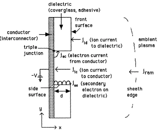
The numerical model incorporates all relevant physical characteristics and processes for solar cell charging from the ambient plasma, electron emission from the interconnector, and secondary electron emission from the dielectrics. A representation of this system is shown in Fig. 2.1. The coverglass and adhesive surface charge densities are affected by the ion ram current density jd, the electron emission current density from the conductor
jee, and the secondary electron current density from the surface jee. After arc initiation,
the current densities from the ionization of neutral gases may also be significant. These are not considered, however, as only the time to arc initiation is the focus of this research. The rate of change of the dielectric surface charge density can then be expressed as
da(xt) = jd(, t)- P(, P, c(yt)dy tdy -- (x, ', t)jee(')d' + jee(X, t), (2.1)
where P(x, y, t) is the probability that an electron emitted from position y on the conductor hit the dielectric at position x at time t, and P(x, x', t) is the probability that an electron
dielectric (coverglass, adhesive) S front ,,, surface -U conductor u#rsc
(interconnector) (ion current
,, ,id (ion current
triple to dielectric)
junction junctionec (electron current
,, from conductor) J-,,, S,, ic (ion current -V ,' to conductor) Jee (secondary side ,, electron on surface d dielectric) x ambient plasma <- Jram sheath edge l'
Figure 2.1: Model system of the high voltage solar array and plasma interactions
The numerical model consists of three schemes. The first scheme uses the capacitance matrix method to obtain a preliminary electric potential distribution along the dielectric surfaces. The second scheme involves a particle-in-cell (PIC) method which is used for ambient ion charging. Once a steady state is obtained from the ion charging, a space-charge-free orbit integration scheme calculates the electron charging by enhanced field electron emission (EFEE).
All schemes use the same computational domain and grid. The phase space of the domain consists of two position coordinates and three velocity coordinates. As shown in Fig. 2.2, the domain includes two halves of solar cells with the interconnector forming the lower boundary of the gap between the cells. The boundary condition far from the cells at x = 0 is 4 = 0, simulating the far field. In these simulations, any electrons leaving the domain at x = 0 will also leave the sheath. The boundaries are thus Dirichlet in the x direction and periodic in the y direction to simulate a solar array. The grid is clustered along the dielectric sides and near the interconnector for better resolution of the large electric potential gradients in these areas.
The capacitance matrix method is used to obtain an inititial condition for the PIC code, thus reducing the simulation time. In employing this method, which is given in
Plasma __ICC
11 1
Coverglass Adhesive .* * 10.0260 10.0112 Y (mm) 9.9964 9.9817 20.5 13.7 Y (mm) 6.8 29.795 29.863 29.932 Interconnector -1 Triple Junction 30.000 X (mm)Figure 2.2: Grid structure for conventional cell calculations
9.726
Ref. [14], a unit charge is ascribed to one cell on the dielectric surface while all other cells have zero charge. The Poisson equation is then solved to determine the electric potential in every cell on the dielectric surface due to this unit charge. This process is repeated for each grid cell along the surface of the dielectrics. Afterwards, the array containing all of the potential values calculated is inverted to determine the capacitance value for each grid cell. This matrix is stored for use as the initial conditions of the PIC code, so that the simulation can be started from any charging state described by only the surface charge or the surface potential.
With the capacitance matrix calculated for unit charges, the PIC code calculates the space potential based on a pre-determined surface potential. The initial conditions for the dielectric potential are 0 = 0 on the front surface and a linear distribution of
4
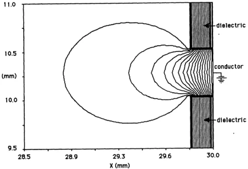
on the side surface with the conductor voltage at one end and the front surface zero voltage at the other end. The ram velocity is oriented 90 to the dielectric front surfaces and conductor. To save computational time, an artificial ion mass is used such that mi/me = 100. Ions and electrons are initially inserted uniformly throughout the domain according to the ambient density. After the space potential is calculated using the Poisson equation, the ions and electrons are moved according to the new potential. A new space charge density for each grid point can then be calculated based on the new ion and electron positions. This loop is then repeated with the potential being re-calculated based on the new charge density. The PIC code is run for a time equivalent to the inverse of the ion plasma frequency to adjust the space charge completely with the surface potential.The results from the PIC scheme are the initial conditions for the dielectric charging scheme. A typical contour plot of the initial electric potential is shown in Fig. 2.3, and the corresponding surface charge density is shown in Fig. 2.4.
No electron emissions from the conductor or dielectric are taken into account in the PIC code since they are negligible. The electron emission which leads to arc initiation was determined to be enhanced field electron emission (EFEE) by Cho and Hastings [3]. They described this current density from a finite emission site on the conductor surface as
jec(y) = A 32 E2 exp
(
, (2.2)which is the Fowler-Nordheim expression for field emission due to a thin dielectric layer with the added factor SFN/Sreal to account for the negative space charge effect near the emission site. The electric field E in this expression is the electric field at the dielectric-vacuum interface. A and B are the Fowler-Nordheim emission coefficients given by Eqns. 1.8 and 1.9. The field enhancement factor / is assigned to the emission site
11.0 -dielectric 10.5 conductor Y (mm) 10.0 [-dielectric 9.5 28.5 28.9 29.3 29.6 30.0 X (mm)
Figure 2.3: Typical electric potential contour plot for ambient ion charging of conventional cells
0.8 0.7 0.6 0.3 0.2 0.1 0 103 .... . . ... . ...". ... ... .... ... ... ... ... ... ... -.. .. .. ... .. ... ... ... ...
... a; ir.' urfabe ...fronkl surface
.
...
...
...
...
...
...
.: .. ... ... : ... .... C....
10-2 10-1 100 102
Distance from TJ (mm)
Figure 2.4: Typical surface charge density along side dielectrics after ambient ion charging of conventional cells
-- -- -- - ---
c
Figure 2.5: Electric field lines over a whisker on conductor surfaceto represent an enhancement due to manufacturing defects or impurities. As shown in Fig. 2.5, the protrusion causes a higher electric field gradient which enhances the electric field at its tip. From electrostatic theory for a whisker,
f
is the factor of the enhanced electric field at the tip of the whisker defect relative to the average electric field in the vicinity is equivalent to the ratio of the height of the protrusion to its radius of curvature. This factor can be of the order of 1 to 10, with typical values of interest in the hundreds. The secondary electron current density at each point x is given byjee(x, t) = ee( y)P(x, y, t)jec(y, t)dy+ aee(x, x')P(x, ', t)je(x')dx'. (2.3) In the orbit integration scheme, the first term in Eqn. 2.1 is neglected since it was shown to be insignificant during electron charging [3]. Using Eqn. 2.3, the surface charge density equation can be rewritten as
da t) ( y) -
1)P(x,
y, t)jec(y, t)dy+ (ee(x, x') - 1)P(x, x',t)jee(x')d'. (2.4)The orbit integration scheme then consists of
(1) obtaining the surface potential by using the capacitance matrix method; (2) solving Laplace's equation to obtain the space potential;
(3) integrating test electron orbits from the conductor to calculate ee and the impact probabilities P for a given electron current density from the conductor;
(4) solving Eqns. 2.1 and 2.3 for the secondary electron current density j,,ee and the rate of change of the surface charge density;
(5) renewing the surface charge density;
(6) obtaining the new potential for the renewed surface charge density; (7) calculating the timestep;
(8) determining if the space charge current density is too high or the timestep is too small, either of which will halt the program; and
(9) calculating electron trajectories.
Steps (4) through (9) are repeated until the specified number of timesteps are completed or the progam is stopped in step (8). If the space charge current density is too high, the space charge effects of the emission current can no longer be neglected so the PIC code must be run if further calculations are needed. If the timestep is too small, the electric field is most likely running away.
The timestep for EFEE charging is calculated based on the rate of change of the dielectric surface charge density at the first impact point x = di. This can be expressed
by neglecting the second term in Eqn. 2.1, reducing the equation to
-dx =
(
P(x, y,t)dx (ee - 1)j(y,t)dy. (2.5) The integral fJ P(x, y, t)dx is approximately unity since the point x = d, is the first impact point by emitted electrons. The equation then simplifies toda
-di = (Yee - 1)jec(y, t)V, (2.6)
or
At = , (2.7)
(7ee - 1)jec(y, t)( v/di)(
where S is the area of the emission site, as shown in Fig. 2.6. The potential difference between the triple junction (x = 0) and the impact point (x = di) can be expressed as
<d = a (2.8)
Cdiele
where Cdiele is the capacitance of the dielectric surface and a is the surface charge density. The electric field, then, is approximately
E Cd= d (2.9)
Cdieledi'
The timestep can therefore be determined by solving
AECdeed
At = 0.02 , (2.10)
(fee - 1)jec(y, t)(v//di)(
where the empirical factor 0.02 is used so that the timesteps will be shorter than the actual timescale of arc initiation.
2.1.2 Analytical Model
The analytical model, which is used to calculate the arc rates, is drawn from the theory of Cho and Hastings [3, 9], discussed in Section 1.2. The arc rate is determined by
conductor Striple juction d2 dl .: . edhesive front coverglass surface
Figure 2.6: Geometry for EFEE charging
calculating the time between arcs, ,arc, given by
Tare = min(ion + TeIee), (2.11)
where r,.o is the ambient ion charging time given by Eqn. 1.6 and refe, is the enhanced field electron emission charging time given by Eqn. 1.7. The analytical expression for
Tefee is determined by starting with Eqn. 2.6. A schematic of the geometry considered is shown in Fig. 2.6.
The electric field at the triple junction can be expressed as
ETj = 6 d = 6 (2.12)
di Cdidedi'
where C is given by Eqn. 1.10 if the first impact site of the electrons emitted from the
interconnector is on the coverglass side surface. If it is on the adhesive side surface, ( is unity. The electric field at the emission site, Ee, can be very different from the electric
field at the triple junction. To account for this, the factor 'q is introduced so that
Ee = TETJ = qC 0 (2.13)
Cdieledi
Substituting Eqns. 2.2 and 2.13 into Eqn. 2.6 results in
dEe -('e 1)2E2 i A- exp _e (2.14)
dt Cdieled' Ee
This can be integrated, assuming the secondary electron yield is constant, to obtain
Ee(t) = E(2.15)
Eeo
t efee
Figure 2.7: Typical electric field run-away versus time where C is the constant given by
C = (ee - 1)vT A'2 (2.16)
Cdieled?
and E,o is the initial electric field at the electron emission site on the interconnector. From the numerical simulations it is known that the electric field E, usually exhibits the behavior shown in Fig. 2.7. The field run-away to infinity corresponds to the denominator of Eqn. 2.15 reaching zero. This run-away time also corresponds to the time lre ee, so
refee can now be determined:
1- exp(--_ B) Tefee 1 - B exp(E) ) B 3Ee.oC Cdiele exp (-ee - 1) YZ ?A exP Eqn. 2.19 is the same as Eqn. 1.7 with E.o expressed as the the coverglass front surface and the triple junction:
V Ee.= - o.
(2.17)
(2.18)
potential difference between
(2.20) Finding the minimum of the sum of the ion and EFEE charging times accounts for the fact that EFEE charging can initiate whenever the surface has a strong enough electric field, not just when the front surface current returns to zero. To find this minimum charging time, electron emission sites must be considered along the entire conductor as opposed to the numerical model which sets one emission site usually next to the triple junction. For each emission site a voltage V can be calculated at which the arc occurred by solving the differential equation
dTarc
d (14 - M,.t))Cfront Cdieledi
(p
RdV enevionAce (Yee - 1)\/ r A -VeBo B] p 0,
(2.22)
where Vrc is the voltage of the last arc discharge and COfrot is the capacitance of the coverglass front surface.
In order to solve Eqn. 2.22, a number of properties must be known or determined. First, the following cell properties must be known: the thickness of the coverglass and
cover adhesive (dl,d2), the dielectric constants of the coverglass and adhesive (cd, ,d2),
the energy of incident electrons for maximum secondary electron yield for the coverglass and adhesive (E,,a,E,, ), the maximum secondary electron yield at normal incidence
for the adhesive and coverglass (ym, z,,1), the interconnector work function (0,),
and the solar cell frontal area (A,,u). Then, the following factors can be determined: A
according to Eqn. 1.8; B from Eqn. 1.9; C and o from Eqn. 1.10; d = dl + d2; Cfront
which is approximated as
1
f o,,t= =o (AcellEd )/d, + (Ace d2 )/d (2.23)
2' (2.23)
and 'Yee which is given by [8]
ee = )maxn exp 2 - E, exp[2(1 - cos0i)]. (2.24)
Here Ei is the incident energy of the emitted electrons impacting the dielectrics given by
Ei = eed = ETd - V (2.25)
( d
and Oi is the incident angle of those electrons at the first impact site given by
0i = arctan
(
, (2.26)where y is the distance of the emission site from the triple junction. The mission param-eters determine the ion velocity vion and the range of the ambient density n,. If the array is orientated at 900 to the ram velocity, vian is the orbital velocity. Otherwise, vio is a sum of the orbital velocity and the mean thermal speed of ions 6/4, where
= T. (2.27)
Consequently, the ion mass and electron temperature must also be known. For each arc calculation, n, is chosen randomly from a uniform distribution in logo ne. Other
properties only known within a range include areas Se f and Srea, and enhancement factor
p. Areas Seff and Sr,,a are randomly chosen from uniform distributions in loglo Seff and
loglo Sea, respectively, between given minimum and maximum values. The enhancement factor p is randomly selected from the distribution f(3) = fo exp(-0/o), where fo is determined from the normalization: f f(O)d3 = 1. Finally, the three parameters left to be determined are Cdee, di, and r, all of which are functions only of the emission site distance y from the triple junction. To determine Cdiele, the capacitance matrix scheme used with unit surface charge values must be run. The relevant values are the diagonal elements. Those that correspond to the lower side dielectric are non-dimensionalized by the normal capacitance
1
Cnorm = d + d (2.28)
Ed, Cd2
and inverted. The corresponding distances from the triple junction are non-dimensionalized by the thickness of the two dielectrics, d. These values are plotted and fit to a five order
polynomial:
n=5 d n-1
E
()(2.29)
To determine di and q, results from the orbit integration scheme of the numerical model are used to obtain functional forms. These are
b d (2.30)
and
Ee n=4
S -ETJ an((y- 1)2 - 1), (2.31)
where 9 = y/(dgav/2).
The voltage Ve is determined to be in the range of V, the voltage differential between the front surface and conductor just after the arc, and Vas. If ,Tefee dominates to the point where -Tn is insignificant, Ve = V. Likewise, if ,on dominates, V = Vbias. Otherwise,
the arcing time is affected by both Tefee and Ton, SO Ve is determined by the Newton-Raphson method. After ar,, is calculated for every emission site, typically numbering 1000, the smallest ar,,, is compared with the experiment time, Texp. If rTep is greater than
-are, another ~r,, is calculated until the sum of the arcing times is greater than Texp. The arc rate is then the number of arcs counted less one divided by the experiment time.
For a given solar array, the surface is divided into sections of area equivalent to the area covered by the arc discharge wave. Based on experimental measurements in Ref. [9], this area is chosen to be 0.012m2. All arcs in a section are assumed to be
100 10 1011 1 0
.2
.: .-t .- " o PIX11flight o 10-3 Threshold -' A h PIX I1 ground0 Leung
104 ' x Miller ' - Numerical flight - --- Numerical ground10-s
, a ! 200 300 500 1000Negative Bias (Volts)
Figure 2.8: Experimental data for ground and flight experiments
correlated, but arcs are assumed to be uncorrelated between different sections. The arc rate is calculated for each correlated area independent of the other areas. If there is more than one correlated area, the actual arc rate for the array is the sum of the arc rates of each area.
Cho and Hastings use this procedure in Ref. [3] to calculate the arc rate numerically for the PIX II flight and ground experiments. As can be seen in Fig. 2.8, the results show excellent agreement with the data over the range that the data exists. They predict a threshold when the charging process is exponentially slow and also predict a saturation for high voltages. The lower parts of the curves cover the regime where the enhanced field electron emission charging is the slowest charging process in the system. The arc rate dependence on voltage here is exponential and enables a threshold voltage to be defined with a small uncertainty. This threshold voltage can be defined as the voltage at which the arc rate is decaying very rapidly. The upper parts of the arc rate curves cover the regime dominated by the ion recharging time. This leads to a decrease in the rate of change of arc frequency as can be clearly seen in the data. The fact that the arc rate scales with the density for the higher voltages can also be explained from the dominance of the ion recharging time since this scales directly with density.
Coverglass
Silicon Cell Wrap-through hole
apton Substrate Metal Interconnector
Figure 2.9: Schematic of a wrap-through-contact solar array
2.2
Wrap-Through-Contact Cells
A schematic of a wrap-through-contact (WTC) solar cell is shown in Fig. 2.9. Kapton covers the metal interconnector so it is not exposed to the ambient plasma environment like the interconnectors of conventional cells. One of the reasons for this design was to eliminate arcing at the interconnector-cell interface. On the edge of the cell, however, the semiconductor cell itself is exposed. Since the semiconductor is adjacent to both a dielectric coverglass and a dielectric substrate, arcing can occur. In ground tests, arcing occurred on WTC cells at bias voltages as low as -400V. Consequently, a model is needed to understand how arcing occurs on this type of cell.
As with the conventional cell, the area of interest for studying electric field buildup can be simplified to two dielectrics and a conductor. In this case, the conductor is situated between the two dielectrics as shown in Fig. 2.10. The numerical model for the conventional cells could be modified by a simple change of boundary conditions. The problem is more complex, however, as the conductor is now in the computational domain instead of being merely a boundary condition. In addition, the lower dielectric can not be treated as a simple boundary as the conductor was in the conventional cell model. To properly include the dielectric properties of the substrate, a dielectric of two grid cells thickness is added beneath the conductors and in the gap between the cells. The new geometry also has two triple junctions on each of the two conductor edges, making the previous grid clustering inadequate. The grid is therefore altered to again cluster near
the triple junctions as well as along the side surfaces, as shown in Fig. 2.11.
Covergiass (Dielectric)
Si Cell
(Conductor) Triple Junctions
Figure 2.10: Wrap-through-contact solar array model
Kapton (Dielectric)
used for numerical simulations
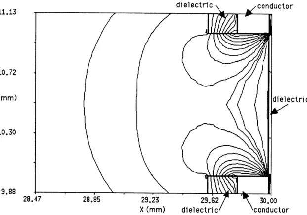
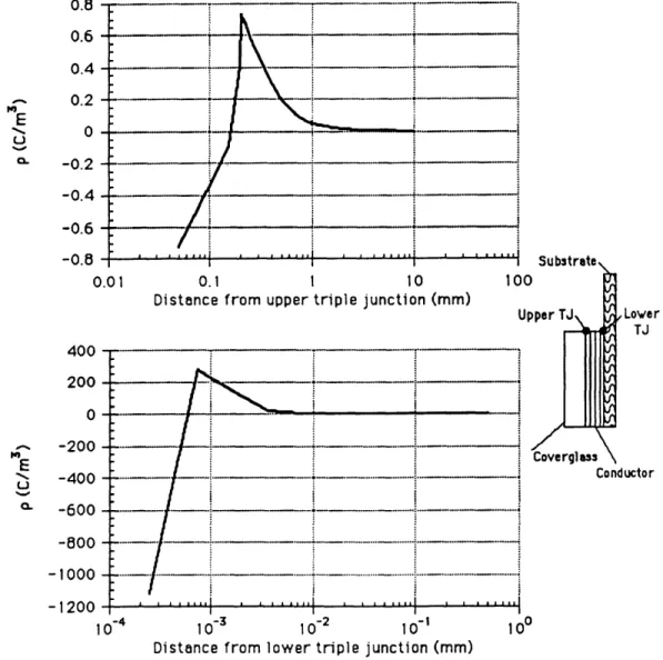
are represented by the electric potential plot (Fig. 2.3) and the surface charge density plot (Fig. 2.4). Corresponding plots for the WTC geometry are shown in Figs. 2.12 and 2.13. As expected, the highest potential value is on the conductor surface with gradients falling off quickly around this voltage source. The gap is sufficiently large that the gradients do not interfere but rather connect at the coverglass surface. The potential lines fall off uniformly beyond the coverglass surface. Above the substrate surface, the potential gradients concentrate near the conductor with potential lines peaking sharply in the center due to the grid configuration. In the coverglass, the potential gradients are curved near the edge of the cell but straighten away from the cell edge.
To simulate the electric field build up, the modified PIC code is run with the enhanced electron field emission (EFEE) charging processes included. The initial conditions are obtained from the results of the ambient ion charging calculations and the enhancement factor, 3, for each conductor cell. Due to the high electric potential normal to the conductor surface, much lower enhancement factors (p 1 30-60) are used to reduce the number of electrons emitted from the conductor. When too many electrons are emitted, the EFEE charging time is too small, making it less than or on the order of a capacitor charging time. The timestep also affects the number of particles injected into the domain,
Di electric
ctric- j: .*: Conductor
Triple Junctions
.. .' a ft!
0.0
Figure 2.11: Typical grid structure for calculations
Diel 21.0 14.0 7.0 30.0 15.0 22.5
dielectric 11.13 10.72 v (mm) dielectric 10.30 9.88 28.47 28.85 29.23 29.62 30.00 X (mm) dielectric conductor
Figure 2.12: Typical electric potential for ambient ion charging of WTC cells
so it is typically chosen to be w, At = 0.01. Larger timesteps can be used when fewer particles are in the domain, which occurs when the electric field at the triple junction has not increased enough for EFEE charging to begin. The PIC code is run until the electric field runs away at one or both of the triple junctions. Since the PIC code automatically accounts for space charge effects, the simulation is often run beyond the electric field runaway into the space charge current limited regime, which limits the electric field magnitude.
The cell properties used for the WTC simulations are based on the Space Station Freedom WTC cell. The coverglass and semiconductor are each 203,im (8 mil) thick, and the cell gap is Imm. The semiconductor is silicon, which has a work function of 4.85eV. The coverglass is assumed to be ceria-doped microsheet (CMX) with a dielectric constant of 4 and secondary electron properties of Ema, = 400V and m,, = 4. The Kapton
substrate has a dielectric constant of 3.5 and assumed secondary electron properties of
EI = 300V and r = 3.
The EFEE charging of the WTC cells over the range of 300-500V is distinguished by two classes of behavior, the first occurring with lower 3 (-30) values and the second occurring with higher 3 (-50-60) values. As seen in Figs. 2.14 and 2.15, the electric
0.1 1 10 Distance from upper triple junction (mm)
100 Upper
100 Distance from lower triple junction (mm)
Figure 2.13: Typical surface charge density along the side dielectric surface after ambient ion charging of WTC cells 0.8 -0.6 -0.4 - 0.2- 0--0.2 ---0.4 --0.6 --0.8 0.01 E U M E a-%. tJ (2. 400 200 0 -200 -400 -600 -800 -1000 -1200 - - - -. ... i... . ... . .. ... . .. i i ~ l * i ' t l 1 i i l i . l l l i 10- 4 10-3 10-1
3.0 10 - 2.8 10 s ... ... ... .... .. ... ... S2.4 10 I-22 10 . 22 10s ... .... .... ... ... 2.20 1.6 10 1.4 105 0.0 100 4.0 10's 8.0 10s 1.2 104 time (sec)
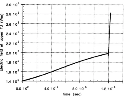
Figure 2.14: Class 1 electric field at upper triple junction versus time
field at the upper triple junction increases initially for the first class and decreases initially for the second class. No runaway occurs at the lower triple junction within this time.
In the first class, the ambient ion charging continues to build up the electric field at the upper triple junction until it is high enough to initiate EFEE charging. Once initiated, the high flux of electrons causes the field to decrease for a short time before the runaway. As shown in Fig. 2.16, the surface charge along the side of the coverglass does not change much during the ambient ion charging, as expected, but also does not change much during the electric field runaway. The surface charge along the front surface, however, does increase substantially, indicating that the electrons from the conductor are striking there and increasing the surface charge through secondary electron emission.
In the second class of behavior EFEE charging begins immediately, emitting many electrons into the domain. Although the surface charge density does increase, as shown in Fig. 2.17, most of the electrons quickly exit the domain without striking any of the cell surfaces. Just prior to runaway, the difference between the number of electrons emitted and the number of electrons impacting the dielectric increases substantially at the same time that the total number of electrons in the domain increases substantially. The electric field then runs away, and the surface charge density along the coverglass side and front surfaces increases significantly.
4.5 10 s 4.0 10s I- . ... ... --. 3.0 10 .CL S s ... ... . ... .... ... 2.510 S 2.0 10s ... S 1.5 10 1.0 10 5.0 10 0.0 100 5.010 -8 1.0 10 7 1.51077 2.010- 7 2.510-7 time (sec)
0 -.. 0.1 --0.2 --0.3 -. -0.4 -. -0.5 -. -0.6 --0.7 -. -0.8 0.04 100- 10- 1- 0.1- 0.01-0.UU I 0.06 0.08 0.1 0.12 0.14 0.16
Distance from upper TJ (mm) (a) Coverglass side surface
... ... Am bient ion charging -0-- Initial EFEE charging ... ... ... -- Before runaw ay
-- - During runaway
I- I-- I---- I---
---4 6 8
Distance from upper TJ (mm)
10 12
10 12
(b) Coverglass front surface
Figure 2.16: Class 1 surface charge density over the coverglass (a) side surface, (b) front surface
. . . .