Publisher’s version / Version de l'éditeur:
Vous avez des questions? Nous pouvons vous aider. Pour communiquer directement avec un auteur, consultez la première page de la revue dans laquelle son article a été publié afin de trouver ses coordonnées. Si vous n’arrivez pas à les repérer, communiquez avec nous à [email protected].
Questions? Contact the NRC Publications Archive team at
[email protected]. If you wish to email the authors directly, please see the first page of the publication for their contact information.
https://publications-cnrc.canada.ca/fra/droits
L’accès à ce site Web et l’utilisation de son contenu sont assujettis aux conditions présentées dans le site LISEZ CES CONDITIONS ATTENTIVEMENT AVANT D’UTILISER CE SITE WEB.
Physica Status Solidi: Rapid Research Letters, 3, 6, pp. 199-201, 2009-06-02
READ THESE TERMS AND CONDITIONS CAREFULLY BEFORE USING THIS WEBSITE.
https://nrc-publications.canada.ca/eng/copyright
NRC Publications Archive Record / Notice des Archives des publications du CNRC : https://nrc-publications.canada.ca/eng/view/object/?id=e8172abc-03ff-4a20-b41f-80c8519ce0db https://publications-cnrc.canada.ca/fra/voir/objet/?id=e8172abc-03ff-4a20-b41f-80c8519ce0db
NRC Publications Archive
Archives des publications du CNRC
This publication could be one of several versions: author’s original, accepted manuscript or the publisher’s version. / La version de cette publication peut être l’une des suivantes : la version prépublication de l’auteur, la version acceptée du manuscrit ou la version de l’éditeur.
For the publisher’s version, please access the DOI link below./ Pour consulter la version de l’éditeur, utilisez le lien DOI ci-dessous.
https://doi.org/10.1002/pssr.200903121
Access and use of this website and the material on it are subject to the Terms and Conditions set forth at
Two modes of electroluminescence from single-walled carbon
nanotubes
p s s
reprints
status
solidi
www.interscience.wiley.com
physica
REPRINT
www.pss-rrl.com
www.pss-c.com
www.pss-b.com
www.pss-a.com
© 2009 WILEY-VCH Verlag GmbH & Co. KGaA, Weinheim
www.pss-rapid.com
pss
Phys. Status Solidi RRL 3, No. 6 , 199– 201 (2009) / DOI 10.1002/pssr.200903121
Two modes of electroluminescence
from single-walled carbon nanotubes
Jacques Lefebvre*, 1
, D. Guy Austing1
, and Paul Finnie1
Institute for Microstructural Sciences, National Research Council, Ottawa (Ontario), K1A 0R6, Canada Received 1 May 2009, revised 27 May 2009, accepted 28 May 2009
Published online 2 June 2009 PACS 78.60.Fi, 78.67.Ch
* Corresponding author: e-mail [email protected]
© 2009 WILEY-VCH Verlag GmbH & Co. KGaA, Weinheim
1 Introduction Light emission from single-walled
carbon nanotubes (SWNTs) is now routinely observed, in particular for the photo-excitation, but also for electro-excitation of charge carriers (for a recent review, see Ref. [1]). Indeed, photoluminescence (PL) is a mainstay of SWNT characterization. Properly prepared SWNTs have sharp PL peaks (~ 10 meV at room temperature) with nar-row linewidths and excellent quantum yield [2–4]. On the other hand, electroluminescence (EL) remains less well developed, with experimental challenges including more difficult sample preparation, and the need to combine optical and electronic setups. In contrast to PL, EL reveals a spectrally broad emission with low quantum yield [5–10].
The best PL spectral properties are obtained when the SWNTs are minimally perturbed, as in, for example, as-grown air-suspended SWNTs. However, for EL meas-urements, SWNTs typically undergo several processing steps which are potential sources of defects or contami-nation leading to non-radiative decay channels. In this let-ter, we report the spectrally resolved EL signal from sam-ples free from post-growth processing. We find that while most SWNTs emit over a broad range (roughly 1200 nm to 1650 nm), a small number emit sharply peaked EL (< 50 nm bandwidth). Moreover, the onset of sharp EL oc-curs at lower bias than the broad EL. The narrow EL is analogous to PL, and is a signature of the SWNT band structure. In contrast, the broad EL is non-specific, but
rather, likely a common feature of almost any material brought to high temperature.
2 Results and discussion The samples, 1 cm2
scale pieces of SiO2 (1 µm thick) on Si (500 µm thick), were
patterned by photolithography to produce large Pt contact electrodes. E-beam evaporated Co thin film (< 1 nm thick) was also patterned to provide catalyst areas for chemical vapour deposition (CVD) using ethanol as the carbon source [11]. Importantly, CVD is the last stage of the de-vice fabrication, therefore preserving, as much as possible, the pristine nature of the nanotubes. Platinum was used for the electrodes because of its compatibility with the high CVD temperature.
Figure 1a shows a sample with several nanotubes bridging a ~ 4 µm gap between source and drain electrodes. The vast majority of nanotubes in this sample are in imme-diate contact with the SiO2 substrate. EL measurements
were performed on a probe station equipped with an InGaAs camera (sensitivity between 900 – 1650 nm, inte-gration time 1 – 2 s) to detect light emission. Several nano-tubes bridged the gap between source and drain, leading to several parallel nanotube channels which simultaneously emitted EL. An image of the EL from the gap area is shown in Fig. 1b. The source – drain voltage was typically between 8 V and 10 V while the source – drain current was several hundred µA. Under these conditions, the current was observed to saturate (i.e. the current showed little in-
The electroluminescence from single-walled carbon nanotube field effect transistors is spectrally resolved, and shows two distinct modes of light emission. The vast majority of nano-tubes have spectrally broad emission consistent with the spec-trum of blackbody radiation. Much more rarely, superposed
on the broad emission is a single narrow (< 50 meV) peak which is consistent with expectation for electron – hole re-combination. The narrow emission is strong even at lower bi-ases and in general has greater peak intensity than the broad-band emission.
200 J. Lefebvre et al.: Two modes of electroluminescence from single-walled carbon nanotubes
© 2009 WILEY-VCH Verlag GmbH & Co. KGaA, Weinheim www.pss-rapid.com
status solidi
physica
rrl
Figure 1 (online colour at: www.pss-rapid.com) a) Scanning electron micrograph (SEM) of an array of single-walled carbon nanotubes on SiO2 between platinum electrodes. b) Electrolumi-nescence (EL) image of a similar region. The background emis-sion surrounding the electrodes arises from a low level of white light illumination. The SEM and EL images are from different devices. The scale bars are 10 µm.
crease with increased bias) as transport is limited by scat-tering by optical phonons [12, 13]. With a typical satura-tion current of 20 µA per nanotube, we estimate that 10 to 20 nanotubes in parallel dominated the transport in our samples, which is consistent with the number of EL spots in a given image. This is the case in Fig. 1b with 10 – 15 spots over the entire 50 µm length of the gap. The gate voltage dependence of the EL signal was not system-atically studied here, but sweeping the gate had little effect on the EL (the gate voltage was generally set to zero with respect to the drain electrode).
An important observation is that for the highest bias of 10 V, some emission spots suddenly disappeared and oth-ers appeared, with the eventual end state of an open circuit. Current carrying SWNTs reach high enough temperatures to readily oxidize in air [14]. Current must then travel through other remaining nanotubes in the conductive net-work, producing new emission spots. Although changes in oxide trap configuration could also produce similar fluc-tuations, they would not lead to irreversible device failure.
The main result of this work is demonstrated in spa-tially and spectrally resolved EL images (Figs. 2 and 3). Following Ref. [11], the line of emission spots in Fig. 1b is equivalent to a slit in a grating spectrometer. Spectral im-aging is readily achieved by placing a diffraction grating in the light path to the camera. In Fig. 2, purely spatial im-ages of the EL are shown in the left column. In the right-hand column of Fig. 2, the horizontal axis is spectrally re-solved (wavelength in nm) while the vertical is spatially resolved.
The emission spectra were taken at increasing source – drain voltage starting at 4 V bias for a) and increasing in steps through b) and c) to 8 V in d). The precise bias volt-age for b) and c) was not recorded. At the low voltvolt-ages, the spectrum is dominated by a single, narrow emission peak (Fig. 2a – b), with a linewidth of 40 nm (35 meV). At higher voltages (Fig. 2c – d), broad and featureless emis-sion peaks appear extending from 1250 nm to wavelengths
Figure 2 (online colour at: www.pss-rapid.com) Electrolumi-nescence from single-walled carbon nanotubes. a) Imaging spec-trum showing a single narrow emission peak at 1600 nm. The vertical axis is spatially resolved; the horizontal axis is spectrally resolved. b) The same scan, but at higher bias. The corresponding purely spatially resolved image (x and y) is shown to the left (20 µm scale bar). c) – d) The same scans at still higher biases. The bias was increased in steps from a minimum 4 V in a) to a maximum 8 V in d).
beyond the detector cut-off of 1650 nm. This broad emis-sion is the spectral signature of the majority of EL spots, similar to previous reports [6, 8]. The narrow emission is still visible at higher voltages and does not broaden signifi-cantly.
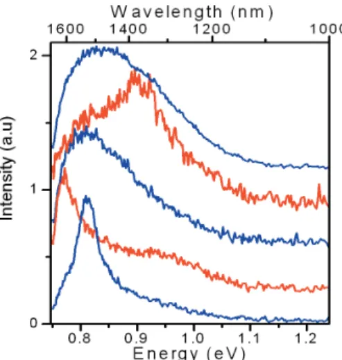
Figure 3 shows several spectral slices taken from EL imaging spectra like Fig. 2. Of the five different spectra shown, two are essentially broadband and featureless while three show peaks of various relative intensity. The narrow-
Figure 3 (online colour at: www.pss-rapid.com) Examples of electroluminescence spectra from different single-walled carbon nanotubes. Virtually all cases show broad long wavelength emis-sion. A few cases show sharp emission peaks.
Phys. Status Solidi RRL 3, No. 6 (2009) 201
www.pss-rapid.com © 2009 WILEY-VCH Verlag GmbH & Co. KGaA, Weinheim
Rapid Research Letter
est emission peak in Fig. 3 has a 35 meV linewidth, a value significantly lower than the 80 – 100 meV reported thus far [9, 10].
Consistent with Ref. [8], the broad emission can be ex-plained by blackbody radiation. Using Planck’s radiation theory, a 2 µm segment of a 1 nm diameter nanotube emits 2 × 10⁵ photons/s at 600 °C (or 25 fW) at 1600 nm (over a 2.5 nm spectral bandwidth). This number is well above the detection limit of the camera and blackbody radiation is detectable in SWNTs even at relatively modest tem-peratures. Assuming that at high bias the EL spots are in-deed disappearing due to oxidation in air [14], it is well es-tablished from thermogravimetric analysis (TGA) that SWNTs burn between 500 °C to 700 °C [15]. This is con-sistent with the conclusion that here SWNTs are reaching such temperatures.
The narrow EL becomes visible at much lower source– drain bias (a third or a half of the breakdown voltage) where the nanotube temperature should be closer to room temperature and the blackbody radiation relatively insig-nificant [14]. The fact that the EL linewidth is narrow, and that it is observed at low bias for which blackbody radia-tion is much weaker, suggests that the EL likely arises from excitonic recombination, as is the case for PL.
Even at low biases, the EL linewidths (~ 35 meV) measured are still significantly larger than for a pristine air-suspended nanotube PL (~ 10 meV) [16]. This might be expected on the basis that PL linewidths increase linearly with temperature [17], and that nanotubes reach tempe-ratures from 400 °C to 600 °C in the current EL meas-urements. The PL from SWNTs remains strong but is broad in this temperature range [18]. However, we cannot rule out other mechanisms of broadening. Even at room temperature, surfactant suspended nanotubes can exhibit similarly broad PL linewidth. Contact or proximity of a nanotube to surfaces can shorten the PL lifetime. More importantly, PL linewidths are generally measured in the linear excitation regime (emission intensity is linear with excitation intensity), implying low densities of photo-excited electrons, holes and excitons. However, we were only able to detect EL at high injection currents (of order 10 µA per nanotube). For reference, 1 µA corresponds to 6 × 10¹² electrons/s. A rough estimation of EL intensity in-dicates that typically 105– 107 photons/s are emitted. Thus for each EL emitting exciton, there are 105– 107 electrons (or holes) present. Therefore the linewidth is expected to be increased as a result of Auger processes which reduce the exciton lifetime.
The relative rarity of the narrow EL compared to broad EL may mean that narrow EL nanotubes might have local potential barriers favourable for EL to occur, for example at a locally suspended segment (a situation similar to Ref. [6]). It may be that a suitable barrier could be created at a nanotube/nanotube junction in such a network, the bot-
tom nanotube acting to reduce the interaction of the top nanotube with the substrate, or producing a discontinuity favouring exciton recombination.
3 Conclusion This work demonstrates that EL in
SWNTs can arise in two spectrally distinct modes, each of which must originate from its own distinct mechanism. The broad, featureless EL is essentially blackbody radia-tion and occurs when devices are driven to sufficiently high currents that the nanotubes are Joule heated. The sharply peaked EL appears to be the electrically excited analog to PL. Only a handful of nanotubes out of many in a device show narrow EL. We have yet to determine the spe-cific conditions which favour narrow EL over broad EL. The higher peak intensity and lower threshold for EL sug-gest that the narrow EL has greater promise for SWNT based optoelectronics.
Acknowledgements The authors are grateful to IMS staff for the fabrication and characterization of samples, particularly H. Tran, P. Marshall, and P. Chow-Chong.
References
[1] A. Jorio, G. Dresselhaus, and M. S. Dresselhaus (eds.), Car-bon nanotubes: Advanced topics in the synthesis, structure, properties and applications, Topics in Applied Physics, Vol. 111 (Springer-Verlag, Berlin, 2008).
[2] M. J. O’Connell et al., Science 297, 593 (2002).
[3] J. Lefebvre, Y. Homma, and P. Finnie, Phys. Rev. Lett. 90, 217401 (2003).
[4] S.-Y. Ju, W. P. Kopcha, and F. Papadimitrakopoulos, Sci-ence 323, 1119 (2009).
[5] J. A. Misewich, R. Martel, Ph. Avouris, J. C. Tsang, S. Heinze, and J. Tersoff, Science 300, 783 (2003).
[6] J. Chen, V. Perebeinos, M. Freitag, J. Tsang, Q. Fu, J. Liu, and Ph. Avouris, Science 310, 1171 (2004).
[7] L. Marty, E. Adam, L. Albert, R. Doyon, D. Ménard, and R. Martel, Phys. Rev. Lett. 96, 136803 (2006).
[8] D. Mann et al., Nature Nanotechnol. 2, 33 (2007). [9] E. Adam et al., Nano Lett. 8, 2351 (2008). [10] L. Xie et al., Nano Lett. 9, 1747 (2009). [11] J. Lefebvre et al., Nano Lett. 6, 1603 (2006).
[12] Z. Yao, C. L. Kane, and C. Dekker, Phys. Rev. Lett. 84, 2941 (2000).
[13] E. Pop, D. Mann, J. Cao, Q. Wang, K. Goodson, and H. Dai, Phys. Rev. Lett. 95, 155505 (2005).
[14] E. Pop, D. Mann, K. Goodson, and H. Dai, J. Appl. Phys. 101, 093710 (2007).
[15] J. P. C. Trigueiro et al., J. Nanosci. Nanotechnol. 7, 3477 (2007).
[16] J. Lefebvre, J. M. Fraser, P. Finnie, and Y. Homma, Phys. Rev. B 69, 075403 (2004).
[17] J. Lefebvre, P. Finnie, and Y. Homma, Phys. Rev. B 70, 045419 (2004).
[18] P. Finnie, Y. Homma, and J. Lefebvre, Phys. Rev. Lett. 74, 247401 (2005).