An Application of Lean Principles within a Semiconductor Manufacturing Environment
By
Roy C. Wildeman, Jr.
Bachelors of Arts in the Engineering Sciences, Dartmouth College (1999) Bachelors of Engineering, Thayer School of Engineering at Dartmouth College (1999)
Submitted to the Department of Mechanical Engineering and the Sloan School of Management
in Partial Fulfillment of the Requirements for the Degrees of Master of Business Administration
Master of Science in Mechanical Engineering
In Conjunction with the Leaders for Manufacturing Program at the Massachusetts Institute of Technology
February 2005
C2005 Massachusetts Institute of Technology. All rights reserved.
Signature of Author
January 14, 2005
MIT Sloan School of Management Department of Mechanical Engineering
Certified by
Stephen Graves, Thesis Advisor Abraham J. Siegel Professor of Management Certified by
Dari1W* ey, Thesis Advisor
Senior Lecturer, MIT Engineering Systems Division
Accepted by FA
Margaret Andrews Executive Director of Masters Program Sloan School of Management
Accepted by______________ __________
Acceped byLallit
Anand MASSAUfl-_ INSTlTTE Chairman, Committee on Graduate Studies
O - - Department of Mechanical Engineering
An Application of Lean Principles within a
Semiconductor Manufacturing Environment
By
Roy C. Wildeman, Jr.
Submitted to the Sloan School of Management and the Department of Mechanical Engineering on January 14, 2005 in partial fulfillment of the Requirements for the Degrees of Master of Business Administration and Master of Science in Mechanical Engineering
Abstract
Intel Corporation's Fab 23 is committed to implementing lean manufacturing to reduce their production cycle times and cost. This thesis is focused around the development of the principles of lean that are most relevant to Intel's complex manufacturing flow and then the application of these principles to improve the operations in a focused area, the Sorting floor. Direct examination of the work in Sort raises the awareness of
inefficiencies from overproduction and inventory; viewing this work as a series of structured activities, customer-supplier connections, and simplified flows further crystallizes the need for a structured approach towards WIP management. A pilot
implementation of a CONWIP control of inventory demonstrates reductions in cycle time variability and provides a foundation for further improvements. In conclusion, the
challenges experienced with changing the manufacturing systems in Sort were largely organizational and likely to be seen in many other operational areas at Fab 23.
Thesis Supervisor: Stephen Graves
Title: Abraham J. Siegel Professor of Management Thesis Supervisor: Daniel Whitney
Acknowledgements
I would like to thank the Intel Corporation for its support of the Leaders for
Manufacturing Program at MIT. By structuring a challenging internship and then providing me with the resources to succeed, Intel has contributed incredibly to my educational experience. A long list of individuals deserve my thanks. A few on the list include: Jim Beuerle, Rob Garber, John Grad, Gary Barbari, Blane Volkmer, Martin Huebschman, Marion Shumway, and John Sheridan. The Operation Managers and Technicians within the Sort area were also instrumental in the project's success - thank you Lynn Yarmer, Chris Vigil, Chris Curl, Pam Usher, Darlene Santistevan, Joe Phillips, Donna Jones, Reuben Sanchez, Joe Wagner, Clint Thielemier, and all the people in Sort for trying something new. Lastly, I owe a great thanks to Morgan Burke, Allan Rowe, Clay Carlson, and Jamie Flinchbaugh for always challenging my understanding of lean and its application to semiconductor manufacturing.
I wish to also thank all the directors, staff, faculty, and students of the Leaders for Manufacturing Program at MIT. I am particularly grateful for the council of Steve Graves, Dan Whitney, and Jan Klein. Their ceaseless questions, support, and guidance helped create structure and direction for this thesis project.
Lastly, I thank my family for all their support and encouragement and my wife Pam for her love and patience.
Table of Contents
1. IN TR O D U C TIO N ... 9
1. 1 THESIS STRUCTURE ... 9
2. BU SIN ESS BA CK G R O U ND ... 11
2.1 FAB 23 H ISTORY ... 11
2.2 BUSINESS ENVIRONM ENT ... ,... 11
2.3 K EY TAKEAW AYS... 12
3. OVERVIEW OF MANUFACTURING EXCELLENCE (MX) ... 13
3.1 TECHNICAL GOAL... 13
3.2 CULTURAL G OAL ... 13
3.3 IM PLEM ENTATION STRATEGY ... 14
3.3.1 Lean Rules & Principles (not Tools)... 14
3.3.2 Pulling in Change on two fronts: "Mile- Wide, Inch-Deep" and "Inch-Wide, Mile-Deep" ... 15
3.4 THESIS FoCUs... 16
4. FLA SH M EM O R Y SO R TIN G O PER A TION S ... 17
4.1 SORT PROCESSING ... 17
4.1.1 Process Technology P803 ... 18
4.1.2 Process Technology P804 ... 19
4.1.3 The Product M ix of P803 and P804 Processing ... 19
4.1.4 Lot H andling & Changeovers ... 19
4.2 O RGANIZATIONAL STRUCTURE... 20
4.3 SORT ECONOM ICS & M ETRICS... 21
4.4 K EY TAKEAW AYS ... 22
5. DIRECT OBSERVATION OF THE CURRENT REALITY... 23
5.1 A CTIVITY M APPING ... 23
5.2 PRODUCT/PROCESS M APPING ... 24
5.3 V ARIABILITY IN CYCLE TIM ES... 24
5.4 TESTER U TILIZATIONS ... 28
5.5 REW ORK RATES... 29
5.6 FAB 23 PLANNING AND PRODUCT D ELIVERY TO SORT 23 ... 30
5.7 PRODUCTION SCHEDULING D YNAM ICS... 32
5.8 CAPACITY M ANAGEM ENT SYSTEM S ... 37
5.9 W IP M ANAGEM ENT POLICIES... 38
5.10 K EY TAKEAW AYS ... 39
6. HYPOTHESES FOR CHANGE TOWARDS THE IDEAL STATE ... 41
6.1 MX RULE #1: STRUCTURE EVERY ACTIVITY ... 42
6.2 MX RULE #2: CLEARLY CONNECT EVERY CUSTOMER-SUPPLIER RELATIONSHIP... 43
6.3 M X RULE #3: SPECIFY AND SIMPLIFY EVERY FLOW ... 45
6.4 K EY TAKEAW AYS... 46
7. EX PER IM EN TA TIO N & IM PLEM EN TATIO N ... 47
7.1 MX RULE #4: IMPROVE THROUGH EXPERIMENTATION AT THE POINT OF ACTIVITY ... ,... 47
7.2 CLEAR INSTRUCTIONS AND EXPECTATIONS FOR THE CHANGE... 47
7.3 RESULTS VERSUS EXPECTATIONS ... 50
7.4 LEARNINGS AND REFINEM ENT ... 55
7.5 K EY TAKEAW AYS ... 55
8.1 O RGANIZATIONAL D ESIGN ... 57
8.1.1 Organizational Structure ... 57
8.1.2 Job D esign of the M anufacturing Technicians... 58
8.2 THE INTEL CULTURE... 58
8.2.1 The D ifferent Sym bols of mX at Fab 23 ... 58
8.2.2 The fit of mX within the Intel's Values ... 59
8.3 CONCLUSIONS... 61
9. TER M S A ND A C R O NY M S... 62
1. INTRODUCTION
Increasingly, American companies are off-shoring their manufacturing operations - a trend which creates an uncertain economic climate domestically alongside lots of political controversy. Amid the shakeup of globalization, one thing seems certain: operations that are plagued with inefficiencies can and will continue to be replaced by those which are more nimble and efficient across an international playing field. To remain competitive in the years ahead, many manufacturers must recognize their competitive reality and continually seek to remove the waste that has accumulated in their processes. In many ways, this thesis research is a story about one such entity
-Intel's Fab 231 in Colorado Springs, Colorado. In benchmarking other world-class
manufacturing systems, Fab 23 is attempting to leverage principles of lean manufacturing towards a greater competitive advantage that will sustain their long-term survival in an increasingly competitive world.
Many pundits question the applicability of lean to the kind of complexity found within a semiconductor production line. In response, this thesis is centered on Fab 23's
interpretation of the principles of lean - that is, fundamental laws that govern process excellence - and the general applicability of these principles through a targeted study of the facility's sorting operations. By experimenting with lean thinking in Sort, this research provides a deeper understanding of the types of continuous learning, benefits, and barriers that are unique to a lean initiative within a semiconductor environment.
1.1 Thesis Structure
A brief overview of the thesis structure is as follows:
Chapter 2 describes the history of Fab 23, the current business climate for flash memory, and summarizes the strategic operational goals the fab needs to achieve in order to remain competitive in the future.
Chapter 3 provides an overview of the lean initiative at the fab, called Manufacturing Excellence (or mX). The principles of mX will be described in detail along with a summary rationale for focusing this research on the facility's sorting operations. Chapter 4 is an overview of the Sort 23 operations, including the high-level process
flows, management structure, and economic drivers of the group.
Chapter 5 is a deeper study into the operating characteristics and latent wastes within the sort production process. Both direct observation and statistical analyses are used to gauge the level and severity of these different wastes while creating tension for change.
Chapter 6 presents several specific hypotheses for change towards Sort's ideal state. Each opportunity is viewed through the lens of the mX rules i.e. seeing work as a series of
structured activities, customer-supplier relationships, and simplified flows that can be continually improved upon towards the ideal state.
Chapter 7 describes the methodology and results from an implementation of one of these aforementioned opportunities, namely a CONWIP control of inventory to promote more consistent and streamlined cycle times across Sort's product flows.
Chapter 8 highlights some of the key challenges experienced with changing the
manufacturing systems in Sort. The research concludes that many of the barriers to mX remain largely organizational and are likely to be seen in many other operational areas at Fab 23.
2. BUSINESS BACKGROUND
"I think it's safe to say we're emerging from the worst IT/telecom recession in our
lifetime. Ahead of us are a set of opportunities unparalleled in our past."'
-Intel Capital President John Miner (Fackler, May 2004)
2.1 Fab 23 History
Fab 23 in Colorado Springs is Intel's sole manufacturing source for a mature flash memory technology. Flash memory chips retain memory even when a device is shut off, and they are commonly used in cell phones, digital cameras, and PDAs. Originally, Intel purchased the factory from the Rockwell International Corporation in February of 2000 to rapidly add more manufacturing capacity in support of the booming demand for Intel products (Intel, June 2004). Representing an investment of $1.5 billion to manufacture not only flash memory but also logic devices, Fab 23 quickly set a new Intel record for the fastest start up for a 200mm manufacturing site. In support of this rapid ramp, the Fab
23 employee base was expected to grow over 1,000 as the factory became fully loaded.
With the unexpected technology recession in late 2000, Fab 23 was suddenly facing a radical change in external environment. In response to the market downturn, the fab embarked on a cost-cutting campaign, dubbed PnL (for Profit and Loss), to coordinate and align functional departments towards operating the factory as an autonomous business entity within Intel's Fab and Sort Manufacturing (FSM) division. By internally focusing on their cost accounting practices, management at Fab 23 was able to drive more business-centric thinking across its organization, focus efforts on controllable cash flow as a ballast against their fixed depreciation stream, and ultimately drive their cash cost per 3K wafer start 2 down 40% over a period of 14 months. The PnL initiative was a major factor in enabling the fab to remain viable as a single-technology supplier during
the economic recession. Significantly, the period was also noted for many lay-offs, infrastructure shut-downs, and other painful spending cuts felt across both Fab 23 and other Intel facilities.
2.2 Business Environment
The semiconductor industry has been steadily recovering over the last two years; the three-month average of worldwide chip sales rose to $16.94 billion in April, 2004 -the highest monthly level since January 2000 -and a growth of 36.6% from the previous year
(Andrey and Greenagel, June 2004). The demand for flash memory has been strong as well, with 2003 sales volumes up almost 27% from the previous year (Kanellos, November 2003).
The overall flash market is divided into two main technologies: NAND (for
"NOT-AND" -a reference to how data is retrieved) and NOR ("NOT- OR"). Intel, Advanced
2 A cost accounting metric used across Intel's Fab Sort Manufacturing division. 3K Wafer Start is a
Micro Devices, and Fujitsu produce primarily NOR flash devices, which have lower density, lower writing speed, and higher reading speeds. NOR devices are also less prone to data corruption and are typically used to store information on cell phones, PDA's, and set-top boxes (Kanellos, November 2003). Reciprocally, Samsung and Toshiba together control about 90 percent of the $4.7 billion market for NAND devices, which can hold more data than NOR, are cheaper at comparable densities, have a higher writing speeds but slower reading speed, and are commonly used in digital camera flash cards and MP3 players (Yoon and Sorid, May 2004).
NAND is the faster growing technology, reaching 40 percent of the overall flash market
from its level of 10% two years ago ("Memory", March 2004). The shift corresponds to a stronger relative demand for digital cameras and MP3 players and has resulted in a turnover in market leadership; Intel had previously led the flash memory market with its focus on NOR technology for over a decade but, in the third quarter of 2003, Samsung, Toshiba, and Spansion (a recent joint venture between ADM and Fujitsu) all overtook the former number one as Intel's market share dropped from 26.1% in 2002 to 13.5% market share at the end of 2003 (Kanellos, November 2003).
Historically, scarce fab capacity worldwide has fueled high margins for the major players in both groups of technology. However, in the spring of 2004 Samsung & Toshiba began slashing their prices to undermine the threat of emerging rivals (Yoon and Sorid, May 2004). Additionally, benchmarking studies revealed Intel flash memory manufacturing lagged all the high-volume manufacturers across both NAND and NOR technologies in terms of cycle time, measured by manufacturing days per mask layer. The relative growth of NAND technology, the aggressive build-up of production capacity by established players, and the potential entry of new players into the NOR technology space all prove to be threats to Intel's margins and share of the flash memory market space.
2.3 Key Takeaways
As a single-technology fab currently producing only a mature NOR technology, Fab 23 must focus on improvements in both cost and cycle time to strategically bolster its
competitiveness among both incumbent and new entrant flash memory manufacturers. Additionally, the fab has a production commitment from Intel to manufacture an added communications technology in the near future. In order to compete in this new market, cycle time reductions are extremely critical, as customers in the communications market are likely to demand radically lower lead times than Intel has traditionally been asked to deliver.
Lean manufacturing is a well-established improvement methodology which emphasizes both waste elimination and speed - a good match with Fab 23's strategic objectives of lower cost and faster cycle times. Next, we will cover the nature of lean at Fab 23, characterized by the Manufacturing Excellence (mX) initiative.
3. OVERVIEW OF MANUFACTURING EXCELLENCE (mX)
"Compete Externally & Lead Internally"
-Recurring communication at Fab 23
In early 2003, Fab 23 collaborated with an internal benchmarking group to explore lean manufacturing as a method to not only capture the common thinking and language that made their recent PnL initiative a success but also drive new improvements in cost and manufacturing cycle time. By emphasizing openness to experimentation and internal
leadership towards operations excellence, Fab 23 strives to ultimately enable Intel's Fab
and Sort Manufacturing (FSM) division to compete externally in the flash memory market. The evolving lean initiative is dubbed Manufacturing Excellence, or mX, and promotes change along both technical and organizational fronts.
3.1 Technical Goal
The primary technical goal of mX is to understand how 'pull' methodologies can be used to improve the cycle times of their complex operating flow. Most generally, a pull system prevents inventory from growing beyond a specified limit by limiting the release of work into particular segments of a process (Hopp and Spearman, Spring 2004, p. 147). The benefits of such disciplined flow are well documented and typically include:
1.) A means to reduce WIP and corresponding cycle time
2.) Smoother production flows for more predicable output
3.) Improved product quality with faster line velocity and a built-in intolerance for
scrap/rework
4.) Continuous reduction in manufacturing costs through the systematic exposure of latent wastes, or "rocks" (Hopp and Spearman, Spring 2004, p. 137)
Pull methodologies have not been widely adopted in the semiconductor industry for a variety of reasons. First, the re-entry nature of semiconductor processing flow creates a highly-complex environment, where multiple process steps can go through a particular toolset and even multiple toolsets that can process a single step. Secondly, the
characteristic variability in tool availability becomes a key obstacle, as unpredictable downtimes become a significant challenge when attempting to structure the strict inventory levels and deterministic run times intrinsic to traditional pull systems.
3.2 Cultural Goal
The primary cultural goal of mX is to engage Manufacturing Technicians (MTs) towards systematically eradicating the waste that continually burdens their factory jobs. A
cornerstone of successful lean manufacturing systems is allowing workers to display their capabilities in-full through active participation in running and improving their own workshops (Toyotaproductionsys tem.net, July 2004). In order to realize this kind of change on the floor, work standardization and structured experiments must be accepted nonns that enforce coordinated improvements across different shifts.
In the ideal state of mX, every employee at Fab 23 views their daily problems as opportunities for learning and systematic waste reduction. In this vision, everyone also uses root-cause analysis as a normal business practice, and systems-thinking is a proliferating skill across all levels of the organization.
3.3 Implementation Strategy
3.3.1 Lean Rules & Principles (not Tools)
At the start of the initiative, the mX team experienced a few set backs. The creation of an Improvement Suggestion Portal was intended to help engage MT's in promoting waste elimination. However, the tool inadvertently revealed a frustrating scarcity of resources to support the surge in improvement suggestions. Some managers also raised concerns about the addition of a redundant improvement channel which paralleled systems already being used. Additionally, extensive time was invested in a detailed value-stream
mapping effort which ultimately led to common-sense conclusions. Frustrated by a lack of progress, the mX team embraced a different implementation strategy which de-emphasizes lean tools and focuses on a shared way of thinking and learning the key principles inherent in lean manufacturing systems.
Prior research on the Toyota Production System has concluded that the recognition and scientific improvement of work activities, connections, and flows throughout an
organization's processes is an intrinsic strength behind Toyota's operational excellence (Spears and Bowen, 1999, p. 98). With the counsel of the Lean Learning Center in Novi, Michigan, Fab 23 has formalized this research into 4 rules that govern and direct new ways of thinking about opportunities for improvement (Flinchbaugh, August 2004, p. 2):
1. Structure every activity
2. Clearly connect every customer-supplier relationship
3. Specify and simplify every flow
4. Improve through experimentation at the point of activity toward the ideal state Here, the ideal state is defined by delivering exactly what our customer wants -exactly when they want it, at the price they want -with zero waste and everyone safe.
Additionally, the mX team has communicated 5 principles which help provide a common vocabulary, lens, and methodology towards the ongoing coaching and support of all mX opportunities:
1. Directly and deeply observe the work in question to understand the current reality
2. Systematically recognize and eliminate waste
3. Systematically solve problems through the scientific method
4. Establish high agreement on the what and how of the proposed change
5. Promote a learning organization that continuously learns, applies, and reflects on its change
These rules and principles of mX are summarized into a "House of mX" schematic, shown in Figure 3.3.
Figure 3.3: The "House" of Manufacturing Excellence (W) principles.
Ideal
_0 4State
Aply Larn.
towards the ideal X
3.3.2 Pulling in Change on two fronts: "Wide, Inch-Deep" and "Inch-Wide,
Mile-Deep"
In early 2004, the mX initiative was being directed by a core of four managers who devoted a significant portion of their time to coaching the rules and principles of lean. As a means to further proliferate this new way of thinking, the core team organized and trained a set of mX Champions to identify key mX opportunities and drive tactical improvements through the coaching, experimentation, and reflection of mX rules and principles in their home functional areas. By targeting troublesome, ongoing problems with mX thinking, Champions could start to solve thorny issues, credit their lean thinking with the success, and hence generate more interest and demand for further mX thinking among their constituents (Klein, October 2004). This approach encompasses the mX core team's "Mile-wide, Inch Deep" campaign.
In parallel, an "Inch-Wide, Mile Deep" initiative was pursued. In this strategy, a subset of operations within the entire flash memory manufacturing line can be selected as an isolated area for open experimentation and deeper learning about lean. In surveying possible candidates, the facility's Sorting operations were selected as Fab 23's first mX
Learning Lab for several reasons:
- Sort 23 has been consistently rated the best Sort operation within Intel in terms of
This history and confidence for success led to a high willingness to experiment with lean among the Sort 23 personnel.
- Flash Memory Sorting is a relatively simple process flow with only a few re-entry loops. Equipment availability is also very high, and the processing times across operations are consistent. These conditions lend to a favorable, stable
environment in which experiments with WIP management and pull methodologies could be explored.
- The flexibility in micro-contamination regulations and clean-room standards presents significantly lower barriers towards implementing any layout changes, visual controls, or visual flow solutions that may be generated from lean thinking. 3.4 Thesis Focus
At the tactical level, the LFM internship was an opportunity to participate in the Sort Learning Lab to help identify and resolve ongoing problems through the use of mX rules and principles. The methodology for this research work was as follows:
1. The work in Sort was directly observed in order to gain an appreciation and sense
for the type and quantity of waste in the area.
2. The mX rules of structured activities, customer-supplier connections, and simplified flows were applied to target latent inefficiencies and generate new opportunities for improving both cost and cycle time.
3. A tactical experiment targeting one of the key opportunities, WIP control, was
then structured and implemented.
4. The results of the experiment were interpreted for further learning and refinement of the change.
Ideally, this scientific approach towards cost & cycle time improvements could be learned from and replicated to other areas in the Fab/Sort production line at Fab 23 for further mX proliferation.
Before directly embarking on the direct observation of the wastes in Sort, however, a brief overview of both the process complexity of flash memory sorting and the formal organization of the Sort 23 group is important.
4. FLASH MEMORY SORTING OPERATIONS
"Folks usually feel Sort is somewhat simple compared to the fab operations. The reality is very different... and the complexity is always a challenge for us to manage."
-Sort 23 Operating Manager
In order to provide a good context for the research undertaken for the thesis, an overview of the processes, organization, and cost structure of Sort 23 is provided. Hopefully, the reader may also gain some appreciation for the daily complexity that confronts this
Operating Manager! 4.1 Sort Processing
The purpose of a "sort" operation is to separate good and bad wafers and individual die thereon, taking wafers in from upstream fab operations and forwarding them to final manufacturing steps. Sort 23 receives its wafers3 from two upstream fab operations: Fab
23 in Colorado Springs and Fab 11 in Rio Rancho, New Mexico. After processing the
wafers, Sort then delivers the fully-sorted lots to a series of downstream Assembled Die Inventory (ADI) warehouses (which supply Intel's Assembly and Test operations with incoming inventory). Figure 4.1 shows how Sort 23's inputs and outputs fit within a greater context of Intel's flash memory supply chain.
Figure 4.1: Intel's networked flow for P803 & P804 process technologies. Sort 23 receives unsorted wafers from both Fab 23 and Fab 11 for testing & subsequent delivery to an Assembled Die Inventory (ADI).
Fab 23 in Colorado Sort 23
Springs, Colorado - (P803
(P803 Wafers) &P804) Assembly Test
A (Die) -p (Die) C
Fab 11 in Rio Rancho, Sort 11 New Mexico (P804)
(P804 Wafers)
The wafers from both Fab 23 and Fab 11 arrive in lot sizes of 25. Depending on the wafers' upstream origin, Sort must then continue processing these lots through one of two standardized manufacturing processes, referred to as the P803 and P804 process
technologies. In Sort, each of these process technologies is a fixed series of operations that enforce the following responsibilities:
1.) Test and remove wafers with out-of-spec electrical connection properties.
2.) Program memory functionality within each flash memory die.
3.) Stabilize the die's electrical properties and force a failure of any marginal die.
4.) Provide valuable end-of-line data for feedback to upstream operations in the fabs. 3 A wafer is a silicon disc approximately 1 mm thick and 200 mm in diameter. Wafers are used to form the substrate of each flash memory die. Each wafer may produce a quantity of die devices ranging from several hundred to a few thousand, depending on the die product's type and size.
5.) Electronically 'mark' any non-functional die in preparation for the downstream Assembly operations.
Notably, the P03 and P804 process technologies each have a different process flow to handle the unique characteristics of different flash memory designs.
4.1.1 Process Technology P803
Figure 4.1.1 shows the sorting process flow for the P803 technology products. First, all lots are taken through an E-Test process, where the interface structures created between the die during fabrication are tested for functionality. The data gathered at E-Test is compared to nominal process values; out-of-spec material is either immediately scrapped or placed on hold for further investigation depending on the reason for failure.
Figure 4.1.1 Sort Process Flow for P803 Technology
E-Test Pre- Sort 1 Bake Sort 2 Pack &
Bake Ship
Fab 23 Ship to
Delivery ADI
From E-test, the lots move to the first Pre-Bake operation. Bake operations stress marginal die to encourage failure as electrical charge is stabilized within each memory cell.
Thereafter, a lot is brought to the first sorting operation (Sort 1). Sort 23 operates a total of 63 sorting testers which have the flexibility to process any sorting operation (i.e. Sort 1 or Sort 2) on any process technology (P803 or P804). At each of these sort operations, the testing program, or Test Tape, checks that each individual die is functional. Die that fail are classified into bins based on the test which caused them to fail. The bin distribution of die on a wafer is another indicator which can cause material to be put on hold for further investigation by engineering. All sort test results are then loaded into a database system, and non-functional die are mapped in a computerized file that allows downstream
assembly operations to discriminate between die which should be scrapped and die which should be processed further.
After the first Sort operation, an additional Bake operation is required to further stabilize the electrical charges. After the second Bake step, the wafers go through a second sorting operation (Sort 2) which not only checks die functionality but also programs each die with the necessary memory logic.
The final operation, Pack and Ship, prepares the wafers for shipment to the appropriate
4.1.2 Process Technology P804
Figure 4.1.2 shows the sorting process flow for the P804 technology products. Cross-site wafers arrive at Fab 23 ready for processing at the Sort 1 operation. Two subsequent Bake-Sort processing loops are then required to fully stabilize, program, and test die functionality. Again, the same 63 sorting testers have the flexibility to handle any of the
Sort 1, Sort 2A, or Sort 2 operations. The final operation, Pack and Ship, is identical with both the P803 and P804 technologies.
Figure 4.1.2 Sort Process Flow for P804 Technology
Sort 1 Bake Sort 2A Bake Sort 2 Pack &
Ship
Fab 11 Ship to
Delivery ADI
4.1.3 The Product Mix of P803 and P804 Processing
Fab 23 is currently a single-technology fab, supplying Sort with a varying suite of between three to nine products within the P803 process technology. Although Fab 11 manages more than one process technology in their operations, they only supply Sort 23 with between two and three flash memory products from their P804 technology process. Although the product mix can change over time, a larger majority of Sort's throughput volume is for the P803 flash products (approximately 82% of the wafers output during March and April of 2004 were P803). Note that although the throughput volume is smaller for the P804 products, the additional sort operation required for 804 technology leads to nearly 50% of the sorting tester capacity allocated to P804 on any given week. In a way, Sort separates two very different manufacturing environments at Intel. As
Sort's supplier of production material, both wafer fabrication facilities principally
manage their product flow in lots which are segmented by process technology. Intel's Assembly and Test facilities have the most-immediate need for product from the Sorting operation; these customers require delivery of functional die segmented by product to feed their ADI levels. Sort operations then face a weekly challenge of connecting a downstream demand for product-specific die with an upstream supply of process technology-centric wafer lots.
4.1.4 Lot Handling & Changeovers
All wafer lots are loaded and moved between equipment sets manually. To facilitate
manual handling, there are WIP racks nearby each of these processes in order to stage incoming lots.
The E-test and Sort tester operations require that equipment be setup differently for each product type. When a different product is run at these operations, several activities must be performed:
1. The correct software program, or 'Test Tape', must be loaded
2. The unique hardware interface, or probe-card, must be available and installed onto the equipment
3. The tester must be brought to the correct operating temperature.
The product-specific test programs can be substantially different due to programming logic and number of die per wafer, resulting in differing processing times across products. Typically, product changeovers require between 7 and 13 minutes of tester downtime to complete depending on the range and direction of temperature change (heating the tester cell is faster than cooling). Changing a tester to operate on a different process technology is essentially the same as a product-to-product changeover in this regard.
In the case of purely flexing a Sort tester over to a different sorting operation (i.e. from Sort 1 to Sort 2 with no change in product-type), a probe-card change is not required. However, the required temperature change between sorting operations is typically more significant, raising the required tester downtime to between 5 and 45 minutes depending on the direction of the necessary temperature change.
4.2 Organizational Structure
The Sort 23 organization is a relatively small department, consisting of a Department Manager, two Operating Managers who directly manage 4 shifts of Manufacturing Technicians, and two teams of Process and Equipment Engineers (see Figure 4.2). Sort is also supported by several Automation & Industrial Engineering resources who normally work during the daytime-shifts, Monday through Friday.
Figure 4.2: Sort 23 Organization
AllocaEe Prce Fsb/Sort Fboductilon Operating Manager Operatin Manager
(Days & Nights for I' half of (Days & Nights for 2nd hal of
AouWgg0* & Equipment Engineers Process Engineers Shift Shift
ttrw sationSfymorng
Support Staff Manufacturing Technicians Manutacturdng Technicians
Industrial Engineers
The Operating Managers (OMs) split production responsibilities across the first half (front-half) and second half (back-half) portions of each week. Each OM formally covers both the day and nighttime shifts but tend to split the majority of their 12 hour work-days with the day-shift. About eight Manufacturing Technicians (MTs) are assigned per day shift and five per night shift. All the MTs share responsibility for operating and
maintaining the production equipment on the floor as well as the manual moving and loading of lots. Within these teams, one or two experienced MTs are designated as Area Coordinators (ACs) with additional responsibilities of coordinating daily operating activities both within a shift as well as across other shifts.
4.3 Sort Economics & Metrics
Sort's major sources of cost are three-fold:
1.) Payroll
2.) Probe-card inventory purchases
3.) Depreciation of capital from both equipment and building investments
Other operating costs, such as energy consumption, clean room support, and repair tools are not significant expenditures relative to these categories. Payroll and probe card inventory make up approximately 1/3rd of the total cost of running Sort 23, whereas non-cash depreciation of equipment and building make-up approximately 2/3rds
Intel benchmarks their internal operations on a dollar per wafer cost basis. For Sort 23, this means their aggregate costs of payroll, probe card purchases, and depreciation are divided by the volume of good wafers sorted each month to generate a summary performance measure. This cost per sorted-wafer metric is then used to rank Sort 23
among other sort operations within Intel. Notably, measures of WIP inventory and cycle time performance are not key benchmarking metrics within the group.
The heavy emphasis on the floor's cost-per-wafer drives tester utilization as a critical success indicator for Sort 23, as maximizing this bottleneck resource is a sound approach to maximize output volume. Additionally, Intel coordinates its production volumes across a network of distributed fab/sort manufacturing capacity. Across this Virtual Factory, or VF, Sort tester capacity is also designed as a bottleneck constraint; Sort 23 is encouraged to maintain high tester utilizations for this reason as well.
Working with the fab operations, Sort 23 must sort wafers according to a production schedule. Each week, the Fab/Sort collaboration strives to deliver all the planned product volumes (and hence scoring a 100% LIPAS metric4).
4 Line Item Performance As Scheduled (LIPAS) is a binary (two-state) performance metric used in reference to product schedules which are either being met on time or not.
4.4 Key Takeaways
Clearly, Sort 23 is responsible for a complex workflow, as managing the delivery of multiple products across multiple re-entrant processes through a flexible pool of sorting testers is a puzzling challenge. In contrast to this operational complexity, the group has a very simple, unifying goal: maximize tester utilizations subject to meeting all the weekly product schedules. As we will see, this focused coordination has enabled Sort 23 to out-perform its Intel peers in terms of the cost per wafer-sorted metric -making the prospect for further waste identification somewhat daunting.
However, the principle of directly observing the work towards waste discovery can be a powerful method to see outside existing paradigms of success and raise the awareness of latent inefficiencies. Thus, our next chapter will be an attempt to assess and quantify an objective reality of the Sort 23 operations.
5. DIRECT OBSERVATION OF THE CURRENT REALITY
"There are many examples of waste in the workplace, but not all waste is obvious. It often appears in the guise of useful work. We must see beneath the surface and grasp the essence."
-Shigeo Shingo (Shingo and Robison, 1991, p. 83)
Since everyday data and metrics are abstractions from a complex reality, a central principle of mX is to continually re-examine the work in question in order to discover
and understand the latent wastes within the system. mX advocates the use of two discovery tools which facilitate this kind of deep and direct observation:
* Activity Mapping
" Product/Process Mapping
These tools are helpful in channeling direct observations into a greater context of "what usually happens" in a given process flow and then looking for opportunities to eliminate waste. However, the tools fail to include an understanding of the significance and sources
ofprocess variability. Hence, additional statistical data covering various characteristics
of the Sort operation is also presented here, including:
" Variability in Cycle Times " Tester Utilizations
" Rework Rates
" Product Delivery Rates from Fab 23 " Production Scheduling Dynamics
Finally, descriptions of the current methods for Tester Capacity and WIP Management are provided.
5.1 Activity Mapping
The Activity Map defines who is involved in the manufacturing process and how long each of their activities takes. Through direct time study, a typical map shows the time each employee must contribute to a process item or product as the item progresses through a series of standardized steps. For example, mapping a typical lunch-order process in a restaurant might show 1.) a 15 minute block for the customers to decide on their selections, then 2.) a 5 minute block for the waiter to receive their order and take it to the kitchen 3.) a 10 minute block for the cook to receive the order and prepare the food, and finally 4.) a 5 minute block for the waiter to deliver the food back to the customer.
Applying the Activity Map methodology to Sort reveals a much more nimble work environment for the Manufacturing Technicians; the number and variety of the daily MT activities in Sort vary constantly depending on equipment-related problems, number of tester loads or changeovers required that day, and number of lots awaiting E-test or shipping. A snapshot of three Technicians shows about 80% of their total shift was
consumed by direct manufacturing activities such as moving lots, firefighting problems, and equipment maintenance. The remaining 20% of time was dedicated towards
administrative tasks, lunches, and breaks. Notably, the timing and coordination of these activities were mostly unstructured and keyed by equipment malfunctions and lot-completion events. However, Manufacturing Technicians are allowed a high-degree of autonomy in scheduling their daily tasks around these events, and most Technicians take pride in managing their time productively.
5.2 Product/Process Mapping
The Product/Process map depicts what typically happens to a product during the production process. With different processing times and process steps across the two different technologies, two different maps are generated to capture the current reality. Figure 5.2 shows the mappings for both P803 and P804 process technologies based on median operating times for 20 weeks in early 2004.
Figure 5.2: Product/Process Maps
P804 < .
CoD
P803
1L
m
Median Cycle Times
The maps show the most significant wait times occur before the Sort operations,
reaffirming tester capacity as the floor's bottleneck constraint. Also, approximately half of the total cycle time is from waiting for an available sort tester (56% for P803 and 49%
for P804).
A statistical analysis of cycle times was conducted for all the lots processed at Sort 23 for
20 weeks. Figures 5.3.1 and 5.3.2 show the 1", 2"d, and 3rd quartile for this sample data
for each process technology.
Figure 5.3.1: Cycle Time Variability for P803
CD E U a, E L.)
E-TEST E-TEST PREBAKE PREBAKE SORT 1 SORT 1 BAKE QUEUE BAKE SORT 2 SORT 2
QUEUE PROCESS QUEUE PROCESS QUEUE PROCESS PROCESS QUEUE PROCESS
0 Median -1st Quartile -3rd Quartile
Figure 5.3.2: Cycle Time Variability for P804
-
-
j
T
T
SORT 1 SORT 1 BAKE QUEUE BAKE SORT 2A
QUEUE PROCESS PROCESS QUEUE
~F
4
7
SORT2A BAKE QUEUE BAKE
PROCESS PROCESS
SORT 2 SORT 2
QUEUE PROCESS
[ Median _ -1st Quartile -3rd Quartile
Significantly, the largest source of variability appears in the queue times before the sort operations. The variability in wait time before Sort 1 appears to be especially significant, suggesting further variability in the arrival of product from the upstream fab operations. Note the distribution of Sort processing time can be principally attributed to focused differences in processing time per product family, as shown in Figures 5.3.3 through 5.3.5.
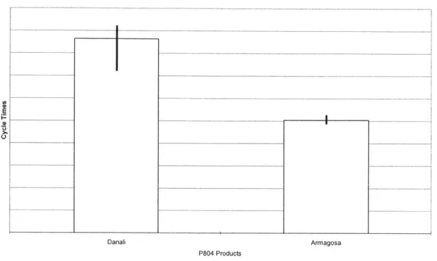
Figure 5.3.3: Variability in Sort 1 Process Time
E8 L) H-
A-rhl
+
±
-k
t
Trumbull 64 Trumbull 32 Trumbull 128 Trumbull 128 Trumbull 256 Sawtooth 84 Whiteciff 64 Danali (discrete) (wafer sales)
---P83Products---P804
0 Median -1st Quartile -3rd Quartile
17
Armagosa
Products---r-6
_lk-Figure 5.3.4: Variability in Sort 2A Process Times
______________ I _______
Danali Armagosa
P804 Products 0 Median 1st Quartile 3rd Quartile
Figure 5.3.5: Variability in Sort 2 Process Times E
2
(.
Trumbull 64 Trumbull 32 Trumbull 128 Trumbull 128 Trumbull 256 Sawtooth 64 Whitecliff 64 Danali (discrete) (wafer sales)
0 Median -1st Quartile 3rd Quartile
Armagosa
Products---I
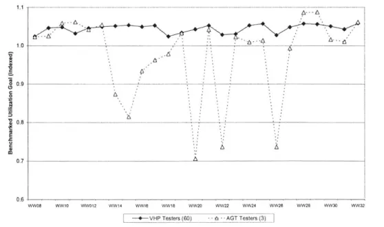
5.4 Tester Utilizations
Sort 23's utilization measure is defined by the amount of time the floor's sorting tester equipment is processing a lot (excluding setup times) divided by the total time the equipment is qualified5 to run the product, or arithmetically:
Utilization = Time Sorting Wafers
Total Time
For each of Sort's tester models (VHP and AGT), the average weekly utilization metric is calculated as:
Numberoftesters #Wafersprocessed
Z
I Time Sorting each WaferWeekly Utilization =
Number of Testers x 168 hours / week
Examining weekly utilization levels (indexed against internal benchmarks, where 1.0 equals target performance) shows consistently high metrics for its fleet of 60 VHP testers but sporadic dips for its three AGT testers (Figure 5.4.1). Clearly, this metric is sensitive to the total number of testers within a model category. For example, in WW26 one of the
AGT testers failed a maintenance diagnostic and experienced considerable down time
from delayed troubleshooting and re-qualification. This single incident caused the AGT utilization to plummet to around 0.75, yet an equivalent downtime on a VHP model tester would only register as a 0.02 drop in that model's weekly utilization (indexed).
Figure 5.4.1 Weekly Utilizations for VHP and AGT Tester Models
.. ... 1.0 0.9 (0 0.8 0.7 0.6
WWOB WWIO WWO12 WW14 ww1e WW18 WW20 WW22 WW24 WW26 WW28 WW30 WW32
---+- VHP Testers (60) - s - -AGT Testers (3)
5 Qualification is an engineering process that certifies individual testers as capable of performing particular processes on particular products. Only equipment which has been qualified may be used to produce product
One of the ways Sort maximizes its utilization metric is by minimizing the lost production time from tester changeover activity. For example, assume a sort tester is setup to run product A with product B already waiting to be tested. If a product A arrives and there is no imminent need for more of product B, the new product A will be loaded onto the equipment ahead of the waiting product B to save a setup changeover from occurring. Similarly, a sort tester processing Sort 1 will continue to operate on Sort 1 until a pressing need requires a change to Sort 2A or Sort 2.
As mentioned before, changeovers can vary from 5 to 45 minutes depending on the range and direction of the operating temperature change. With only a handful of changeovers occurring each shift, the lost tester time typically amounts to between 0.1
% and 0.4 % of the total tester
availability (see Figure 5.4.2 for complete breakdown of tester availability).
Figure 5.4.2: Breakdown of Logbook Data by Tester Status
RUNNING PRODUCT 94.35% DOWN 2.80% IN REPAIR 1.38% MAINTENANCE 0.45% WAITING PRODUCT 0.31% ENGINEERING 0.26% CHANGEOVER 0.21% WAITING PART 0.13% WAITING TECHNICIAN 0.06% MAINTENANCE OVERDUE 0.04%
Total Tester Time 100%
(Data taken from all VHP Testers for 1' 14 weeks of 2004). 5.5 Rework Rates
Rework at Sort 23 is defined by the redundant processing time spent re-sorting a wafer. Figure 5.5 shows the percentage of rework time over total processing time for a period of nearly 5 months. Intel plans for 0.3% rework rates in each of their Sorting operations, which approximately matches the mean values of the observed data.
Figure 5.5 Sort Rework Rates
1.4 1.2 I0 0.8 0.6 0.4 0.2 0 4
WWO6 WW07 WWO8 WWO9 WW10 WW11 WW12 WW13 WW14 WW1 WW16 WW17 WW18 WW19 WW20 WW21 WW22 WW23 WW24
I Sort 1 -A- Sort 2A --O- Sort 2
5.6 Fab 23 Planning and Product Delivery to Sort 23
Each week, Fab 23 starts manufacturing a certain number of wafers per product with a planned lead time of 8 weeks before delivery to Sort. Sort then has a two-week lead time in which to process these wafers and deliver the scheduled die quantities to ADI. Hence, the fab wafer starts are always based on what ADI will need 10 weeks in the future; die-schedules oftentimes change during this lag period. Indeed, die-schedules may change even before a few days of being due. So as the last set of operations before ADI delivery (and
LIPAS scoring), Sort has a de-facto responsibility to monitor and meet these changing die
schedules on a weekly basis.
Figures 5.6.1 and 5.6.2 show the delivery of Fab 23's wafers into Sort 23 during each shift as well as aggregated over a weekly horizon for a period of 17 weeks. Wafer arrivals appear to be highly-variable from shift-to-shift yet roughly consistent on a weekly tally. Notably, fab operations emphasize the execution of wafer delivery, or 'fab outs', on a weekly basis.
Figure 5.6.1 Fab 23 Delivery Rates to Sort 23
(I, 0 (U 0 0 I-0 0 0 ~0-(U 0 2/1 2/8 2/15 2/22 2/29 3/7 3/14 3/21 3/28 4/4 4/11 4/18 4/25 5/2 5/9 5/16 5/23 5/30 --- ---- --- --- --- --- --- --- --- ---
---
---
---
---
---
---
---
---
---
---
---
---
--
---
--- --- - -- -- --- --- --- - - - - -- - - - 1-
1 4
... HHHHH I H"H!"! ""HHHHHHHHHHHHH !"H111H 101HHHHH11 HFigure 5.6.2 Fab 23 Delivery Rates to Sort 23 x 0 0 U (U 0 V 0 0 0 0 (U 2/1 2/8 2/15 2/22 2/29 3/7 3/14 3/21 3/28 4/4 4/11 4/18 4/25 5/2 5/9 5/16 5/23 5/30
In order to satisfy its weekly die-out targets, Sort 23 must allocate their tester capacity by product type and sorting operation. Figure 5.6.3 shows how the delivery of wafers from Fab 23 corresponds to the product-specific loadings necessary for Sort 23 to meet their schedules within their two week lead time. As a customer, Sort sees large swings in the delivery of products from their fab supplier - a dynamic one technician describes as 'feast or famine'.
Figure 5.6.3 Fab Delivery Performance by Product*
900% 750% (J600% . 450% x 300% 150% > A--A" 00% '150% d -300% VVW06 WW07 WWOB WW09 WW10 WW11 WW12 WW13 WW14 WW15 WW16 WW17 WW1l WW19 WW20 WW21 WW22
---- Trumbull 128 -0--- Trumbull 32 - -* - -Trumbull 256 X Trumbull 64 -0-- Sawtooth 64
While both Fab and Sort Operations Managers reference common information reports detailing daily product delivery status from the fab, the communication pathways between the groups are numerous (emails, phone calls, and meetings), complex
(involving dozens of Technicians, several Operating Managers, Planning personnel, and Industrial Engineering liaisons), and crippled by delays; at the point in time when a Sort Technician communicates a need for more Trumbull 32, the Fab managers might easily require 3 to 7 weeks to adjust the delivery rate for this product. This gap in customer-supplier connection leads not only to variability in product inventory levels on the Sort floor but also frustration on the part of Sort personnel to maintain predictable flow to fulfill die schedules.
For the time interval examined, there appears to be more product volume delivered weekly from the fab than is actually needed by Sort's downstream customer, ADI. As an extreme example, the fab delivered approximately ten times the amount of Trumbull 64 in WW1 5 than was necessary to fulfill schedules (only to be balanced by a deficit of 2.5x the next week)! As we will see next, these excessive inflows may cause surges in Sort inventory levels in the near term yet support a steady practice of overproducing beyond scheduled amounts over the longer term.
Since the size of ADI inventories remains manageable at Intel despite this overproduction, one might argue that the final die schedules are systematically
underestimating the real demand of the downstream Assembly operations on ADI. Given the time interval and scope of this thesis research, however, this conclusion is difficult to confirm.
5.7 Production Scheduling Dynamics
Twice a week, each Sort Operations Manager and daytime Area Coordinator meets with the department's Industrial Engineer and a representative from the Fab 23's planning group to discuss anticipated production volumes and product mix over a 2-7 week horizon. Schedule changes from ad-hoc customer requests, changes in fab yields, run times, and equipment availability are all coordinated across these groups during these meetings. Information on the latest schedule is then communicated to the floor by both the OM and AC through email, shift-to-shift pass-down meetings, and informal
discussions.
As an example of these changes, Figure 5.7.1 shows the production schedules for the Trumbull product categories over a period of 18 weeks. The planned product volumes (in wafers, indexed) are broken down into three sequential snapshots in time:
1.) The schedules as they appear two weeks before LIPAS is due
2.) The same schedules once 'fixed' a week before LIPAS is due, and finally
Figure 5.7.1 Schedule Changes and Final Production Volumes Trumbull 128 Discrete 0.9 0.8 0.7 F 0.6 4) 0.5 0.4 0.3 0.2 0.1 0 0.7 0.6 0.5 x 0.4 0.3 0.2 0.1 0 WWo8 WWc9 WW10 WW11 WW12 WW13 WW14 WW15 WW1e WW17 WW18 WW19 WW20 WW21 WW22 WW23 WW24 WW25 WW26 WW27
-0-(Sort Output -X- Schedule @ 1 week to LIPAS A Schedule @ 2 weeks to LPAS
/-
-A
WWO8 WWO9 WW10 WW11 WW12 WW13 WW14 WW15 WW16 WW17 WW18 WW19 WW20 WW21 WW22 WW23 WW24 WW25 WW26 WW27
-0- Sort Output -R- Schedule @ 1 week to LIPAS - Schedule @ 2 weeks to LIPAS
Trumbull 32
-A--
Trumbull 256 0 .6 - _- ~ ~ -0.5 0.4 0.3 0.2 0.1 0 WW08 WW09 WWIO WW11 WW12 WW13 WW14 WW15 WW16 WW17 WW18 WW19 WW20 WW21 WW22 WW23 WW24 WW25 WW26 WW27
-- Sort Output -*-- Schedule @ 1 week to LIPAS -A- Schedule @ 2 weeks to LIPAS
Trumbull 64 1.2 0.8 0.6 0.4 0.2 0 WW08 WWO9 WW10 WW11 WW12 WW13 WW14 WW15 WW16 WW17 WW18 WW19 WW20 WW21 WW22 WW23 WW24 WW25 WW26 WW27
Two interesting trends emerge from this viewpoint. First, as delivery dates become more immediate (i.e. the horizon closes from 2 weeks to 1 week), the scheduled volumes seem to drop across many of the product categories and weeks. However, comparing these final 'fixed' schedules to the volumes that Sort actually delivers to ADI shows a systematic trend in Sort consistently delivering wafers beyond the final schedule amounts.
One key reason for this dynamic stems from a policy of accruing all overproduction as credit in future week's schedules. For example, if Sort ships 100 die of Trumbull 128 beyond their weekly target, then planning will lower their production schedule by 100 units the subsequent week. On the one hand, the practice of shipping ahead of schedule allows Sort to smooth large peaks in scheduled demand through early accruals, mitigating large fluxes in tester changeovers. On the other hand, overproduction is a clear signal that schedules are lax relative to the output performance of the floor. Notably, Sort only missed a final die schedule three times over the course of 18 weeks studied; if Sort were held to the die schedules set two-weeks away from the delivery due dates, they would have missed their schedules 56 times!
Since overproduction is a normal practice, a tier catalogue is used to coordinate the product priorities from delivery to ADI across all of Intel's Fab/Sort operations. Figure 5.7.2 shows how tier assignments optimize output levels across product categories subject to scheduling volumes.
Figure 5.7.2 Tier Priorities for Product Delivery to ADI
Priority Description
Tier I Maximize output. Subordinate other schedules to overship if possible.
Tier 2 Hit schedules. Once schedule is hit, do not subordinate Tier 3 schedules to overship schedules. Tier 3 Maximize performance to schedule. But not at expense of Tier 1 & 2 expectations.
Tier 4 Prioritize behind Tier 1-3. Only run if you have idle testers or you are on track to make all Tier 3 schedules.
Hence, an over-shipment of Tier 3 product while missing a Tier 2 schedule would constitute a misallocation of tester capacity for Sort 23. It is difficult to measure how strictly Sort performs to these guidelines given the complex variables that determine each product's overproduction; the tier catalog prioritization must be considered alongside any future peaks in schedule volume (spurring early accruals and smoother production
volumes across multiple weeks) as well as limits from the delivery of product from the fab (constraining the amount of accrual possible).
As a rough gauge of performance, Figure 5.7.3 shows the tier priorities and Sort's over-shipments during weeks 15 and 16 across all products. From this limited perspective, Sort
23 appears to be lax in adhering to the tier priorities rules; the excess delivery of
Armagosa 32 above schedules is especially suspicious when ranked against the higher-priority, lower-volume delivery of Trumbull 32.
Figure 5.7.3 Overproduction across Tier Priorities in Work Week 15 and 16
Work Week 15
3
1~
N:-2
32M Trumbull 64M Sawloth 64M Trumbull 128M D
F l
-anali 128M Trumbull D 128M Trumbull 256M Trumbull 32M Armagosa 64M Whitecliff
ws Tier Priority -+- Ship Aheads
Work Week 16 7flfu% 600% 500% 400% 300% .. ~ 200%o 100% 0/%
128M Danali 32M Trumbull 64M Trumbull 128M Trumbull D 128M Trumbull WS 256M Trumbull 32M Armagosa 64M Sawtooth
i Per Pnorty -+-Ship Aheads E z Rt 120% 100% 80% 60% o C 40% 0. 20% 0% z 3 2 U 0 (L
5.8 Capacity Management Systems
The Sort Area Coordinators have developed spreadsheets that estimate the minimum number of testers that must be setup on each product and each sort operation to fulfill the current mix of die schedules. Given a series of sorting operations i and products
j,
the tester estimates for any given week can be calculated as follows:Let
Qj
= the remaining quantity of scheduled die for productj
Rij = process time required to sort each wafer of product
j
at sorting operation iDj = the fixed die-per-wafer ratio
Yj = the historical die yield for product
j
T = the amount of time left before the delivery due date
The whole number tester estimate Sij for each sorting operation i and product
j
isSU = ROUND U DY
where the total sum of available testers must not be exceeded, or
Sorting To talI#of
Operations Pr oducts
I I SU (total sort testers)
i=1 j=1
Notably, fractional tester quantities are always rounded up to promote over (versus under) production. The capacity estimates also assume 100% tester utilizations, 0% resorting rates, and deterministic run rates and die yields. Given these uncertainties, the model is iteratively updated with quantities
Qj
throughout the week as production due dates advance and time horizon T decreases.For example, let's assume product A has 200 die per wafer, product B has 750 die per wafer, and that each product has an historical yield of 85% and 95%, respectively.
Furthermore, let's assume we know that the run times for the Sort 1 and Sort 2 operations are 1 and 2 hours per wafer for product A and 1.5 and 3.5 hours per wafer for product B. Finally, at a time of 168 hours before schedules are due we have 625,000 die of product
A and 435000 die of product B yet to deliver:
Product Die per Historical Run time per Run time per Remaining
() Wafer Die Yield wafer for Sort 1 wafer for Sort 2 Die Due (Q)
(Di) (Yi) (Ri=1) (Ri=2)
A 200 85% 0.75 hours 1 hour 625,000
B 750 95% 2 hours 3.5 hours 435,000