HAL Id: tel-00926053
https://tel.archives-ouvertes.fr/tel-00926053
Submitted on 9 Jan 2014
HAL is a multi-disciplinary open access
archive for the deposit and dissemination of sci-entific research documents, whether they are pub-lished or not. The documents may come from teaching and research institutions in France or abroad, or from public or private research centers.
L’archive ouverte pluridisciplinaire HAL, est destinée au dépôt et à la diffusion de documents scientifiques de niveau recherche, publiés ou non, émanant des établissements d’enseignement et de recherche français ou étrangers, des laboratoires publics ou privés.
Optical Properties of Nd-Doped Si-based thin films :
towards an optical amplifier
Chuan-Hui Liang
To cite this version:
Chuan-Hui Liang. Optical Properties of Nd-Doped Si-based thin films : towards an optical amplifier. Materials Science [cond-mat.mtrl-sci]. Université de Caen, 2013. English. �tel-00926053�
Université de Caen Basse-Normandie
Ecole doctorale SIMEM
Thèse de doctorat
présentée et soutenue le : 28/11/2013 par
Chuan-hui LIANG
pour obtenir le
Doctorat de l’Université de Caen Basse-Normandie
Spécialité : Milieux denses, matériaux et composants
Propriétés optiques des films minces à base de Si dopé Nd :
Vers un amplificateur optique
Directeur de thèse : Fabrice Gourbilleau
Jury
M. Bruno Masenelli Professeur des Universités, INSA Lyon-INL (Villeurbanne) (rapporteur).
M. Hervé Rinnert Professeur des Universités,Université de Lorraine- Institut Jean Lamour (Nancy) (rapporteur)
Mme. Marie-Paule Besland Directrice de Recherche CNRS,IMN (Nantes) (Examinatrice) M. Julien Cardin Ingénieur de Recherche,CIMAP (Caen) (co-directeur de thèse) M. Fabrice Gourbilleau Directeur de Recherche CNRS, CIMAP (Caen) (directeur de
thèse)
i
Contents
List of Figures ... iii
List of Tables ... viii
List of Abbreviations ... ix
General Introduction
... 1Bibliography ... 5
Chapter 1: Rare earth Si-based layers
... 71.1 Si Nanostructure ... 7
1.1.1 Comparison with Si bulk ... 7
1.1.2 Fabrication ... 8 1.1.3 Optical properties ... 8 1.1.4 Devices ... 13 1.2 Er and Si nanostructure ... 13 1.2.1 Introduction ... 13 1.2.2 Fabrication ... 14 1.2.3 Optical properties ... 15 1.2.4 Devices ... 17 1.3 Nd and Si nanostructure ... 18 1.3.1 Introduction ... 18 1.3.2 Nd-doped Matrices ... 20 1.3.3 Devices ... 22 1.4 Conclusion: ... 22 Bibliography ... 24
Chapter 2 Experimental techniques and analytical methods
... 292.1 Thin film fabrication ... 29
2.1.1 RF Magnetron Sputtering ... 29
2.1.2 Annealing ... 33
2.2 Sample characterization ... 34
2.2.1 Fourier transform infrared spectroscopy ... 34
2.2.2 Spectroscopic ellipsometry ... 38
2.2.3 Raman spectroscopy ... 45
2.2.4 Photoluminescence spectroscopy ... 47
Bibliography ... 52
Chapter 3: A study on Nd doped Si-rich silicon oxide films
... 533.1 Introduction ... 53
3.2 Effect of Si excess incorporated ... 54
3.2.1 Fourier transform infrared spectroscopy ... 54
3.2.2 Ellipsometry ... 56
3.2.3 Estimation of Si excess ... 58
3.2.4 Optimal Si content ... 60
3.3 Effect of Nd content incorporated ... 66
3.3.1 Estimation of Nd content ... 66
3.3.2 Photoluminescence properties ... 69
3.4 Effect of annealing conditions ... 70
3.4.1 Annealing temperature for RTA approach ... 70
3.4.2 Annealing temperature for CA approach ... 74
3.4.3 Annealing duration ... 77
3.4.4 Forming gas annealing ... 80
3.5 Energy transfer mechanism ... 82
3.5.1 PL properties for SiOx films ... 82
3.5.2 Compared the PL properties of SiOx to Nd-SiOx film ... 85
3.5.3 Interactions between sensitizers and Nd3+ ions ... 91
ii
Bibliography ... 95
Chapter 4: A study on Nd doped Si-rich silicon nitride films
... 974.1 Introduction ... 97
4.2 Effect of Si excess incorporated ... 97
4.2.1 Fourier transform infrared spectroscopy ... 97
4.2.2 Ellipsometry ... 99
4.2.3 Estimation of Si excess ... 100
4.2.4 Optimal Si content ... 102
4.3 Effect of Nd content incorporated ... 104
4.3.1 Estimation of Nd content ... 104
4.3.2 Optimal Nd content ... 106
4.4 Effect of annealing conditions ... 107
4.4.1 Annealing temperature for RTA approach ... 107
4.4.2 Annealing temperature for CA approach ... 111
4.4.3 Annealing duration ... 114
4.4.4 Forming gas annealing ... 115
4.5 Energy transfer mechanism ... 117
4.6 Conclusion ... 119
Bibliography ... 120
Chapter 5: Devices based on Nd-SRSO and Nd-SRSN materials
... 1215.1 Introduction ... 121
5.2 Device fabrication ... 122
5.3 Optical properties ... 125
5.3.1 Optical losses ... 125
5.3.2 Guided photoluminescence ... 126
5.3.3 Pump and probe measurements ... 133
5.4 Conclusion ... 135
Bibliography ... 136
iii
List of Figures
Chapter 1
1.1 (a)-(d) correspond to SRSO samples, (a) PL spectra of 5.6 at.% Si excess samples annealed at indicative temperatures, (b) PL spectra of different Si excess samples annealed at 1200°C, (c) the full width at half maximum of PL peak vs Si excess, and (d) PL intensity vs annealing temperature, while (e)
comparison of PL spectra of SRSO (closed symbols) and SRSN (open symbols) films ... 9
1.2 (a) Electronic states in crystalline Si-nps vs their diameter, and (b) average HOMO-LUMO band gap of amorphous Si-nps (a-Si-nps) compared to that of crystalline Si-nps (c-Si-nps) ... 11
1.3 Non-single exponential PL decays measured (a) at room temperature for samples fabricated by reactive magnetron sputtering; and (b) at the indicative temperatures for sample containing 18 at.% Si excess ... 12
1.4 Illustration of energy transfer from Si-nps to Er3+ ions ... 14
1.5 (a) PL spectra of Si nanocrystal-doped SiO2 containing different Er content in the range of 0-1.8 at.%, and (b) decay curves of Si nanocrystal dependence on Er content ... 16
1.6 Waveguide amplifier based on co-doped of Si-nps and Er in Si-based film adopting vertical pump sources supplied by low-cost LEDs ... 18
1.7 Illustration of energy transfer from Si-nps to Nd3+ ions ... 19
1.8 Nd3+ concentration dependence of lifetimesboth for 0. 92-µm-Nd3+ PL fitted by two exponential laws. The inset shows its typical decay curve with fitting line ... 21
Chapter 2 2.1 Diagram of the AJA Sputtering chamber with cathodes, glowing plasma, and the diagrammatic representation of various processes during sputtering ... 29
2.2 Schematic diagram of the annealing process ... 33
2.3 Different vibration types for chemical bonds ... 35
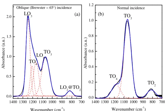
2.4 FTIR spectra of as-deposited SiO2 film which are decomposed into six Gaussians at Brewster incidence (a) and three Gaussians at normal incidence (b). Black line is experimental curve, and blue line is the result of superimposition of the Gaussian curves ... 36
2.5 FTIR spectra of as-deposited silicon nitride film measured (a) with an incidence angle of 65º and (b) with a normal incidence. Black line is experiment curve, and red line is the result of superimposition of the Gaussian curves ... 37
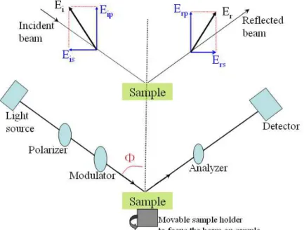
2.6 Schematic diagram of the principle and experimental setup for an ellipsometer ... 39
2.7 (a) Schematic illustration of the film structure and (b) the recorded spectra (square) with their fitting curves (line) ... 41
2.8 Optical properties versus incident photon energy ... 42
2.9 Schematic representation of Raman spectrometer ... 45
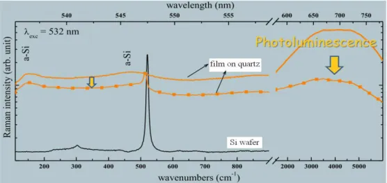
2.10 Raman spectra of Si wafer (black curve), 750°C-annealed (orange curve) and 1100°C-annealed (orange square) SRSN layers deposited on quartz ... 46
2.11 Illustration of excitation and de-excitation processes ... 47
2.12 Schematic diagram of the continuous wave laser PL setup ... 49
iv Chapter 3
3.1 FTIR spectra of as-deposited Nd-SRSO layers recorded at (a) Brewster incidence and (b) normal incidence (all absorbance spectra are offset in perpendicular axis for clarity) – Effect of hydrogen rate rH from 40% to 80% on the film structure ... 54 3.2 FTIR spectra of as-deposited samples recorded at (a) Brewster incidence and (b) normal incidence (all
absorbance spectra are offset in perpendicular axis for clarity) – Effect of power density of Si cathode
ranging from 1.04 to 1.78 W.cm-2 on the film structure ... 55
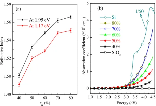
3.3 Evolutions of (a) refractive index with rH and (b) absorption coefficient with energy for as-deposited
layers for different rH ranging from 40 to 80% ... 56
3.4 Evolutions of (a) refractive index with RFPSi and (b) absorption coefficient with energy for as-grown
films for different RFPSi ranging from 1.04 to 1.78 W.cm-2 ... 57
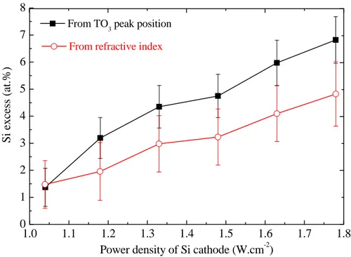
3.5 Si excess evolution with RFPSi with experimental error bars for classical co-sputtered samples analyzed by FTIR spectra and ellipsometry experiments ... 60
3.6 PL spectra for different hydrogen rate rH (from 40% to 80%): (a) as-grown samples and (b)
750°C-1min-annealed samples excited at non-resonant wavelength for the Nd3+ ions (488 nm) ... 61
3.7 PL spectra of (a) as-deposited samples deposited at 500°C and (b) 750°C-1min-annealed samples used
RFPSi ranging from 1.04 to 1.78 W.cm-2. The excitation wavelength is 488 nm which is non-resonant
for the Nd3+ ions ... 62
3.8 (a) Nd3+ PL decay curves of 750ºC-1min-annealed films deposited with different RFPSi, (b) a typical
decay curve of Nd3+ PL with its fitting, (c) Evolution of the Nd3+ lifetimes with RFPSi as well as
refractive index. The excitation wavelength is 488 nm which is non-resonant for the Nd3+ ions ... 63
3.9 (a) Visible PL spectra for 750ºC-1min-annealed samples deposited with various Si target power density. The excitation source is a 450 W Monochromatic xenon lamp at 280 nm. (b) Absorption spectrum for
Nd3+ doped SiO2 film ... 64
3.10 FTIR spectra recorded at Brewster incidence for samples deposited with the indicative RFPNd2O3,
while the inset corresponds to normal incidence ... 66 3.11 Evolutions of (a) refractive index and (b) absorption coefficient with the energy for samples deposited
with the indicative RFPNd2O3 ... 67
3.12 A typical RBS spectrum of film deposited with RFPNd2O3 = 0.3 W.cm-2 and RFPSi= 1.48 W.cm-2. The
inset shows an enlargement in the 350-500 channels region ... 67
3.13 PL spectra of (a) as-deposited and (b) 750ºC-1hour-annealed samples deposited with RFPSi= 1.48
W.cm-2 and for different RFPNd2O3 in 0.3-0.9 W.cm-2 range. The excitation wavelength is 488 nm
which is non-resonant for the Nd3+ ions ... 69
3.14 FTIR spectra recorded at Brewster angle of 65º for as-deposited (AD) and 1min-annealed Nd-SiOx
films at indicated TA temperature. The spectra were normalized to the intensity of one at the top of TO3
band ... 70
3.15 FTIR spectra of typical Nd-SiOx (solid) and Nd-SiO2 (hollow) films, collected at normal incidence for
as-deposited (AD) and indicative TA-1min-annealed samples. Inset shows the y values in SiOy phase
versus TA ... 71
3.16 Raman spectra of the Nd-SiOx films deposited on quartz substrate and annealed at indicated TA for 1
min ... 72
v
by a 488 nm excitation wavelength non-resonant for the Nd3+ ions ... 73
3.18 FTIR spectra recorded at Brewster angle of 65º for as-deposited (AD) and 1hour-annealed Nd-SiOx
films. The films were annealed at indicated TA ... 74
3.19 Raman spectra of the Nd-SiOx films deposited on quartz substrate before and after 1hour-annealing at
1100ºC. Both spectra of quartz substrate and bulk crystalline Si wafer peak are also shown ... 75 3.20 Evolution of PL spectra of samples before and after annealing at the indicative temperature for 1 hour
duration. The excitation wavelength is 488 nm which is non-resonant for the Nd3+ ions ... 76
3.21 (a) bright field and (b) dark field images for 1min-1100ºC-annealed layer, (c) bright field and (d) dark field for images for 1hour-1100ºC-annealed layer. The layer thickness is about 370 nm. The present Si-nps are highlighted by a circle ... 77 3.22 PL spectra of samples annealed for the indicative duration at 750ºC (left) and 1100ºC (right). The
excitation wavelength is 488 nm which is non-resonant for the Nd3+ ions ... 78
3.23 Nd3+ PL decay curves of Nd-SiOx films (a) annealed at 750ºC and (b) at 1100ºC for the indicative
duration. (c) A typical decay curve of Nd3+ PL with its fitting, (d) Evolution of the Nd3+ lifetimes with
annealing time. The excitation wavelength is 488 nm which is non-resonant for the Nd3+ ions ... 79
3.24 PL spectra for samples annealed at 750ºC during (a) 1min. and (b) 30 min. under N2 gas (solid) and
FG ambient (hollow), respectively. The excitation wavelength is 488 nm which is non-resonant for the
Nd3+ ions ... 80
3.25 PL spectra of samples annealed at the indicative TA and tA. The black curves with solid symbol
correspond to annealing under N2 gas, while the red ones with hollow symbol concern the two steps
annealing process. The FG in this figure represents a 500ºC-5hour-annealing under forming gas
ambient. The excitation wavelength is 488 nm which is non-resonant for the Nd3+ ions ... 81
3.26 The PL spectra of SiOx films annealed at the indicative temperature during 1 minute. The left graph (a)
corresponds to TA lower than 1000°C while the right one (b) to high TA higher than 1000°C. AD is the
abbreviation of as-deposited. The excitation wavelength is 488 nm ... 82
3.27 Integrated peak intensity (left) and peak maximum position (right) of SiOx films versus TA ... 83
3.28 EL and EH integrated peak intensity versus tA for SiOx films annealed at 750°C (left scale) and 1100°C
(right scale), respectively. The excitation wavelength is 488 nm ... 84
3.29 PL spectra of Nd-SiOx and SiOx films annealed at 750°C during (a) 1 minute and (b) 1 hour. The
excitation wavelength is 488 nm which is non-resonant for the Nd3+ ions ... 85
3.30 Integrated peak intensities of Nd-SiOx and SiOx films annealed at 750°C versus tA. The excitation
wavelength is 488 nm which is non-resonant for the Nd3+ ions ... 86
3.31 PL spectra of both Nd-SiOx and SiOx films annealed for 1 minute at 1100°C. The excitation
wavelength is 488 nm which is non-resonant for the Nd3+ ions ... 87
3.32 Evolution of PL lifetimes measured on peak EL and EH versus TA for 1min-annealed SiOx and Nd-SiOx
films excited at 488 nm and detected at the maximum point of each peak. The inset shows the PL
decay curves for SiOx films annealed at 750 and 1100ºC ... 88
3.33 Evolution of Nd3+ PL lifetime at 920 nm versus TA. The inset (a) is a representative decay rate of
750ºC Nd-SiOx PL, fitted by a two-exponential decay model, while the inset (b) is the component of
Nd3+ fast or slow lifetime ... 90
3.34 Schematic illustrations of the Nd3+ ions excitation. (i) Energy diagrams of atomic scale sensitizers
vi
(b) absorption spectrum of Nd3+ ions doped in SiO2 film, and (iii) energy diagram of Si-nps within the
films annealed at TA > 1000°C. ET is the abbreviation of energy transfer ... 91
Chapter 4
4.1 FTIR spectra recorded with (a) an incidence angle of 65º and (b) a normal incidence for as-deposited
Nd-SRSN layers produced by the indicated N2/(N2+Ar) nitrogen rates (rN). ... 97
4.2 For as-deposited layers, (a) refractive index evolution as a function of the nitrogen rate rN for two
energies, 1.17 and 1.95 eV; (b) absorption coefficient versus energy from 1.0 to 4.5 eV for different rN
investigated and pure Si3N4 and Si layers ... 99
4.3 Si excess evolution versus rN with experimental error bars for classical co-sputtered samples. The Si
excess values have been deduced from FTIR and ellipsometric measurements ... 102
4.4 PL spectra for different nitrogen rates rN from 7.0% to 13.3% in (a) as-grown samples and (b)
750ºC-1min-annealed samples. The excitation wavelength (488 nm) is non-resonant with the energy
levels of the Nd3+ ions ... 103
4.5 FTIR spectra recorded with (a) an incidence angle of 65º and (b) a normal incidence for as-deposited
samples fabricated with the indicated RFPNd2O3. The curves have been normalized with respect to the
TO band intensity. ... 104 4.6 Evolutions of (a) refractive index and (b) absorption coefficient for as-deposited samples with the
indicated RFPNd2O3 ... 105
4.7 PL spectra for (a) as-deposited and (b) 750ºC-1min-annealed samples fabricated with the indicated RFPNd2O3. The excitation wavelength (488 nm) is non-resonant with the energy levels of the Nd3+ ions ... 106 4.8 FTIR spectra recorded with (a) an incidence angle of 65º and (b) a normal incidence for the Nd-SRSN
layers as-deposited (AD) and 1min-annealed at the indicated temperatures (TA). The curves have been
normalized with respect to the TO band intensity ... 107
4.9 Raman spectra of the samples deposited with the indicative nitrogen rate rN and 1min-annealed at the
indicated TA. The samples were prepared with RFPNd2O3 and RFPSi of 0.45 and 4.5 W.cm-2,
respectively ... 108
4.10 PL spectra for as-deposited and 1min-annealed samples (at indicated TA). The sample was prepared
with rN, RFPNd2O3 and RFPSi of 10.5%, 0.45 and 4.5 W.cm-2, respectively. The inset shows the
integrated PL intensity for 920 nm peak versus TA. The excitation wavelength (488 nm) is
non-resonant with the energy levels of the Nd3+ ions ... 109
4.11 FTIR spectra recorded with (a) an incidence angle of 65º and (b) a normal incidence for the Nd-SRSN layers as-deposited (AD) and 1hour-annealed at the indicated temperatures. The sample was prepared
with rN, RFPNd2O3 and RFPSi of 10.5%, 0.45 and 4.5 W.cm-2, respectively. The curves have been
normalized with respect to the TO band intensity ... 111 4.12 Raman spectra of the as-deposited and 1hour-annealed Nd-SRSN films at 900 and 1100°C. The layers
have been deposited on fused silica with RFPNd2O3= 0.45 W.cm-2, RFPSi=4.5 W.cm-2, and indicated rN ... 112
4.13 PL spectra for samples under 1hour-annealing at the indicated temperatures. The sample was deposited
with RFPNd2O3=0.45 W.cm-2, RFPSi=4.5 W.cm-2, and rN=10.5%. The excitation wavelength (488 nm) is
non-resonant with the energy levels of the Nd3+ ions ... 113
4.14 Evolution of PL spectra versus annealing duration from 1 to 60 min for samples annealed at 750ºC (a)
and 1100ºC (b). The sample was deposited with RFPNd2O3=0.45 W.cm-2, RFPSi=4.5 W.cm-2, and
vii
4.15 PL spectra of samples annealed at 750ºC for (a) 1 min and (b) 30 min duration under N2 gas (black
solid) and FG ambient (red hollow), respectively. The 488 nm excitation wavelength is non-resonant
with the energy levels of the Nd3+ ions ... 115
4.16 PL spectra of samples annealed at the indicative TA for 1 min duration. The black curves with solid
symbol correspond to annealing under N2 gas, while the red curves with hollow symbol concern two
steps annealing. The FG in this figure represents a 500ºC-5hour-annealing under forming gas ambient.
The 488 nm excitation wavelength is non-resonant with the energy levels of the Nd3+ ions ... 116
4.17 PLE spectra detected at 920 nm for three samples (rN=9.5%, 10.5%, and 11.8%) annealed at 750ºC for
1 min duration. The curves correspond to different perpendicular scales classified by their color ... 117 4.18 Estimation of optical band gap for three samples (rN=9.5%, 10.5%, and 11.8%) annealed at 750ºC for
1 min duration ... 118 Chapter 5
5.1 Schematic representations of (a) planar waveguide and (b) rib loaded waveguide ... 123 5.2 Dispersion of modes as a function of the thickness of (a) Nd-SRSO and (b) Nd-SRSN guiding layers for
TE and TM polarization at 1064 nm ... 124
5.3 Evolution of factor of merit (FOM) as a function of the SiO2 rib layer thickness t3 shown in the inset ... 124
5.4 Schematic diagrams describing the different steps required for fabricating the rib waveguide ... 125 5.5 (a) Schematic representation of the top surface pumping at 488 nm and near-field of guided PL at the
output of planar optical waveguide, (b) energy levels for Nd3+ ion radiative transitions, (c) comparison
of guide PL spectra for Nd-SRSO and Nd-SRSN planar waveguides obtained by top-pumping ... 127 5.6 (a) Evolution of guided PL spectra obtained by top surface pumping, for different values of the pump
power on Nd-SRSO planar waveguides. In the inset: integrated PL for the two emissions
corresponding to 4F3/2-4I9/2 (850-1000 nm) and 4F3/2-4I11/2 (1000-1200 nm) radiative transitions versus
pump power, (b) Evolution of guided PL spectra obtained by top surface pumping for different values of the pump power on Nd-SRSN planar waveguides. In the inset: integrated PL for the two emissions
corresponding to 4F3/2-4I9/2 (850-1000 nm) and 4F3/2-4I11/2 (1000-1200 nm) radiative transitions versus
pump power ... 128 5.7 (a) Schematic representation of the top surface pumping at 488 nm, (b) Evolution of guided PL spectra
for different distances z which corresponds to the distance between the excitation area and the output of the waveguide for Nd-SRSO planar waveguides. In the inset: integrated PL versus distance z for the
two emissions corresponding to 4F3/2-4I9/2 (850-1000 nm) and 4F3/2-4I11/2 (1000-1200 nm) radiative
transitions, (c) Evolution of guided PL spectra for different distances z, which corresponds to the distance between the excitation area and the output of the waveguide for Nd-SRSN planar waveguides.
In the inset: integrated PL versus distance z for the two emissions corresponding to 4F3/2-4I9/2
(850-1000 nm) and 4F3/2-4I11/2 (1000-1200 nm) radiative transitions ... 130
5.8 Schematic diagram of pump and probe measurements ... 133 5.9 Measured signals for the pump and probe experiments of Nd-SRSO waveguide ... 134
viii
List of Tables
2.1 Parameters of CA and RTA in four steps ... 33 2.2 Estimation of atomic concentration in SRSO materials ... 43 2.3 Estimation of atomic concentration in SRSN materials ... 44 3.1 Si excess estimated using FTIR experiments in left part and refractive index in right part for reactive
(top) and classical (bottom) co-sputtered samples. The uncertainty of WTO3 value is 1 cm-1 while for
n value is 0.002 ... 58 4.1 Si excess is estimated by FTIR in left part and from refractive index n in right part for the
as-deposited samples. The uncertainty of WLO value is 1 cm-1 while n value is 0.002 ... 100
5.1 Optical losses values (dB.cm-1) as a function of the wavelength for undoped and Nd-doped planar
ix
List of Abbreviations
• AD - As-deposited
• ASS - Atomic Scale Sensitizers
• BEMA - Bruggeman Effective Medium Approximation
• CA - Classical Annealing
• CCD -
• c-Si - Crystalline Silicon
• DC - Direct Current
• EDWA - Erbium-doped Waveguide Amplifier
• EMA - Effective Medium Approximation
• FG - Forming Gas
• FTIR - Fourier Transform Infrared Spectroscopy
• FWHM - Full Width at Half Maximum
• LCs - Luminescence Centers
• LEDs - Light Emitting Diodes
• LDOS - Local Density of States
• LO - Longitudinal Optical Mode
• MBE - Molecular Beam Epitaxy
• NBOHCs - Non-Bridging Oxygen Hole Centers
• ODCs - Oxygen-Deficient Centers
• OPO - Optical Parametric Oscillator
• PECVD - Plasma Enhanced Chemical Vapor Deposition
• PL - Photoluminescence
• PLE - Photoluminescence Excitation
• ppls - Plasma Pressure
• QCE - Quantum Confinement Effect
• RBS - Rutherford Backscattering Spectroscopy
• RE - Rare Earth
• RF - Radio Frequency
• RFPSiO2 - RF power density applied onto SiO2 cathode
• RFPSi - RF power density applied onto Si cathode
x
• rH - Hydrogen rate • rN - Nitrogen Rate
• RTA - Rapid Thermal Annealing
• SE - Signal Enhancement
• Si-nps - Silicon nanoparticles
• SiNx - Silicon rich Silicon Nitride • SiOx - Silicon rich Silicon Oxide • SRSN - Silicon rich Silicon Nitride
• SRSO - Silicon rich Silicon Oxide
• TA - Annealing Temperature
• tA - Annealing Time
• Ts - Substrate Temperature
• TEM - Transmission Electron Microscopy
1
General Introduction
(a) State of the art
The last decades of the 20th century witnessed the emergence of Information Era occurring of data exchange across the world. Such phenomenon has significantly promoted the industrial development of information technology. This “digital explosion” is the result of the invention of internet and computer, whose development is closely connected to the microelectronic technology. Since several decades, the microelectronic industry is striving for further reduction in the size of transistor, following the famous Moore’s law. However, these highly miniaturized devices are now facing the so called electronic bottleneck. Because the electronics have significant challenges to meet the increasing requirements on information transmission of high speeds, large capability, and low noise. The decreasing of feature sizes and increasing clock frequencies among inter-chips or extra-chips would beat the physical limitation of electrical signaling[ 1 ]. Moreover, the dissipation of electric power limits the efficiency of complementary metal-oxide semiconductors microelectronics.
To overcome these issues, one viable solution lies in the monolithic integration of photonics with semiconductor microelectronics to ensure effective and fast connection of inter-chips or extra-chips. Integrated optics is capable of signal modulating, wavelength multiplexing, switching and amplification. The photonics could bring new functionalities to electronic components such as a higher bandwidth due to higher frequency provide by the carrier optical wave signal, and immunity to electromagnetic perturbations.
One of the critical issues to achieve complete integrated optic system is the lack of integrated light sources. Si-based light source would be one of the most promising candidates for that purpose. Since the Si-based optoelectronic circuit is compatible with CMOS technology, providing the possibility to achieve a compact Si-based device combining the two “electronic and photonic” functions.
In the last 20 years, the research community has taken great interest in the rare earth (RE) ions and Si nanoparticles (Si-nps) coupled system, which is a promising candidate for the achievement integrated Si-based light source. Since the RE ions are benefited from the higher absorption cross section of Si-nps (about 10-16 cm2[2] with respect to 10-20 cm2 for RE ions in SiO2[3]). In this regard, the most addressed is Er3+ ion due to its attractive application
for optical communication[4] in C band. However, evidence of the achievement of net gain from Si-nps : Er3+ ions in such system has been reported only once[5]. This is mainly due to the three-level nature of the Er3+ ions which lead to a threshold pump power to get population
2
inversion. The possibility of re-absorption of emitted photon by the neighboring Er3+ ions is also a potential drawback of using such ions. Since the wide applications for medicine and communication technologies (O band), the Nd3+ ion has aroused great interest. Contrarily to the Er3+ ion, Nd3+ ion emits in four-level configuration (1.06 µm) and does not have a threshold pump power for inversing population and has a weak probability of re-absorption of the emitted light at 1.06 µm. Consequently, net gain seems to be achievable with Nd3+ ion in an easier manner than with Er3+ ion.
However, there are some limitations to achieve sufficient gain of Nd3+ luminescence. The Si-nps with small size are favorable to effectively sensitize the Nd3+ ions, while a high Si excess incorporated would leads to grow large Si-nps. The rather low solubility of Nd within silica[6] leading to the formation of Nd2O3 cluster at the expense of Nd3+ density is another
limiting factor. Such cluster may favor energy migration and cross relaxation leading to a quench of Nd3+ emission. As a result, Debieu et al.[7] have found that the Nd3+ PL decreases dramatically when Nd content increases from 0.08 to 0.27 at.%. Furthermore, the Nd3+ PL decay time is in the order of µs, and may decrease with increasing Si atom excess. Nevertheless, the improvement of the layers microstructure and of Si-nps and Nd3+ ions densities may result in a larger Nd3+ population inversion and a higher gain.
(b) Major objectives of this thesis
For an achievement of Si-based Nd3+ laser, this thesis focuses on four major issues which are:
Material growth technique: Both classical and reactive co-sputtering approaches are concerned for the layers grown in our laboratory. One main factor governing the material and device properties is the layer composition, which is closely dependant on the deposition conditions. Therefore, the first major objective of this thesis is to find a suitable deposition approach and then to optimize the parameters (such as Si and or Nd2O3 cathode power
density) to fabricate two typical systems Nd-doped Si-rich silicon oxide (Nd-SRSO) and silicon nitride (Nd-SRSN).
Annealing treatments: Annealing is necessary to improve the quality of the host matrix and form the sensitizers. But a too high temperature and/or too long duration are supposed to result in formation of RE ions clusters as well as overgrowth of Si-nps, which are detrimental to the sample emission intensity. Therefore, the second major objective of this work is to optimize annealing conditions (temperature, duration, and gas atmosphere) involving the classical annealing and rapid thermal annealing.
3
Material properties: Photoluminescence (PL) measurements help one to select the optimal sample which provides the most possibility to obtain net gain. Achieving significant Nd3+ PL is a challenge, and understanding the mechanisms of energy transfer from sensitizers becomes the next important challenge. Therefore, the third major objective of this work is to analyze the microstructural properties of the materials, to correlate such microstructure with the PL properties, and to understand the nature of sensitizers towards Nd3+ ions in SRSO and SRSN host matrices.
Device properties: The optimized films were used to fabricate optical waveguides. The possibility of achievement of net gain in such structure would have a large impact towards the realization of a Si-based Nd3+ laser. Therefore, the last major objective is to carry out the investigation of waveguide properties such as losses, guided PL and the signal enhancement measurement.
(c) Sketch of this thesis
There are five chapters in this thesis.
Chapter 1 describes the current research state of Si nanostructure and its coupling with RE ions (Er3+ and Nd3+ ions). This chapter presents the samples fabrication and the optical properties concerning two kinds of host matrices SRSO and SRSN. We focus on the correlations between film composition, microstructure and PL properties.
Chapter 2 shows the principle and the working method of various experimental techniques employed in this thesis for the layer deposition and characterization.
Chapter 3 focuses on the optimization process for Nd-SRSO films. We detail the effects of Si excess and Nd content on structural and optical properties of samples deposited by reactive and classical co-sputtering approaches. The best sample obtained from the latter approach is used to study the influence of annealing conditions. Both classical annealing and rapid thermal annealing are employed with monitoring the temperature, duration, and gas atmosphere. The structural and optical properties of samples are analyzed. With achieving the remarkable Nd3+ PL, the energy transfer mechanism is investigated by comparison to the PL properties of undoped SRSO film.
Chapter 4 is devoted to the study on Nd-SRSN films deposited only by reactive co-sputtering method. The incorporated Si excess is controlled by the nitrogen ratio to the argon gas used in the plasma, while Nd content by the power density applied on Nd2O3
4
film receives classical annealing and rapid thermal annealing with various temperatures and durations. Then the annealed samples are analyzed for structural and optical properties. The PL excitation measurements are performed to study the energy transfer mechanism.
Chapter 5 presents the fabrication of waveguide devices and investigation of the devices optical properties. Optical losses, guided PL, and pump and probe measurements are studied on both kinds of devices made of Nd-SRSO and Nd-SRSN materials. We finish with a summary of this thesis and future perspectives for such Nd-doped Si-based materials.
5
Bibliography
[1] G. T. Reed, A. P. Knights, Silicon Photonics: An Introduction, Spinger-Verlag, Berlin, 2004
[2] P. G. Kik, M. L. Brongersma, A. Polman, Appl. Phys. Lett. 76 (2000) 2325
[ 3 ] M. Lipson, Guiding, Modulating, and Emitting Light on Silicon-Challenges and Opportunities, J. Lightwave Technol. 23 (2005) 4222
[4] M. Wojdak, M. Klik, M. Forcales, O. B. Gusev, T. Gregorkiewicz, D. Pacifici, G. Franzò, F. Priolo, F. Iacona, Phys. Rev. B 69 (2004) 233315
[5] H. S. Han, S. Y. Seo, J. H. Shin, Appl. Phys. Lett. 79 (2001) 4568 [6] A. J. Kenyon, Prog. Quant. Eletron. 26 (2002) 225
[7] O. Debieu, D. Breard, A. Podhorodecki, G. Zatryb, J. Misiewicz, C. Labbe, J. Cardin, F. Gourbilleau, J. Appl. Phys. 108 (2010) 113114
7
Chapter 1: Rare earth Si-based layers
This chapter provides a detailed description of optical properties of Si nanostructures alone or coupled with rare earth ions such as Er and Nd. Our goal is to show an overview of the main achievements in this topic and present the theory foundation for positioning the work done in this thesis.
1.1 Si Nanostructure
A tremendous result was obtained in 1990 by L. T. Canham[1], who observed with the naked eye and at room temperature a remarkable intense photoluminescence (PL) from Si nanostructure. Since this result would have promising applications in optical communication, optical storage, image, lighting, and optical sensors, it has attracted huge efforts of a wide scientific community on this domain called Silicon Photonics.
1.1.1 Comparison with Si bulk
Si bulk is an indirect band gap material, due to conservation of momentum, the excited electron can only recombine with a hole by emitting or absorbing a phonon[2] leading to poor emission efficiency. This limits its application in optical light source[2]. Consequently, the non-radiative recombination, such as free carrier absorption and Auger recombination, are dominant.
In the case of Si nanostructure, the quantum confinement effect (QCE) modifies the band gap structure:
• Due to localization of exciton in the nanoparticle, an overlapping between the electron and hole wave-function occurs increasing the probability of direct recombination of exciton[3].
• At low dimensions, the electron-hole pairs (excitons) are confined in the nanoparticles leading to a behavior of a "particle in a box" model[4]. It implies that the nanoparticles band gap energy involves inversely with their diameter.
8
The change of band-gap properties becomes pronounced below a critical size of Si nanoparticles (Si-nps), typically less than 10 nm equal to the exciton Bohr radius[5]. The band gap is dependent on Si-nps size following equation (1.1)[6]:
2
(
)
bulk/
E eV
=
E
+
C D
(1.1)where E (eV) and Ebulk are band gap of Si-nps and Si bulk, respectively, D is the
Si-nps diameter and C is the confinement parameter. Therefore, the Si-nps band gap can be carefully engineered by tuning its size.
1.1.2 Fabrication
The evidence of room temperature photoluminescence emission has been published in the 1990s by L. T. Canham[1] in porous Si structure. Since this discovery, numerous techniques have been employed to grow Si-nps embedded within different matrices such as SiO2, and Si3N4. The most used are evaporation[7][8], laser ablation[9],
Si implantation[10], molecular beam epitaxy (MBE)[11], plasma enhanced chemical vapor deposition (PECVD)[ 12 ] [ 13 ] [ 14 ], and magnetron sputtering[ 15 ] [ 16 ]. These techniques are followed by a post-annealing treatment aiming at agglomerating the excess of Si atoms. The deposited films are classically named SRSO in case of Si-rich SiO2, and SRSN for Si-rich Si3N4.
The microstructure of deposited film is controlled through fabrication parameters and/or post-annealing conditions such as cathode power density for magnetron sputtering[17], the ratio of gas precursors in PECVD[18], annealing temperature and duration[19]. They allow to monitor the size and density of Si-nps and to optimize the optical properties of condensed system[12][20][21][22][23][24]. For example, Iacona et al. produced a SRSO film containing 19.1 at.% Si excess by PECVD. They obtained a density of Si-nps of 8×10¹⁷ at·cm-3 for a radius of about 1.5 nm after a 1hour-1100°C-annealing[25].
1.1.3 Optical properties
The absorption coefficient of SRSO films is in general estimated by optical transmission[ 26 ] or by photo-thermal deflection[24] experiments. It increases from 102 to 105 cm-1 with photon energy (2-5 eV) and depends on the film composition and annealing conditions. From absorption coefficient, knowing the density of Si-nps, the
9
optical absorption cross section of Si-nps can be estimated and is in the order of 10-16 cm2 at 488 nm, while it increases more than two orders of magnitude at about 350 nm[27].
(a) Photoluminescence
Figure 1.1: (a)-(d) correspond to SRSO samples, (a) PL spectra of 5.6 at.% Si excess samples annealed at indicative temperatures, (b) PL spectra of different Si excess samples annealed at 1200°C, (c) the full width at half maximum of PL peak vs Si excess, and (d) PL intensity vs annealing temperature[12], while (e) comparison of PL spectra of SRSO (closed symbols) and SRSN (open symbols) films[29].
A lot of work has been performed on the study of PL properties of Si-nps embedded in Si-based insulating matrix. For example, Iacona et al.[12] have
10
investigated the effects of annealing temperature on the PL properties of SRSO films fabricated by PECVD (Fig. 1.1(a)-(d)). These authors have seen that (i) both the PL peak position and its full width at half maximum increase with Si content and/or annealing temperature, and (ii) the maximum PL intensity has been achieved for Si excess of 5.6 at.% after an annealing treatment performed at 1250°C during one hour. Depending on the fabrication conditions, the peak position has been recorded from about 500 to 1000 nm[28]. In the case of SRSN layer, a visible PL has also been achieved, which is reported to be blueshifted by 0.6 eV when compared to Si-nps in SiO2 (Fig. 1.1(e))[ 29 ]. Mercaldo et al.[ 30 ] report an evolution of PL peak position
ranging from 500 to 700 nm with the increasing of Si-nps diameter. In contrast, Kistner et al.[31] do not observe any c-Si-nps but remarkable PL is recorded from these nitride layers. The authors ascribed the emission observed to band-tail state.
In spite of the abounding studies on SRSO material, the physical origin of its photoluminescence (PL) is still under debate. On one hand, Iacona et al.[12]observed that the visible emission gradually red shifts with the increasing of Si-nps size. The authors have attributed such emission to the band-to-band recombination of electron-hole pairs within Si-nps. On the other hand, the PL is proposed to originate from recombination in various defects such as oxygen vacancies or non-bridging oxygen hole centers[32]. The characteristic of defects emission is an invariable peak position with Si-nps size. Fang et al.[33] demonstrated that in a single SRSO film the PL is dominated by defects recombination when the annealing temperatures are below 900°C. For temperature above 1000°C, the emission has another component originating from QCE. Wang et al.[34] have similar results attributing the PL emission to surface states recombination or quantum confinement effects (QCE) depending on the annealing treatment.
11
Figure 1.2: (a) Electronic states in crystalline Si-nps vs their diameter[35], and (b) average HOMO-LUMO band gap of amorphous Si-nps (a-Si-nps) compared to that of crystalline Si-nps (c-Si-nps)[36].
The PL red shift has also been noticed by Wolkin el al. in porous Si[35]. As shown in figure 1.2 (a) they observed a gradual extending of the band gap with the decreasing size of crystalline Si-nps (c-Si-nps) (Zone I to Zone III). In Zone III, when the Si-nps decreases, a surface state related energy level appears leading to an emission at a fixed energy which is size independent. In the case of amorphous Si-nps (a-Si-nps), the presence of band tails lowers the band gap leading to the red shift of PL emission by comparison to that of c-Si-nps (Fig. 1.2(b))[36].
(b) Decay time
The photoluminescence decay is of particular interest for getting information about excitation-deexcitation mechanisms in emitting system. In the case of SRSO systems, stretched exponential function behaviors have been widely observed on the PL decay trace[37][38][39], given by the following relationship:
( )
(0) exp[(
/
PL) ]
I t
=
I
−
t
τ
β (1.2) In this equation, I(t) and I(0) are the PL intensities recorded as a function of time and t = 0, respectively; τPL is the decay time and β is the a stretch factor ranging from0 to 1. The value of β is a signature of the interaction between neighboring nanocrystals or/and between nanocrystals and defect states[40]. A room temperature PL lifetime measured at an emission wavelength of 700 nm is found to be about 12 µs with β = 0.6 in an 1100°C-annealed sample containing 16.1 at.% Si excess[40]. After a
12
post-annealing at 1000°C under flowing O2 gas, an increase lifetime up to 43 µs with
β=0.79 has been demonstrated. These authors attribute this increase to the
achievement of stoichiometric SiO2 in the surrounding of nanocrystal. The disorder of
the matrix also plays a role in emission properties. Thus for a decreasing disorder, it has been observed a variation of the lifetime from 36 to 70 µs (Fig. 1.3(a)), and an increase of the stretch factor β from 0.55 to 0.68[37]. The effect of measurement temperature on lifetime has also been investigated by Dovrat et al.[38] as seen in figure 1.3(b). The PL lifetimes vary from about 30-100 µs at room temperature to about 1.0 ms at 10 K for sample containing 18 at.% Si excess. This demonstrates the increasing role of non-radiative channels in the decay time with increasing measurement temperature. In the case of SRSN layers, the PL decay shows a shorter lifetime of a few nanoseconds. The decay traces were fitted by Dal Negro et al.[41] considering a double exponential model characterized by a fast decay constant of approximately 1 ns, and a longer decay component in the range of 5-10 ns. Wang et al.[42] found that the lifetime is inversely proportional to the emission energy, such as 7.6 ns at 2.99 eV, 8.1 ns at 2.61 eV, and 11.0 ns at 2.16 eV. The shortening of the SRSN decay time compared to SRSO one is attributed to the origin of the emission, band tail for the former and nanocrystal with QCE for the latter.
Figure 1.3: Non-single exponential PL decays measured (a) at room temperature for samples fabricated by reactive magnetron sputtering[37]; and (b) at the indicative temperatures for sample containing 18 at.% Si excess[38].
13
1.1.4 Devices
The main advantage of using Si-nps is to integrate light source and/or amplifier within CMOS photonics platform. In 2000, L. Pavesi et al.[43] reported stimulated emission and optical gain in c-Si-nps using the variable stripe length method. The gain coefficient at about 800 nm wavelength reaches a value as high as 100 cm-1. These findings opened a route towards the realization of a Si-based laser. Thereafter in October 2004, the first silicon Raman laser was announced[44], while in January 2005 the first all-continuous wave CW silicon Raman laser was reported[45].
1.2 Er and Si nanostructure
1.2.1 Introduction
In 1994 J. Kenyon et al.[46] have evidenced the great enhancement of Er3+ PL intensity when Si-nps are present in the matrix. This PL enhancement is attributed to a sensitization effect which consists in an efficient energy transfer from Si-nps towards Er3+ ions. Thus, rare earth ions benefit from the high absorption cross section of Si-nps (about 10-16 cm2[47] with respect to 10-20 for rare earth ions in SiO2[48]).
Er3+ ions are essentially used in telecommunications because of the radiative
4
I3/2→4I15/2 transition at 1.54 µm that corresponds to the minimum absorption of
standard silica optical fibers[49]. As a consequence, tremendous interest from all over the world turns to the study on interaction between Si-nps and Er3+ ions.
14
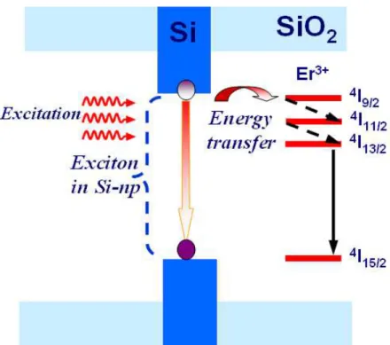
Figure 1.4: Illustration of energy transfer from Si-nps to Er3+ ions.
The interaction mechanism can be described as shown in figure 1.4. The recombination of exciton in the Si-nps is at the origin of the excitation of the Er3+ ions. The energy transfer occurring from the Si-nps towards the Er3+ ions leads to the excitation of the 4f electrons from the ground level of the Er (4I15/2) to the excited
states (4I13/2, 4I11/2, and 4I9/2). Then two deexcitation steps, 4I9/2→ 4I11/2 and 4I11/2→ 4
I13/2, occurs in a non-radiative way and in characteristic times[50] of about few 100 ns.
And finally the excitons in 4I13/2 level recombine radiatively to the ground level
emitting a photon at 0.98 and 1.54 µm corresponding to the transitions 4I11/2→ 4I15/2
and 4I13/2→ 4I15/2, respectively.
1.2.2 Fabrication
The fabrication of Si-based films co-doped by Si-nps and Er ions concerns many technologies. For examples, ion implantation of fused silica[47] [ 51 ] [ 52 ] allows obtaining SRSO layers having a Si excess ranging from 5 to 15 at.%. These films are then annealed to form and grow Si-nps in host matrix. This step is followed by Er implantation with different Er ion contents ranging from 2×10¹⁹ to 6×1020 cm-3. Some works carry out only one step of Er implantation into the SRSO films, which are deposited by PECVD[53][54]. A more direct approach is a co-incorporation of both Er
15
ions and Si excess during the deposition of Si-based layer as shown in the case of PECVD[55], co-evaporation[56] or magnetron co-sputtering[57] techniques. The PECVD method consists in plasma dissociation of silane, nitrous oxide and a volatile erbium organic chelate in a parallel-plate plasma chamber. The film stoichiometry is controlled by varying the relative flow rates of the reacting gases, and by monitoring both the temperature of organic precursor and the flow rate of the gas. The co-evaporation method is based on simultaneous evaporation of SiO powder from a thermal cell, SiO2 powder from an electron beam gun, and Er from an effusion cell.
The power of the evaporation sources is adjusted accordingly to obtain the desired sample composition. The magnetron co-sputtering technique consists in sputtering simultaneously Si, SiO2, and Er2O3 targets in pure Ar plasma. The RF power applied
on each cathode allows controlling the Si excess and Er content incorporated in the growing layer. This deposition technique permits also to grow Er-doped nitride layer by co-sputtering Si and Er2O3 targets in Nitrogen-rich plasma[17]. Magnetron
sputtering deposition has been used in this thesis work and will be described in detail in the chapter 2.
1.2.3 Optical properties
(a) PhotoluminescenceThe demonstration of the efficient energy transfer from Si-nps to Er3+ ions is shown in figure 1.5(a). With the increasing of Er content incorporated into the SiO2
matrix, the PL peak intensity of Si-nps gradually decreases while the 1.54µm-Er PL peak increases[58]. The characteristic distance for effective interaction between Si-nps and Er3+ ions is less than about 0.5 nm[59] [60], and the interaction coefficient is a decreasing exponential with increasing Si-np:Er3+ distance[ 61 ]. Consequently, the critical points to achieve an intense IR emission are the Si-nps density and the Er3+ ions concentration. Hijazi et al.[62] have optimized the coupling between Si-based sensitizers and Er3+ ions via tuning both the Er content and Si excess incorporated in SRSO matrix. They achieved the maximum Er3+ PL intensity corresponding to the films containing 3.5×1020 cm-3 Er atoms and 9 at.% Si excess. Numerous works[63][64]
[65]
focus on samples annealed at low temperatures (in the 700-900°C range), because higher temperature would result in a coalescence phenomenon of sensitizers and/or
16
Er3+ ions. Moreover, these low annealing temperature processes have allowed to demonstrate that the physics of transfer mechanism does not depend on the Si-np nature (crystalline or amorphous)[61]. For low annealing temperature, other kinds of sensitizers have been reported:
• the luminescence centers (LCs)[66]
• the atomic scale Si sensitizers[67]
• the Si oxygen deficient centers (SiODCs)[68].
In the case of SRSN host matrix, similar Er3+ PL intensities are observed by Yerci et al[69] across a large range of Si concentration from 0 to 12.5 at.%. The Er3+ PL emission has been optimized after an annealing treatment at 800°C during 200 seconds. Some results support the quantum confined Si-nps acting as sensitizer for Er3+ ions[70], whereas some others claim that the band tail states are at the origin of the sensitization of Er3+ ions[71][72].
Figure 1.5: (a) PL spectra of Si nanocrystal-doped SiO2 containing different Er
content in the range of 0-1.8 at.%[58], and (b) decay curves of Si nanocrystal dependence on Er content[60].
(b) Decay time
With increasing Er content, Watanable et al.[60] have evidenced a shortening of the Si-nps radiative decay time (Fig. 1.5(b)) which is a signature of the increasing number of Er ions coupled to Si-nps. Depending on the nature of the matrix (silicon oxide or nitride), the fabrication process and annealing step, the lifetime of the
17
I13/2-I15/2 transition is ranging from about 1 ms[54] up to 9 ms[5]. In the case of SRSO
matrix, its value shows a drastic reduction from 3.7 to 1.5 ms as the Si excess is increased from 3 to 4 at.%[ 73 ]. The same trend has been reported in the case of increasing Er content[74]. In contrast, longer annealing duration up to 1 hour at 800°C favors longer Er3+ lifetime[75]. In the case of SRSN host matrix, similar evolution of Er3+ lifetime is reported with a decrease from 3.2 to 1.4 ms when Si excess is varying from 0 to 17 at.%[73]. Recently, Steveler et al.[76] show that the Er3+ lifetime varies from about 0.9 to 1.4 ms when annealing temperature is ranging from 600 to 1100°C.
Optimum luminescence properties, i.e. strong luminescence intensity and decay time close to maximum theoretical limit, are the result of two compromises. First, the silicon excess should be important but below a threshold above which the amount of defects created induces too many non-radiative de-excitation pathways. Second, a significant content of rare earth ions is needed but it should be below a threshold beyond which cross relaxations begin, decreasing the global luminescence efficiency.
1.2.4 Devices
The indirect excitation of Er3+ ions by Si-nps in Si-based films provides promising potential as an active medium for compact and low cost devices, such as optical amplifier, light emitting diodes (LEDs), or laser. The most advanced demonstration highlighting the advantage of Si-nps sensitizing for Er3+ ions is a rid waveguide amplifier based on the Si-based film, which is pumped by low-cost LEDs as shown in figure 1.6[77]. As the Si-based films are transparent and have higher refractive index than that of SiO2, light can be confined and transmitted along the film
acting as a core of waveguide. The pumping light is absorbed by Si-nps which transfer their energy to Er3+ ions. The signal propagating in such a waveguide is amplified through stimulated emission of Er3+ ions.
18
Figure 1.6: Waveguide amplifier based on co-doped of Si-nps and Er in Si-based film adopting vertical pump sources supplied by low-cost LEDs.
Nevertheless, there are many processes that can compete with the transfer mechanism between Si-nps and Er3+ ions, generating extra pump power dependent losses or increasing the pump threshold necessary for population inversion of Er3+ ions. For Si-nps, the exciton recombination rate is increased through Auger process[78] while carrier absorption phenomenon leads to a decrease of excitons available for energy transfer to rare earth ions[79]. In the case of Er3+ ions, several processes are responsible of Er3+ emission quenching: (i) excited state absorption in an Er3+ ion[80], (ii) energy migration and cross relaxation between Er3+ ions[ 81 ], (iii) cooperative up-conversion between excited Er3+ ions[82], and (iv) the energy back transfer from Er3+ ions to Si-nps[83]. These issues really prevent the achievement of net gain and the realization of effective light source of Er-doped Si-based materials[84].
1.3 Nd and Si nanostructure
1.3.1 Introduction
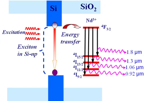
Nd3+ ion has also a resonant energy level with the bottom of the conduction band of the Si-nps and therefore has been the subject of some interest[85]. This ion has two interesting emission wavelengths as shown in figure 1.7:
19
● The 1.064 µm emission which has been widely used for laser when Nd ions are incorporated in a YAG crystal. The application domains are etching, cleaning (matrices, art objects) or medicine fields (elimination of the membranes, treatment of skin cancers and removing of lithiases in body).
● The 1.3 µm emission which is slightly absorbed by the silica fiber (~0.3 dB.km-1) and therefore is interesting for optical telecommunication in O-band.
Figure 1.7: Illustration of energy transfer from Si-nps to Nd3+ ions.
In Si-Nd3+ system, the same interaction process described in the case of Er3+ ions (cf section §1.2.1) occurs. The exciton generated inside the Si-nps by the absorption of a photon recombines non-radiatively by exciting a Nd3+ ion in 4F3/2 level via a
dipole-dipole interaction (seen Fig. 1.7). From 4F3/2 level four radiative transitions
occurs leading to four emission wavelengths at 1.8, 1.3, 1.06, and 0.92 µm corresponding to the 4F3/2→ 4I15/2, 4F3/2→ 4I13/2, 4F3/2→ 4I11/2, and 4F3/2→ 4I9/2
deexcitation, respectively. Their relative emission intensities vary and are described by the different transition rates which are about 10, 300, 1460, and 1280 s-1, respectively[86][87][88].
As in the case of Er3+ ions, the energy transfer time is very short (about 150 ns)[89], which favors the excitons within Si-nps to preferably sensitize Nd3+ ions rather than to radiatively recombine. Size of Si-nps plays an important role in the
20
sensitization process. Thus, Watanable et al.[90] have demonstrated that the increase in the Si-nps size from 2.7 to 3.8 nm results in a decreasing of Nd3+ PL intensity. They concluded that only small Si-nps can excite the 4F3/2 level of Nd3+ ions.
1.3.2 Nd-doped Matrices
(a) SiOx matrixA SiOx or called also SRSO (Si-rich Silicon Oxide) is a non-stoichiometric
material, which can be considered as an oxygen- deficient SiO2. The co-incorporation
of Si excess and Nd ion allows the formation of Si-np that can be optically coupled to Nd3+. In order to optimize such coupling, two main ways have been investigated:
• The film composition engineered by the deposition conditions. Nd content is one important factor. MacDonald et al.[89] have varied the Nd content from 0.19 to 1.29 at.% in co-evaporated films and obtained a maximum PL intensity corresponding to the 0.29 at.%. In reactive sputtered layers, this maximum value has been found to be lower than 0.1 at.%[ 91 ]. They both demonstrated that the high Nd content would decrease the amount of optically active Nd3+ ions and/or form Nd2O3
clusters leading to cross relaxation between Nd ions. Si excess is the other key parameter to maximize the Si-np:Nd3+ coupling number. High Si-nps density is needed but a high Si excess favors the non-radiative pathways as detailed in the case of the Er ions. For example, the maximum PL intensity of Nd3+ ions at 1.064 µm corresponds to 5.6 at.% Si excess reported by S-Y. Seo et al.[92].
• The film microstructure monitored by the post-annealing process. During annealing treatment, a phase separation occurs allowing the growth of Si-nps[93]. The duration and temperature have to be controlled to permit an optimized distribution of Si-nps and therefore a high sensitizer density. Concerning the Nd ions, this step is of importance too because it favors the optical activation of Nd3+ ions but a too high temperature may induce the formation of Nd clusters[ 94 ]. Bréard et al.[ 95 ] have evidenced the presence of two decay times in their PL experiments (Fig. 1.8): (i) a fast decay component in the range of 5 to 50 µs attributed to Nd2O3 clusters
21
and (ii) a slow decay component ranging from 50 to 170 µs originating from isolated Nd3+ ions.
Figure 1.8: Nd3+ concentration dependence of lifetimes[95] both for 0. 92-µm-Nd3+ PL fitted by two exponential laws. The inset shows its typical decay curve with fitting line. (b) SiNx matrix
SiNx matrix is derivate from stoichiometric Si nitride (Si3N4) in which x=1.33.
When x<1.33 Si atoms are incorporated into Si3N4 and the matrix is generally called
Si-rich Silicon Nitride (SRSN).
Contrarily to the Er doped nitride system, only a few papers report optical properties of Nd-SRSN system one. Li et al.[94] have studied the evolution of Nd3+ PL intensity as a function Si excess (x ranging from 1.27 to 1.04). They have evidenced a dramatic decrease of Nd3+ emission with the increasing Si excess. Such an evolution is explained by the decrease of band gap as well as the density of localized defects states that act as sensitizers towards the Nd3+ ions. For larger Si excess (x=0.6), Biggemann et al.[ 96 ] observed the maximum Nd3+ PL efficiency corresponding to matrix band gap, which is twice the 4F3/2 → 4I9/2 transition energy. These authors
evidenced an efficient sensitization of the Nd3+ ions by the presence of localized defect state in the band gap. The maximum Nd3+ PL intensity has been achieved for a concentration of 3×10²⁰ at.cm-3[94]. As in the case of SiOx matrix, higher Nd content
22
leads to the formation of Nd2O3 clusters. The 4F3/2 → 4I11/2 decay time of Nd3+ PL in
this SRSN matrix has a two exponential feature with a fast (50 µs) and slow (140 µs) lifetimes[94].
1.3.3 Devices
Once effective light emission in optical fiber was achieved from Nd3+ ions doped in Si-based materials, this provided an alternative way to solve limiting factors previously mentioned in the case of Er3+ doping. Several results have been found to inspire and motivate researchers. In the case of SiOx matrix, Rebohle et al.[97] have
clearly observed the electroluminescence peak from Nd3+ ions. In the case of SiNx
matrix, an optical gain of 270 cm-1 at 1130 nm has been determined from the planar waveguides excited by non-resonant wavelength with Nd3+ transitions[98]. And Li et al.[94] have fabricated an active micro-disk resonator radiatively emitting 1.1 µm by stimulation mechanism.
1.4 Conclusion:
A review of Si-based light emission has been performed in this chapter concluding that the important potential applications of Si photonics have driven an increasing interest on the Si-based materials doped by Er3+ rare earth ions. An achievement of net gain from Er3+ ions has been hampered as mentioned above by several critically limited factors such as excited state absorption, energy migration, cross relaxation, and cooperative up-conversion. Moreover, the nature of the three-level electronic 4f structure of Er3+ ions is a detrimental feature which leads to the re-absorption of the 1.54 µm emitted light. In contrast, Nd3+ ions have four-level structure, for the emission at 1.06µm, favoring the achievement of a large population inversion. Consequently, such a system could be promising for the fabrication of a net gain Si-based amplifier.
Nevertheless, Nd-doped Si-based system presents some limitations that can be detrimental for getting an efficient device. To enhance the PL properties of Nd-doped layers, Nd content and Si excess should be optimized. On one hand, a high Nd concentration favors the energy migration and cross relaxation, as well as formation Nd2O3 clusters. One the other hand, a high Si-nps density required for decreasing the
23
Si:Nd distance, would lead to the decrease of the Nd3+ decay time (the order of µs). These different limiting factors are serious drawbacks for sensitization of rare earth ions by Si-nps in Nd-doped Si-based films and thus the breakthroughs are required for the achievement of Si photonics devices.
This is the objective of this work. We proposed to improve by a fine tuning of the fabrication and/or annealing conditions, the microstructure of the layers and to maximize of both Si-nps and Nd3+ ions density, to reach Nd3+ population inversion and gain. The PhD work has been done within the ANR DAPHNES project (ANR-08-NANO-005).
24
Bibliography
[1] L. T. Canham, Appl. Phys. Lett. 57 1046 (1990)
[2] B. Jalali, http://www.aps.org/publications/apsnews/200603/forefronts.cfm, [3] U. Gnutzmann , K. Clausecker, Appl. Phys. 3 (1974) 9
[4] L. E. Brus, J. Chem. Phys. 79 (1983) 5566
[5] J. P. Wilcoxon, G. A. Samara, P. N. Provencio, Phys. Rev. B 60 (1999) 2704 [6] N. M. Park, C. J. Choi, T. Y. Seong, S. J. Park, Phys. Rev. Lett. 86 (2001) 1355 [7] H. Rinnert, M. Vergnat, G. Marchal, A. Burneau, J. Lumin. 80 (1999) 445
[8] M. Zacharias, J. Heitmann, R. Scholz, U. Kahler, M. Schmidt, J. Blasing, Appl. Phys. Lett. 80 (2002) 661
[9] X.Y. Chen, Y.F. Lu, Y.H. Wu, B.J. Cho, W.D. Song, D.Y. Dai, J. Appl. Phys. 96, (2004) 3180
[10] S. Guha, M. D. Pace, D. N. Dunn, I. L. Singer, Appl. Phys. Lett. 70 (1997) 1207 [11] Z. H. Lu, D. J. Lockwood, J.M. Baribeau, Nature, 378 (1995) 258
[12] F. Iacona, G. Franzò, and C. Spinella, J. Appl. Phys. 87 (2000)1295
[13] L. Y. Chen, W. H. Chen, and F.C. N. Hong, Appl. Phys. Lett. 86 (2005)193506 [14] L. B. Ma, R. Song, Y. M. Miao, C. R. Li, Y. Q. Wang, Z. X. Cao, Appl. Phys. Lett.
88 (2006) 093102
[15] L. F. Bian, C. G. Zhang, W. D. Chen, C. C. Hsu, Y. H. Qu, D. S. Jiang, J. Appl. Phys. 99 (2006) 094302
[16] R. Nalini, L. Khomenkova, O. Debieu, J. Cardin, C. Dufour, M. Carrada, F. Gourbilleau, Nanoscale Res. Lett. 7 (2012)124
[17] S. Cueff, C. Labbé, L. Khomenkova, O. Jambois, P. Pellegrino, B. Garrido, C. Frilay, R. Rizk, Mater. Sci. Eng. B 177 (2012) 725
[18] M. Wang, D. Li, Z. Yuan, D. Yang, D. Que, Appl. Phys. Lett. 90 (2007) 131903 [19] L. Khomenkova, F. Gourbilleau, J. Cardin, O. Jambois, B. Garrido, R. Rizk, J. Lumin. 129 (2009) 1519
[20] W. Pan, R. G. Dunn, M. S. Carroll, J. C. Banks, L. N. Brewer, J.Non-Cryst. Solids 354 (2008) 975
[21] R. Pratibha Nalini, C. Dufour, J. Cardin, F. Gourbilleau, Nanoscale Res. Lett. 6 (2011) 156
[22] E. Quiroga-González, W. Bensch, M. Aceves-Mijares, Z. Yu, R. López-Estopier, K. Monfil-Leyva, Thin Solid Films, 519 (2011) 8030
[23] B. G. Fernandez, M. Lopez, C. Garcia, A. Perez-Rodriguez, J. R. Morante, C. Bonafos, M. Carrada, A. Claverie, J. Appl. Phys. 91 (2002) 798
[24] I. Stenger, B. Gallas, L. Siozade, C. C. Kao, S. Chenot, S. Fisson, G. Vuye, J. Rivory, J. Appl. Phys. 103 (2008) 114303
25
[25] P. R. Wilson, T. Roschuk, K. Dunn, E. N. Normand, E. Chelomentsev, O. H. Zalloum, J. Wojcik, P. Mascher, Nanoscale Res. Lett. 6 (2011) 168
[26] T. Inokuma, Y. Wakayama, T. Muramoto, R. Aoki, Y. Kurata, S. Hasegawa, J. Appl. Phys. 83 (1998) 2228
[27] D. Kovalev, J. Diener, H. Heckler, G. Polisski, N. Künzner, F. Koch, Phys. Rev. B 61, (2000) 4485
[28] C. Lecerf, Elaboration et caractérisations de films d'oxyde de gallium dopés terres rares, PhD thesis, Universite de caen/Basse-Normandie, (2011)
[29] M. S. Yang, K. S. Cho, J. H. Jhe, S. Y. Seo, J. H. Shin, K. J. Kim, D. W. Moon, Appl. Phys. Lett. 85 3408 (2004)
[30] L.V. Mercaldo, P.D. Veneri, E. Esposito, E. Massera, I. Usatii, C. Privato, Mater. Sci. Eng. B 159 (2009) 77
[31] J. Kistner, X. Chen, Y. Weng, H.P. Strunk, M.B. Schubert, J. H. Werner, J. Appl. Phys. 110 (2011) 023520
[32] G. R. Lin, C. J. Lin, J. Appl. Phys. 95 (2004) 8484
[33] Y. C. Fang, Z. J. Zhang, M. Lu, J. Lumin. 126 (2007) 145
[34] M. Wang, D. Yang, D. Li, Z. Yuan, D. Que, J. Appl. Phys. 101 (2007) 103504 [35] M. V. Wolkin, J. Jorne, P. M. Fauchet, G. Allan, C. Delerue, Phys. Rev. Lett. 82 (1999) 197.
[36] G. Allan, C. Delerue, M. Lannoo, Phys. Rev. Lett.78 (1997) 3161
[37] G. Zatryb, A. Podhorodecki, J. Misiewicz, J. Cardin, F. Gourbilleau, Nanoscale Res. Lett. 6 (2011) 106
[38] M. Dovrat, Y. Goshen, J. Jedrzejewski, I. Balberg, A. Sa’ar, Phys. Rev. B 69 (2004) 155311
[39] R. J. Walters, J. Kalkman, A. Polman, H. A. Atwater, M. J.A. de Dood, Phys. Rev. B 73 (2006) 132302
[40] M.L. Brongersma, A. Polman, K.S. Min, E. Boer, T. Tambo, H.A. Atwater, Appl. Phys. Lett. 72 (1998) 2577
[41] L. Dal Negro, J. H. Yi, L. C. Kimerling, S. Hamel, A. Williamson, and G. Galli, Appl. Phys. Lett. 88 183103 (2006)
[42] M. Wang, M. Xie, L. Ferraioli, Z. Yuan, D. Li, D. Yang, and L. Pavesi, J. Appl. Phys. 104 083504 (2008)
[43] L. Pavesi, L. D. Negro, C. Mazzoleni, G. Franzo, F. Priolo, Nature 408 (2000) 440
[44] O. Boyraz, B. Jalali, Opt. Express 12 (2004) 5269.
[45] H. Rong, A. Liu, R. Jones, O. Cohen, D. Hak, R. Nicolaescu, A. Fang, M. Paniccia, Nature 433 (2005) 292.
[46] A.J. Kenyon, P.F. Trwoga, M. Federighi, C.W. Pitt, J. Phys.: Condens. Matter 6 (1994) L319


![[PDF] Formation informatique Xhtml en pdf](data:image/gif;base64,R0lGODlhAQABAIAAAP///wAAACH5BAEAAAAALAAAAAABAAEAAAICRAEAOw==)