HAL Id: hal-00575828
https://hal-iogs.archives-ouvertes.fr/hal-00575828
Submitted on 6 Apr 2012
HAL is a multi-disciplinary open access
archive for the deposit and dissemination of
sci-entific research documents, whether they are
pub-lished or not. The documents may come from
teaching and research institutions in France or
abroad, or from public or private research centers.
L’archive ouverte pluridisciplinaire HAL, est
destinée au dépôt et à la diffusion de documents
scientifiques de niveau recherche, publiés ou non,
émanant des établissements d’enseignement et de
recherche français ou étrangers, des laboratoires
publics ou privés.
Nanometric deformations of thin Nb layers under a
strong electric field using soft x-ray laser interferometry
Gérard Jamelot, David Ros, A. Carillon, Bedrich Rus, T. Mocek, M. Kozlova,
A.R Prag, Denis Joyeux, Daniel Phalippou, M. Boussoukaya, et al.
To cite this version:
Gérard Jamelot, David Ros, A. Carillon, Bedrich Rus, T. Mocek, et al.. Nanometric deformations of
thin Nb layers under a strong electric field using soft x-ray laser interferometry. Journal of Applied
Physics, American Institute of Physics, 2005, 98 (4), pp.044308 - 044308-7. �10.1063/1.2010620�.
�hal-00575828�
Nanometric deformations of thin Nb layers under a strong electric field
using soft x-ray laser interferometry
G. Jamelot, D. Ros, A. Carillon, B. Rus, T. Mocek et al.
Citation: J. Appl. Phys. 98, 044308 (2005); doi: 10.1063/1.2010620 View online: http://dx.doi.org/10.1063/1.2010620
View Table of Contents: http://jap.aip.org/resource/1/JAPIAU/v98/i4 Published by the American Institute of Physics.
Additional information on J. Appl. Phys.
Journal Homepage: http://jap.aip.org/
Journal Information: http://jap.aip.org/about/about_the_journal Top downloads: http://jap.aip.org/features/most_downloaded Information for Authors: http://jap.aip.org/authors
Nanometric deformations of thin Nb layers under a strong electric field
using soft x-ray laser interferometry
G. Jamelot,a兲 D. Ros, and A. Carillon
Laboratoire d’Interaction du rayonnement X Avec la Matière, Unite Mixte de Recherche (UMR) n° 8624, Université Paris-Sud and Centre National de la Recherche Scientifique (CNRS), Bâtiment 350,
91405 Orsay, France
B. Rus, T. Mocek, M. Kozlová, and A. R. Präg
Department of X-ray Lasers, Institute of Physics/Prague Astrix Laser System (PALS) Research Centre, 18221 Prague 8, Czech Republic
D. Joyeux and D. Phalippou
Laboratoire Charles Fabry de l’Institut d’Optique, Bâtiment 503, 91403 Orsay, France M. Boussoukaya, M. Kalmykow, F. Ballester, and E. Jacques
Service d’Etude des Accélérateurs, Commissariat à l’Energie Atomique, Centre d’Etudes Nucléaires de Saclay, 91191 Gif sur Yvette, France
共Received 28 February 2005; accepted 11 July 2005; published online 18 August 2005兲
We present measurements of in situ nanometric-resolution topographical modifications of thin niobium layers subjected to strong electric fields. The Nb layers, deposited on a fused silica substrate, are interferometrically flash probed using soft x-ray laser 共XRL兲 at the wavelength of 21.2 nm. Its pulses are reflected by the probed sample under grazing incidence angle, and the information about surface deformation is obtained by a Fresnel wave-front-division interferometer. It was experimentally established that the probing pulses at the soft x-ray wavelength do neither produce any measurable photoelectric-field emission, nor alter the topographical features of the probed surface. The examined Nb electrodes were periodically probed while the electric field was increased up to 80 MV/ m, and alterations of their topographical characteristics with a resolution of
⬃2 nm in the relief elevation were obtained. It was found that behavior of the Nb layer strongly
depends on the polarity of the applied voltage. Only small modifications are observed with the Nb surface at the positive potential, whereas the negative potential induces significant transient surface perturbations, with peak-to-valley elevation differences ⬃50 nm. The qualitative nature of these modifications was observed to be unrelated to intermittent parasitic breakdowns. © 2005 American
Institute of Physics.关DOI: 10.1063/1.2010620兴
I. INTRODUCTION
Metallic surfaces submitted to intense electric fields emit electrons.1,2While significant field emission, resulting in ap-preciable current for cathodes of approximately cm2 size, is
theoretically expected to occur typically at electric fields to the order of GV/m, large emission currents are experimen-tally detected at much lower-field strengths. This field emis-sion limits the attainable value of the applied electric field, which is a serious limitation for building superconducting linear accelerators and colliders 共such as teraelectron volt energy superconducting linear accelerator 共TESLA兲, with a goal to produce beam energy of 1 TeV兲, namely, of its in-jecting devices based on rf cavities.3The field-emitted elec-trons impact on the cavity surface, leading to its heating and consequently increasing its electrical resistance. In an ex-treme case, field emission of the cavity walls can lead to thermal breakdown. The field emission and the below-threshold breakdowns phenomena limit rf electric fields in the present experimental superconducting structures to val-ues between 15 and 20 MV/ m and lead to significant addi-tional costs to reach the projected parameters.
To understand the detrimental effects of field emission, it is imperative to determine to which extent the dissipative phenomena are related to the nature of the sample, or whether they originate in external elements due to the fabri-cation process.4
Scanning electron microscopy5 and scanning tunneling microscopy6 have shown links between field emission and surface contaminants and/or minute surface defects. How-ever, these diagnostics provide information about the surface only after its exposure to the electric field is terminated共the rf cavity is cut apart to allow examination兲, hence do not allow visualization during the field emission, or accessing surface alterations ahead of the breakdown. High-resolution
in situ thermometry, using an array of temperature sensors,
has been used to provide the heat patterns due to impacting electrons originated from a field emitter, e.g., in rf niobium cavity at 1.6 K.7 While it is possible with this technique to localize some field-emission sites, the field emitters exhibit rather complex morphology, and no information is provided about the surface before the electrons are emitted.
Interferometry using soft x-ray laser pulses offers quali-tatively an alternative technique of in situ surface mapping, able to distinguish nanometric altitude features at the same
a兲Electronic mail: [email protected]
JOURNAL OF APPLIED PHYSICS 98, 044308共2005兲
time as the electron emission occurs. It was demonstrated in our earlier work,8in which it was applied to visualization of modifications of a surface of bulk niobium, subjected to elec-tric field. In addition to nanometer altitude resolution capa-bility due to the wavelength, a major advantage of soft x-ray and interferometry is that the probing electromagnetic wave totally reflects off a metallic surface when incident at small grazing angle, since the real part of the refraction index 共n = 1 −␦− i兲 for x rays is less than 1. In contrast with the case of visible or UV light, the frequency of the incident soft x-ray wave is higher than the plasma frequency of a metal, and the mechanisms of reflection qualitatively differ as a result. Due to the comparably low optical frequency, the vis-ible or UV light, incident on a metallic surface under a strong electric bias field, will likely affect the electron field emis-sion. The optical wave induces on the metal a resonant sur-face current, which, in conjunction with the associated large magnetic field of the penetrating damped wave,9 is capable to produce field enhancement on microscopic imperfections of the surface共see, e.g., Ref. 4兲. This problem is dramatically reduced for soft x rays with its frequency above the metal plasma frequency, since the amplitudes of the induced sur-face current and of the associated magnetic field are much smaller.
On the other hand, the critical angle of niobium, at the wavelength of 21.2 nm of the soft x-ray laser employed, is c= 37.5°共measured up from the surface兲. A beam incident at
a grazing angle of 6° will produce evanescent wave with a penetration depth of only 2.7 nm.10Also, in this experiment, the probing soft x-ray beam is s polarized when incident on the Nb cathode, which further decreases the penetration depth inside the investigated surface.
The XUV interferometry of nonstationary surfaces re-quires monochromatic-pulsed sources of high brightness. Synchrotron radiation is therefore not suitable, since it calls for rather long exposure times. In contrast, x-ray lasers pro-vide an ideal radiation source due to their short pulse
共⬍100 ps兲, delivered in a narrowly collimated and highly
coherent beam. This makes it possible to probe the examined surface in a snapshot and to visualize, with nanometric alti-tude resolution, transient surface alterations inaccessible by other techniques.
In this paper we present results of investigation of the behavior of thin Nb layers deposited on fused silica sub-strates, subjected to fields up to 80 MV/ m, with both posi-tive and negaposi-tive polarities.
II. EXPERIMENTAL SETUP
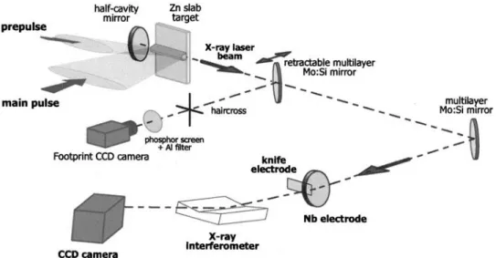
The experiment was performed at the PALS共Prague As-terix Laser System兲 facility,11 using its iodine IR laser to pump a plasma-based soft x-ray laser emitting at the wave-length of 21.2 nm. A schematic view of the experimental arrangement is shown in Fig. 1. The x-ray laser is generated on the surface of a zinc slab, by a pump sequence consisting of a weak共⬃2 J兲 prepulse, followed after 10 ns by the main pulse delivering ⬃500 J of net energy. The x-ray laser
共XRL兲 beam emerging from the amplifying plasma may be
detected either as a “footprint” via a flat retractable Mo:Si multilayer mirror or sent by another multilayer mirror to-wards the x-ray interferometer, reflecting on its path off the probed Nb surface. The multilayer mirrors operate at an in-cidence angle of 45° and besides acting as a cut-off filter for keV x-ray and UV emissions, they work as soft x-ray polar-izers, since 45° incidence angle approximately corresponds to the Brewster’s angle.12The reflected XRL beam is conse-quently s polarized共electric vector parallel to the polarizer兲.
A. X-ray laser
The soft x-ray laser operated at PALS共Ref. 13兲 provides strongly amplified emission at 21.2 nm, corresponding to the
J = 0 – 1 transition 共2p1/25 3p1/2兲J=0→共2p1/2 5 3s
1/2兲J=0 in
neon-like zinc. It operates in double-pass regime, employing a 3 -cm-long plasma and flat half-cavity Mo:Si multilayer mirror located 8.5 mm from the plasma end. The prepulse and the main pumping pulse have both duration of⬃400 ps and
gen-FIG. 1. Experimental arrangement of the soft x-ray laser and the interferometric arm共not to scale兲. The XRL beam is switched between the footprint monitor and the interferometer by a retractable multilayer mirror working at 45°. Another multilayer mirror at 45° sends the beam to the interferometer, polarizing it vertically.
erate x-ray lasing action in the “quasistationary state”共QSS兲 regime, which is characteristic by a high output energy but requires relatively large pump device. Here, the deeply satu-rated double-pass XRL beam provides ⬃4 mJ of energy in
⬇80-ps pulses, corresponding to a peak power in excess of
40 MW. The x-ray laser shot at the PALS facility may be fired every 20 min.
The amplifying plasma column is generated in a regime in which the main pulse, producing net target irradiance of
⬃2.8⫻1013Wcm−2, is focused significantly more tightly
共⬃130m兲 than the prepulse 共⬃700m兲. In conjunction with the half cavity and a uniform main pulse focus gener-ated by a composite lens matrix,14this arrangement produces an XRL beam exhibiting a high spatial quality as well as excellent shot-to-shot reproducibility; the respective horizon-tal and vertical divergences of the beam are ⬃4 and
⬃6 mrad.
B. Niobium electrodes and electrical circuit
The Nb electrodes used in this work were deposited by ion-beam magnetron sputtering on 15-mm-diameter super-polished, fused silica substrates with rms surface roughness of ⬃15 Å. The thickness of the Nb layer is about 0.5m. The working potential of such a layer is approximately equal to 4.3 eV that of bulk Nb. The samples were kept under neutral atmosphere 共N2兲 until the moment of their
installa-tion into the vacuum chamber. The experiment was per-formed under vacuum of about 10−6Torr at room tempera-ture.
The second electrode was constituted by a thin iron knife
共see Fig. 1兲, 10 mm large and 600m thick. Its distance from the Nb surface, which was typically 1 mm, as well as its parallelism with this surface, was carefully adjusted.
Figure 2 shows the geometry under which the Nb layers were probed by the XRL beam. The beam is incident on the surface under a grazing angle of 6°, which is significantly smaller than the critical angle of 37.5° for the 21.2-nm ra-diation, and makes the niobium about 90% reflective for s polarization at this wavelength. As mentioned earlier, the evanescent wave associated with the reflected XRL beam and penetrating into the layer is very weak.
As seen from Fig. 2, the knife-edge electrode is placed asymmetrically with respect to the substrate center, about 3.5 mm to one side. Thus the first half of the XRL beam provides, upon reflection off the unperturbed Nb surface, the
reference wave front, whereas the second half of the beam carries information about the deformed surface underneath the knife electrode.
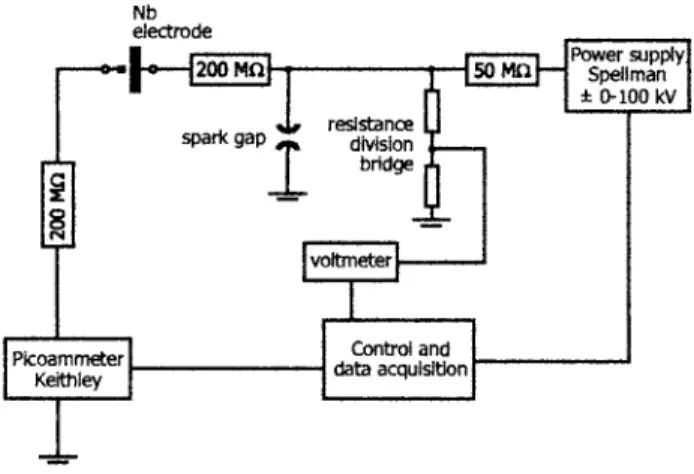
The setup of the employed high-voltage共HV兲 electrical circuit is shown in Fig. 3. The circuit produces dc electric field with amplitudes on the Nb surface from 0 to 100 MV/ m. The electric current passing by the sample is measured each 300 ms by a picoammeter which integers the charge over 80 ps. A spark gap protects the picoammeter against high electric currents due to possible breakup and breakdown. The measurements were made with both polari-ties. In the first case, the Nb layer was at the negative poten-tial and acted as electron emitter. In the second case, the Nb layer was at the positive potential and acted as electron col-lector.
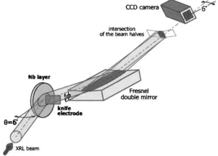
C. X-ray interferometer
The device employed to analyze the wave front of the x-ray beam reflected off the probed Nb surface is a Fresnel bimirror interferometer.15,16It belongs to the class of wave-front-division interferometers and constitutes a versatile tool utilizable over a wide spectral range in the x-ray and XUV domain. Due to its robustness and simple alignment, it may be easily employed in conjunction with an x-ray laser,17 con-stituting an alternative to amplitude-division devices.18,19 Compared to the other prototype of wave-front-division in-terferometer, namely, the Lloyd mirror,20 the Fresnel bimir-ror presents two decisive advantages. First, the separation of any pair of interfering rays is constant across the field, thus avoiding fringe modulations from spatial coherence issues. Second, the fringe spacing is independent of the beam inci-dence onto the bimirror, while in the Lloyd case, inciinci-dence must be kept highly grazing, which makes fringe adjustment much more tricky.
The geometry of the interferometer and a scheme of its implementation in the experiment are shown in Fig. 4. The interferometer consists of a tandem of adjacent high-quality plane mirrors 15⫻60 mm2, inclined to each other at a small
angle共5.2 mrad兲 and fixed on a common support. The x-ray beam reflected off the Nb cathode is incident on the tandem of mirrors in the plane of symmetry of the system, containing the line along which the mirrors join. Upon reflection, the
FIG. 2. Schematic of the niobium-coated flat substrate and an iron knife electrode system, showing the principle of the probing technique共not to scale兲.
FIG. 3. Setup of the HV electric circuit. Both positive and negative voltages up to 100 kV may be applied to the system Nb electrode-knife edge.
beam is split up vertically, with respect to the plane of inci-dence, into two halves. The beam halves propagate with a small angle toward each other and produce interference pat-tern as they overlap. It may be easily shown that for a par-allel beam, the fringe period equals/共2兲, whereis the grazing angle of incidence of the beam on the system 共mea-sured with respect to the central groove, see Fig. 4兲 and is the angle between the two mirrors. For a divergent XRL beam, emitted from a nearly point source, the fringe period is increased to 共/2兲D2/ D1, where D2 and D1 are,
respec-tively, the optical distances of the detector and of the Fresnel bimirror from the source. For =21.2 nm, = 6°, = 5.2 mrad, D1= 300 cm, and D2= 370 cm, the fringe period
is⬃24m.
The resulting interferograms were detected by a phosphor-coated 512⫻512 pixel 12-bit charge-coupled de-vice共CCD兲 camera 共ARP Photonetique兲 with an active sur-face of 10⫻10 mm2, located 70 cm downstream from the Fresnel bimirror. The camera was inclined to view the fringes under an angle of 6°共see Fig. 4兲, which is identical to that under which the x-ray laser beam probes the Nb elec-trode. The reason for this arrangement is twofold. First, it allows augmenting the detected fringe spacing by nearly one order of magnitude 共1/sin 6° =9.57兲 to ⬃230m. Sec-ondly, the camera thus “views” dimensionally undistorted image of the probed surface scale, without asymmetrical lon-gitudinal stretching.
In the interferometric records, the fringe position is re-lated to the altitude profile of the Nb electrode in actual lateral scale. In other words, the altitude profile is encoded into the phase of the cosine of the fringe pattern. The per-turbed region under the knife electrode extends approxi-mately through the center of the fringe pattern, along vertical direction. Given the angle of incidence = 6° of the XRL beam to the Nb electrode, a shift of one fringe corresponds to the elevation on the Nb surface equal to /共2 sin兲
⬇100 nm.
III. PROCESSING OF THE INTERFEROGRAMS
The detected fringe pattern carries in principle “com-plete” information about the probed Nb surface, i.e., about its minute relief features as well as about its reflectivity being a function of the local value of the complex index of refrac-tion. It theoretically constitutes a reflection hologram of the surface, with a tilted offset reference wave 共see, e.g., Ref. 21兲. However, the holographic information encoded in the recorded pattern is in reality severely degraded by a number of experimental constraints. These include the limited spatial resolution due to the phosphor grain, due to the fiber-optic taper transmitting the image to the CCD chip, and due to the pixel size共19⫻19m2兲. Other limitations come from small
shot-to-shot variations of the intensity profile of the x-ray laser beam and from presumably uneven intensity response of the phosphor over its surface. Accordingly, both high and very low spatial frequencies in the interferograms carry only little physical information and are not employable in the analysis. The processing technique employed is therefore based solely on detection of the frequency shift of the inter-ference fringes, rather than on holographic reconstruction.
The recorded interferograms are digitally processed by usual Fourier techniques using the fast Fourier transform al-gorithm. In summary, as the surface elevation is coded into phase modulation of a carrier 共the fringe pattern兲, a phase demodulation of that carrier must be performed. This is ob-tained in the spectral domain by frequency shifting one side band of the fringe pattern towards zero, then low-pass filter-ing the spectrum, and finally back Fourier transform to the space domain, to get the complex modulation function, am-plitude, and phase. As usual, phase unwrapping is required when the phase excursion is larger than 2. As it is well known, unwrapping becomes problematic when signal/noise ratio is not large enough, leading to unphysical phase maps. This is why the low-pass filtering step must be adjusted to the actual signal/noise ratio, so that the phase noise does not dominate over the signal. Finally, the phase map is converted straightforwardly into elevation map, through 2h sin/ =/ 2.
Since there is no imaging between the probed Nb plane and the detector, the spatial resolution 共along the surface兲 provided by the resulting image is limited by diffraction. Also, the tilt of the object and the observation planes with respect to the direction of propagation results in asymmetry in resolution along the horizontal and the vertical direction. It may be seen easily that the horizontal resolution is reduced by a factor of 1 / sin 6 ° = 9.57, with respect to the vertical resolution. This latter can be assessed by considering the characteristic period of fringes in the Fresnel diffraction pattern,22equal to
冑
D, where D is the propagation distance. In this approach, features in the normal object plane much smaller than冑
D/2 will be smeared by diffraction. WithD = 700 mm,
冑
D/2 amounts to ⬃60m; thus the resolu-tion along the Nb surface is 60m vertically⫻600m horizontally, i.e., about 32共h兲⫻3共v兲 pixels.The altitude resolution is limited by the phase noise in the fringe pattern. Therefore, we consider as a reasonable estimation the sigma of the phase fluctuations in phase
pro-FIG. 4. Fresnel bimirror interferometer, analyzing the x-ray beam reflected from the vertically orientated Nb cathode共not to scale兲; the probing XRL beam is vertically polarized. The cathode is located at a distance of ⬃300 cm from the XRL exit aperture and a few centimeters before the Fresnel bimirror; the optical distance between the bimirror and the CCD camera is 70 cm. The grazing incidence of the CCD is 6° in order to en-hance the apparent fringe shift.
files obtained from interferograms without electrical field. As this is roughly equal to 2/ 50, and keeping in mind that one fringe shift corresponds to an altitude change of 100 nm共see Sec. II兲, the altitude resolution is about 100/50=2 nm.
IV. EXPERIMENTAL RESULTS
In each of two series of the measurements, the first x-ray laser shot was carried out with zero voltage between the Nb layer and the knife electrode, in order to obtain the reference interferogram of unperturbed Nb surface. The electric field was then gradually increased by steps going along with the 20-min repetition rate of the x-ray laser; the field was main-tained at a given value between two successive shots and was raised to the next-higher level shortly before firing the sub-sequent XRL shot. Two series of shots were taken with Nb layer at the negative potential, and one series with Nb at the positive potential.
A. Nb layer at the negative potential-electron emitter
In this configuration, the applied dc electric field was raised by steps from 0 to 60 MV / m. The measured average current passing through the electrode system, originating in the field emission, is displayed in Fig. 5. A measurable current—hence field emission—first appeared at 20 MV/ m, amounting to 0.02 nA. This current increased to 0.46 nA while the applied field was risen 60 MV / m; these amplitudes imply that field emission of electrons from the Nb surface is rather fairly weak.
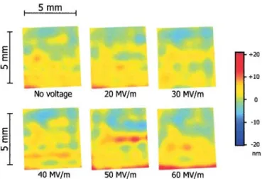
A sequence of x-ray interferograms recorded with the Nb layer at the negative dc potential up to 60 MV / m is shown in Fig. 6. It turns out that the individual records do not exhibit significant alteration of the fringe pattern with respect to the reference interferogram taken at zero field.
Figure 7 shows the reconstructed surface maps of the Nb layer, corresponding to the respective interferograms from Fig. 6. Up to 40 MV / m, only local surface elevations smaller than about 10 nm appear. At 50 MV / m, a horizontal ridge elevated by⬃15 nm above the adjacent surface is de-tected; this ridge is not observed in the subsequent shot taken at 60 MV/ m. We note that this feature, or other significant deviation from the plane surface, is not seen in the shots taken without electric field. This suggests that in this con-figuration the electric field produces small temporary elastic
deformations of the surface, which are apparently not con-nected to any permanent local characteristic of the Nb layer. In the course of this probing sequence, an accidental microdischarge occurred about 10 min after the XRL shot taken at 30 MV/ m, resulting in a short burst of the field-emission current of about 0.5A. As seen from Fig. 7, this microbreakdown does, however, not result in any palpable modification of the Nb surface—no additional systematic surface feature emerges from the records taken at 40 MV/ m and beyond.
B. Nb layer at the positive potential—electron collector
In this case, the applied dc electric field was gradually increased by steps from 0 to 72.5 MV/ m. The measurement was carried out with a Nb layer identical to that used in a series with negative potential; the electrode remained unin-terruptedly in vacuum and was not subjected to any
manipu-FIG. 5. Field-emission current measured at the negative polarity of the niobium cathode共Nb acts as an emitter of electrons兲, as a function of the applied dc voltage.
FIG. 6. 共Color兲 A sequence of interferograms of the Nb surface at negative potential, subjected to dc field between 0共reference兲 and 60 MV/m. The scale bar corresponds to the distance on the probed surface; fringe shift by one period corresponds to surface elevation of⬃100 nm. The red quad-rangles correspond to regions converted to the surface maps in Fig. 7.
FIG. 7.共Color兲 Surface maps of the Nb layer at the individual values of the electric field, reconstructed from the corresponding interferograms shown in Fig. 6.
lation. Figure 8 shows the measured average current passing through the electrode system, where this time the Nb layer acts as collector of electrons emitted from the knife edge. Below 30 MV/ m, the average current corresponding to field emission is low and stable, reaching approximately 80 pA at 25 MV / m. When the applied field is raised to 37.5 MV/ m, the field-emission current increases to a significant value of about 2A. Upon further increase to 50 MV / m, the field-emission electric current increased dramatically by more than one order of magnitude, reaching about 110A at 72.5 MV/ m. The current was observed to fluctuate signifi-cantly around a mean value, which is represented in Fig. 8 by its minimal and maximal values detected for each voltage; these fluctuations were seen to have characters of both slow variations and short-lived microflashings. It is worthy to note that no breakdown was seen to occur during this sequence.
The measured amplitudes of the electric current, con-trasting with subnanoampere values when the Nb layer acted as an electron emitter, imply significant densities of current on the knife electrode, and consequently it heats up. This suggests that the field emission is in this case largely assisted by thermal effects. Furthermore, the large current amplitudes suggest that the thermal load of the Nb layer was significant in this configuration—the impacting electrons are acceler-ated by the electric field on their way towards the Nb surface. Interferograms corresponding to the individual levels of the applied electric field are displayed in Fig. 9. While the interferogram taken at 37.5 MV / m reveals only moderate perturbation, above 50 MV/ m the records exhibit large local fringe shifts and also intensity variations. These significant fringe perturbations are in stark contrast with the case with Nb at the negative potential. On the other hand, the differ-ence between only a moderately perturbed interferogram at 37.5 MV/ m and strong perturbations at 50 MV / m correlates well with the large enhancement of the field-emission cur-rent.
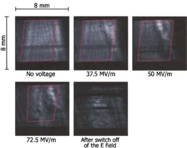
Figure 10 shows the topographical maps of the Nb sur-face, inferred from the respective interferograms in Fig. 9. At 37.5 MV/ m, the field produces a localized apex near the center, elevated by⬃20 nm above the neighboring slump. At 50 MV/ m, the surface is strongly warped and exhibits nearly a continuous crest with peak-to-valley reaching ⬃40 nm; it is noteworthy that the crest direction does not simply follow
the vertical orientation of the knife electrode. At 72.5 MV/ m, warp of the Nb layer extends further and the surface topography becomes further more complex, exhibit-ing local altitude differences of⬃50 nm.
The last interferogram in Fig. 9 was taken about 26 min after the electric field 共applied uninterruptedly over about 2 h兲 was turned off. The interferogram is not processed, be-cause of large regions without interference fringes. These black streaks are an imprint of the Nb layer partially dam-aged or stripped away from the silica substrate and suggest that a major parasitic discharge occurred during the switch off of the electrical circuit. The fringes produced by the re-maining surface are straight as in the initial interferogram, providing supplementary evidence that the surface warp ob-served throughout the sequence corresponds to actual tran-sient deformations of the Nb surface, and that these defor-mations recede after the field is switched off.
FIG. 8. Field-emission current with the Nb layer at positive potential共Nb acts as collector of electrons emitted from the knife electrode兲, accompany-ing the increasaccompany-ing bias voltage: 䊏=mean value of the current, 䉭, 〫 = minimal and maximal values detected.
FIG. 9.共Color兲 A sequence of recorded interferograms for the niobium layer at positive potential, with electric field gradually increasing from 0 共refer-ence兲 to 72.5 MV/m. The scale corresponds to the distance across the Nb surface; fringe shift by one period corresponds to surface elevation of about 100 nm. The red quadrangles correspond to regions converted to the surface maps in Fig. 10.
FIG. 10.共Color兲 Surface maps of the Nb layer at the individual values of the electric field, reconstructed from the corresponding interferograms from Fig. 9.
V. CONCLUSIONS
Soft x-ray laser interferometry at 21.2 nm was employed to visualize in situ deformations of thin niobium layers de-posited on a silica substrate, subjected to dc electric fields up to 72.5 MV m−1of both polarities. The topographical surface images obtained provide altitude resolution of ⬃2 nm, the transverse resolution across the surface is ⬃600⫻60共h
⫻v兲m2. Along the interferometric probing, field-emission current between the examined Nb surfaces and the adjacent electrode was monitored throughout the entire experiment.
The current measurements affirm that the x-ray laser does not induce field emission from the probed surface, and that the detected values of field emission and the interfero-metric data reflect authentic behavior of the Nb layers under strong electric field. Besides, the images of a layer subjected consecutively to the same values of electric fields of opposite polarity, where identical electrostatic forces are involved, in-dicate that intrinsic local characteristics of the layer are not the principal factor involved in the observed deformations.
For both polarities, the series of interferometric images reveal that the deformations of the surface are principally elastic, as these disappear after the field is switched off. This behavior of thin niobium layers differs from that of slab Nb electrodes, which were observed to retain deformations more than 1 day after the switch off of the electric field.8
The magnitude of surface deformations is much larger when the Nb layer is electron collector than when it acts as electron emitter. The presumable reason is that in the former case the layer is locally heated by the impacting electrons, emitted from the opposite knife electrode. On the other hand, the data show that topography of the Nb surface warp is rather complex, and that the change of surface relief does not simply follow the geometry of the applied field. The likely explanation is that, at high values of the applied field, the spatial distribution of the electrons emitted from the knife electrode, which subsequently impact and heat the Nb layer, does largely depend on the local features of the knife elec-trode rather than on its macroscopic profile.
The interferometric data for the Nb surface acting as electron emitter show that intermittent thermal breakdowns and current thermoflashings do not significantly modify or damage the Nb surface—within both the lateral and the alti-tude resolution, no discernible changes of the surface topog-raphy are observed after the breakdown event. On the other hand, the strong surface modifications and local damage, seen when Nb is at positive potential, suggest that sites in-ducing geometric and/or thermal field enhancement are abundantly produced on such a perturbed surface. In the case of polarity-changing rf field, these sites would contribute to a substantial increase of the amplitude of field emission.
Finally, the measurements of the field-emission current reveal that for a given value of the applied field, thermal breakdown events occur at much lower rate than for slab Nb cathodes. When the Nb layer is at the negative potential, only a few breakdown and/or current thermoflashing events is en-countered throughout the measurement sequence. At 60 MV/ m, no thermal breakdown was detected, and the field-emission current remains at a fairly low level of 0.46 nA. This suggests that thin layers are possibly of high interest for accelerator applications, and that both surface deformations and basic photoelectron emission from, e.g., Nb, Cs3Sb, or SiO2layers are worthy of further studies. ACKNOWLEDGMENTS
We gratefully acknowledge the work of the PALS laser staff, as well as the design engineering of M. Hudecek and J. C. Lagron. We further thank P. Jaeglé, K. Jungwirth, K. Rohlena, J. Ullschmied, B. Aunc, and H. Safa for their sup-port. This work financially benefited from the EU Transna-tional Access to Research Infrastructures Grant No. HPRI-00108, from the National Research Centres Project No. LN00A100 of the Ministry of Education of the Czech Re-public, and from the Czech Academy of Sciences Grant No. A1010014.
1
R. H. Fowler and L. Nordheim, Proc. R. Soc. London, Ser. A 119, 173 共1928兲.
2
D. Moffat et al., Part. Accel. 40, 85共1992兲. 3
H. Padamsee, Supercond. Sci. Technol. 14, R28共2001兲. 4
J. Knobloch, IEEE Trans. Appl. Supercond. 9, 1016共1999兲. 5
J. Graber, J. Kirchgessner, D. Moffat, J. Knobloch, H. Padamsee, and D. Rubin, Nucl. Instrum. Methods Phys. Res. A 350, 582共1994兲.
6
P. Niedermann and O. Fischer, IEEE Trans. Electr. Insul. 24, 905共1989兲. 7
J. Knobloch and H. Padamsee, Part. Accel. 53, 53共1996兲. 8
F. Albert et al., Phys. Rev. B 60, 11089共1999兲. 9
J. D. Jackson, Classical Electrodynamics, 2nd ed. 共Wiley, New York, 1975兲.
10
http: //www-cxro.lbl.gov, Center for X-ray Optics, Lawrence Berkeley Na-tional Laboratory.
11
B. Rus, T. Mocek,A. R. Präg, J. C. Lagron, M. Hudecek, G. Jamelot, and K. Rohlena, J. Phys. IV 11, Pr2-589共2001兲.
12
P. Dhez, Nucl. Instrum. Methods Phys. Res. A 261, 71共1987兲. 13
B. Rus et al., Phys. Rev. A 66, 063806共2002兲. 14
B. Rus et al., Plasma Phys. Controlled Fusion 44, B207共2002兲. 15
J. Svatos, D. Joyeux, D. Phalippou, and F. Polack, Opt. Lett. 18, 1367 共1993兲.
16
F. Polack, D. Joyeux, J. Svatos, and D. Phalippou, Rev. Sci. Instrum. 66, 2180共1995兲.
17
F. Albert et al., Opt. Commun. 142, 184共1997兲. 18
L. B. Da Silva et al., Phys. Rev. Lett. 74, 3991共1995兲. 19
J. L. A. Chilla, J. J. Rocca, O. E. Martinez, and M. C. Marconi, Opt. Lett. 21, 955共1996兲.
20
B. Rus et al., in X-Ray Lasers 2002, edited by J. J. Rocca, J. Dunn, and S. Suckewer, AIP Conf. Proc. No. 641共AIP, New York, 2002兲, p. 522. 21
J. W. Goodman, Introduction to Fourier Optics, 2nd ed.共McGraw-Hill, New York, 1996兲.
22
E. Hecht, Optics, 4th ed.共Addison-Wesley, San Francisco, 2002兲.