© 2020. ISTE OpenScience – Published by ISTE Science Publishing, London, UK – openscience.fr Page | 1
Consideration on Impacts of Electric Field and Physical
Confinement on Diffusion Constant and Carrier
Lifetime in Insulated-Gate pn-Junction Devices
Considérations sur les impacts du champ électrique et du confinement
physique sur la constante de diffusion et la durée de vie des porteurs
dans des composants à jonction pn contrôlés par grille
Yasuhisa Omura1, 2 1
Academic Collaboration Associate, Kanagawa 259-1135, Japan 2
ORDIST, KansaiI University, Suita, Osaka 564-8680, Japan
ABSTRACT. This paper discusses the impacts of electric field and physical confinement around the pn-junction on the diffusion constant and carrier lifetime of various pn-junction devices fabricated on silicon-on-insulator (SOI) substrates. The discussion will introduce the key points leading to a fuller understanding of the physics ruling the steep transfer characteristics of ‘zero subthreshold swing and zero impact ionization field-effect transistor (Z2-FET)’ fabricated on SOI substrates. First, many past experimental results of silicon-on-insulator lateral, unidirectional, bipolar-type insulated-gate transistors (SOI Lubistor) are introduced to elucidate the current-voltage characteristics of recent insulated-gate silicon-on-insulator (SOI) pn-junction devices. Advanced physics-based models are introduced to understand the physical mechanisms that should be targeted to understand the transfer characteristics of self-aligned gate SOI Luibistor, offset-gate SOI Lubistor, and Z2-FET. By combining theoretical considerations and experimental results, the physics that may determine the operating characteristics of those devices are identified from the impact of electric field and physical confinement around the pn-junction on the carrier diffusion process.
KEYWORDS. Thin SOI, semiconductor wire, pn-junction, self-aligned gate SOI Lubistor, offset-gate SOI Lubistor, Z2-FET, minority carrier lifetime, bipolar, ambipolar.
1. Introduction
The power dissipated by integrated circuits now exceeds the cooling efficiency of electronic equipment. We, therefore, have to change the design methodology of electronic devices and propose new possible semiconductor devices that dissipate far less power. This demand is strengthened by the rise of the “Internet of Things”, the attachment of sensors to literally everything that must continue to operate day and night without connection to a commercial power supply. Thus, research into a new paradigm of low-energy devices has started [CHA 10, MAR 10, CHA-L 10, DRE 10, LEE 10, VIT 10].
In order to overcome the critical technical issues, various interesting steep subthreshold swing devices, like tunnel field-effect transistors (TFETs) [BHU 04, LEO 11, MAL 13] and negative-capacitance metal-oxide-semiconductor field-effect transistors (MOSFETs) [SAL 08, LEE 15], have been extensively discussed for application to low-energy circuits and systems [OMU 16]. The ‟zero subthreshold swing and zero impact ionization field-effect transistor (Z2-FET)‟, which is one of the steep OFF-to-ON swing devices, was proposed several years ago [WAN 12, WAN 13, TAU 17, LEE 17, PAR 18, NAV 17, CRI 18] for application to low-energy circuits.
J. Wan et al. suggested in Ref. [WAN 13] that the “S-type” current-voltage characteristics of the Z2-FET is
due to the very short lifetimes of minority carriers. Although it is anticipated that the steep-switching mechanism is not so simple [TAU 17], their recent experiments addressed the very short minority carrier lifetime of the thin silicon-on-insulator (SOI) layer and investigated how the lifetime can be modeled [LEE 17,
PAR 18]. They make the simple assumption that small values of lifetime stem from the surface recombination, doping effect [SYN 14], and traps [SZE-1 07]. In contrast to their analysis, it is anticipated that other possible
© 2020. ISTE OpenScience – Published by ISTE Science Publishing, London, UK – openscience.fr Page | 2
physics must be considered because bipolar or ambipolar operation is expected from the Z2-FET [OMU 07]. Accordingly, this paper tries to elucidate the key physics that are the primary determinants of Z2-FET operation.
This paper first demonstrates some past, but important, experimental results of silicon-on-insulator lateral, unidirectional, bipolar-type insulated-gate transistors (SOI Lubistors) having the self-aligned gate structure and other pn-junction devices [OMU 07, WAK-1 03, WAK-2 03, OMU-1 13, OMU 17] in order to better understand Z2-FET carrier transport; Z2-FET operation is then briefly reviewed following the papers published [WAN 12, WAN 13, TAU 17, LEE 17, PAR 18, NAV 17, CRI 18]. After that, this paper introduces a theoretical analysis of the characteristics of the thin or wire-like SOI pn-junction diode and self-aligned-gate SOI Lubistor [OMU 82, OMU-2 13]. The theoretical consideration eliminates the confusion found in past discussions and provides a clear basis for understanding the physics of recent-proposed Z2-FET operation; that is, the very short lifetime of minority carriers stems from the electric field and the physical confinement; it is a key factor in the device physics yielding the desirable steep swing characteristic.
2. Historical Background of Silicon-on-Insulator “Insulated-Gate” pn-Junction Devices (SOI Lubistor) and Some Important Points
From the experimental results on self-aligned-gate SOI Lubistors [SZE-1 07, OMU 07] fabricated on separation by implanted oxygen (SIMOX) substrates [IZU 78] we can extract the following points.
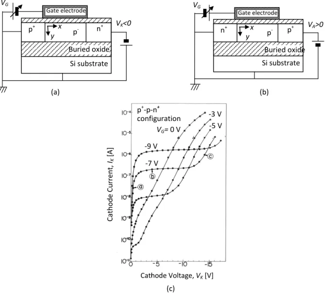
Figure 1. Schematic device structure of the self-aligned gate SOI Lubistor and IK-VK transfer characteristics.
(a) Device structure of self-aligned gate SOI Lubistor (anode grounded), (b) Device structure of self-aligned gate SOI Lubistor (cathode grounded), (c) IK-VK characteristics of self-aligned-gate SOI Lubistor given in Fig.
1(a) [OMU-3 13], where the substrate is grounded. Reproduced with permission from SOI Lubistors (Ed. Y. Omura) © 2013 John Wiley & Sons Singapore Pte.Ltd.
p+ n+ Si substrate Buried oxide p -Gate electrode VG VK<0 x y n + p+ Si substrate Buried oxide p -Gate electrode VG VA>0 x y Cathode Voltage, VK [V] Catho d e Cu rren t, IK [A] p+-p-n+ configuration LG= 50 VGm = 0 V -3 V -5 V -7 V -9 V (a) (b) (c)
© 2020. ISTE OpenScience – Published by ISTE Science Publishing, London, UK – openscience.fr Page | 3
(1) Schematic device structure of the self-aligned-gate SOI Lubistor and its typical cathode current vs. cathode voltage (IK-VK) characteristics are as shown in Fig. 1; Figures 1(a) and 1(b) show the device structures assumed in the following discussion; different bias configurations are assumed for the same structure. Figure 1(c) shows IK-VK characteristics (experimental results) obtained using a 50-m-long gate device with the SOI layer thickness of 80 nm, see Fig. 1(a) [OMU-3 13]. Self-aligned-gate SOI Lubistors show tetrode characteristics (region (b)) and triode characteristics (regions (a) and (c)). Examples of the simulation results of a 10-m-long gate device with the device structure of Fig. 1(b) are shown in Fig. 2; Figure 2(a) is obtained by assuming the standard value of carrier lifetime (~10-6 s), and Figure 2(b) is obtained by assuming a very short lifetime (~10-12 s). A comparison of experimental results and simulations suggests that the characteristics specific to self-aligned-gate SOI Lubistors with a 80-nm-thick SOI layer and a 380-nm-thick buried oxide layer shown in Fig. 2(b) are reproduced by assuming a shorter lifetime than expected [WAK-1 03, WAK-2 03].
Figure 2. Simulation results of self-aligned-gate SOI Lubistor given in Fig. 1(b) [WAK-1 03, WAK-2 03]. (a) Assumption of the standard value of carrier lifetime (~10-6 s), (b) Assumption of a very short carrier lifetime (~10-12 s). The substrate is grounded. Reproduced with permission from J. Electrochem. Soc., 150, G816
(2003). Copyright 2003, The Electrochemical Society.
(2) In Figures 1(c) and 2(b), the plateau of channel current (saturation like behavior) suggests that the drift current under the gate electrode rules the channel current due to the gate-electric-field-induced free carriers; the diffusion length of electrons is lower than expected when holes (majority carriers) are accumulated by the negative gate voltage. It has been found experimentally that the current level of the plateau is very low when the deep trap density is high near the Si/buried oxide interface. This condition yields the unique triode-like anode current vs. anode voltage (IA-VA) characteristics of the self-aligned-gate SOI Lubistor because the
electrostatic potential near the Si/buried oxide interface does not simply follow the gate potential and the anode potential [OMU 82, OMU-2 13, OMU 83], and instead the OFF state of the self-aligned-gate SOI Lubistor is triggered when negative voltage is applied to the gate electrode [OMU 82, OMU 83]. When the deep trap density is very low near the Si/buried oxide interface, the tetrode IA-VA characteristics shown in Fig. 2(b) are
observed because the electrostatic potential at the Si/buried oxide interface simply follows the gate potential and the anode potential. The IA-VA characteristics shown in Fig. 2(b) are reproduced in simulations only when a
very short lifetime is assumed [WAK-1 03, WAK-2 03], where it is not assumed that many traps exist at the Si/buried oxide interface. This is a very unique feature of the self-aligned-gate SOI Lubistor. No plateau in channel current is seen in a 5-m-long gate device fabricated with a 80-nm-thick SOI layer and a 380-nm-thick buried oxide layer shown in Fig. 2(b), while a channel current plateau was seen in a 3-m-long gate device fabricated with a 10-nm-thick SOI layer and a 80-nm-thick buried oxide layer [PET 19].
0 1 2 3 4 5 6 7 0.0 0.5 1.0 1.5 2.0 2.5 Anode voltage, VA [V] An o d e cur ren t, IA [x 1 0 -4 A] VG = 2.0V 1.5V 1.0V 0.5V 0.0V 2.5V 3.0V WG= 50 m LG= 10 m 0 1 2 3 4 5 6 7 0.0 1.0 2.0 3.0 4.0 Anode voltage, VA [V] An o d e cur ren t, IA [x 1 0 -2 A] WG= 50 m LG= 10 m VG = 0 ~ 3V Step: 0.5V (a) (b)
© 2020. ISTE OpenScience – Published by ISTE Science Publishing, London, UK – openscience.fr Page | 4
This strongly suggests that the gate-induced transverse electric field rules the diffusion length of minority carriers regardless of trap density, although the thickness of Si layer should be thin in order to physically confine carriers. Since it is expected that the diffusion constant of carriers is not decreased with the large dimensions of the device [SAT 15], we should consider that the lifetime of carriers is decreased.
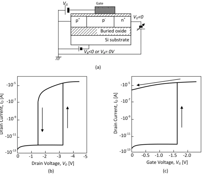
Figure 3. Schematic device structure of Z2-FET and brief review of I-V transfer characteristics. (a) Device structure of Z2-FET, (b) Brief review of ID-VD characteristics, (c) Brief review of ID-VG characteristics.
(3) On the other hand, experimental results on trap levels conducted using self-aligned-gate SOI Lubistors with 10-nm-thick SOI layer suggest that the trap levels for minority carriers are actually shallower than expected [OMU 07], and that their energy levels become shallow by increasing the gate bias [OMU-1 13, OMU 17]; it is expected that the minority carrier lifetime is increased (relatively speaking), although it is considered that this behavior of minority carrier lifetime is restricted to a very thin SOI layer (at most 10 nm). It has already been mentioned that experiments demonstrating shallower trap levels are best interpreted by the theory proposed by Hoer et al. [HOE 04]. Hoer et al. suggested that trap levels are apparently shallower than real energy levels in thin-SOI layers due to quantum-mechanical confinement and the multi-phonon process [HOE 04, HUA 50]. However, this phenomenon is not clearly observed at room temperature.
(4) The so-called „single-transistor latch‟ phenomenon has been clearly observed in thin-SOI MOSFETs [CHE 88, GAU 91]. These results suggest that „single-transistor latch‟ is, as a parasitic bipolar phenomenon, achieved even when the quality of the SOI layer is not good (the quality of SOI substrates fabricated in the 1980s and 1990s is not good due to high defect densities); the latch trigger is weak impact ionization.
(5) Recently, Ida et al. successfully demonstrated that the „PN-body-tied SOI MOSFET‟ used as an SOI
p+ n+ Si substrate Buried oxide p -Gate electrode VG VD<0 VB<0 or VB= 0V Drain Voltage, VD [V] D rai n Curr ent, ID [A] 0 -10-13 -10-11 -10-9 -10-7 -10-5 -1 -2 -3 -4 -5 Gate Voltage, VG [V] D rai n Curr ent, ID [A] 0 -10-13 -10-11 -10-9 -10-7 -10-5 -0.5 -1.0 -1.5 -2.0 (a) (b) (c)
© 2020. ISTE OpenScience – Published by ISTE Science Publishing, London, UK – openscience.fr Page | 5
MOSFET has a very steep swing [IDA 15]. The current-voltage characteristics are reproduced by assuming a standard value of minority carrier lifetime [IDA 18]; it is anticipated that the steep swing of the device substantially stems from the parasitic bipolar phenomenon; the latch trigger is not weak impact ionization.
3. Primary Aspects of Steep Output Characteristics and Steep Transfer Characteristics of Z2-FET
3.1. Steep Output Characteristics of Z2-FET
Before discussing the theoretical model introduced in this paper, the fundamental characteristics of the Z2-FET are reviewed and summarized below.
Schematic device structure of Z2-FET and schematic drain current vs. drain voltage (ID-VD) characteristics
are shown in Fig. 3 [WAN 12]; Figure 3(a) shows the device structure and Figure 3(b) shows schematic ID-VD
characteristics, where the insulated gate is aligned with the n+-type drain terminal side and the insulated-gate doesn‟t cover the p+-type source terminal side. It is assumed that the SOI layer is very thin so that the SOI layer is covered by the gate-electric-field induced free carriers. ID-VD characteristics reveal a hysteresis effect
and the hysteresis window width depends on device dimensions and carrier diffusion length. Since the gate-to-source offset structure doesn‟t allow simple double injection in the pn-junction, a relatively high drain voltage is needed for Thyristor-like switching. Simulation results described in Refs. [WAN 12, WAN 13] suggest the following points that are critical for desirable steep switching.
(1) When the electron diffusion length exceeds the gate length, the hole diffusion length must be shorter than the gate-to-source offset length for steep switching.
(2) When the hole diffusion length is longer than the gate-to-source offset length, the electron diffusion length must be shorter than the gate length for steep switching.
(3) When the electron diffusion length is longer than the gate length and the hole diffusion length is longer than the gate-to-source offset length, desirable steep switching is unavailable. Although some simulation results show weak steep switching in a very low range of current under this condition [NAV 17], it is not available for commercial applications because of its large hysteresis. It is considered that such devices would exhibit weak latch action.
(4) The potential difference around the boundary region of the Si layer beneath the gate electrode and the gate-to-source offset region can be created by the above conditions of carrier diffusion lengths ((1) and (2)). Raising the drain voltage increases the potential difference. When the potential difference reaches a critical value, Thyristor-like OFF-to-ON switching takes place.
(5) Y. Taur et al. proposed an interesting model to express the above switching behavior [TAU 17]. However, Taur et al. didn‟t address the gate-electric-field induced reduction of carrier diffusion length because the model was designed independently of carrier diffusion length. In practice, numerical values of carrier diffusion lengths assumed there don‟t satisfy the above condition of diffusion length ((1) and (2)) in the model, which suggests possibility that we must take account of the interplay of minority carrier diffusion lengths, device dimensions and doping parameters.
(6) An important point is that the carrier diffusion length is quite short for both (1) and (2), which suggests a very short carrier lifetime (~10-9 s) as is demonstrated in Refs. [WAN 12, WAN 13, TAU 17, LEE 17, PAR 18, NAV 17, CRI 18].
Recent papers discussing the physics of Z2-FET address the short carrier lifetimes [LEE 17, PAR 18]. K. H. Lee et al. suggested the influence of the doping-induced free-carrier concentration or the surface recombination
© 2020. ISTE OpenScience – Published by ISTE Science Publishing, London, UK – openscience.fr Page | 6
on the carrier lifetime [LEE 17]. Although it is well known [SZE-2 07] that high doping levels reduce carrier lifetime, this phenomenon is observed only under the charge neutral condition. The impact of the gate-electric-field-induced high-carrier-concentration condition on the carrier diffusion is discussed later again. M. S. Parihar et al. assumed the influence of traps and SOI substrate quality [PAR 18] on carrier diffusion. In those papers, the authors stressed the significant impact of short lifetime on the steep switching characteristics of the Z2-FET.
3.2. Steep Transfer Characteristics of Z2-FET
Although ID-VD characteristics were discussed in the above Section III, it is considered that drain current vs. gate voltage (ID-VG) transfer characteristics are very important from the viewpoint of conventional circuit design. Examples of ID-VG transfer characteristics are demonstrated in Ref. [WAN 12]. A schematic view of steep subthreshold behavior is shown in Fig. 3(c). The difference between Fig. 3(a) and 3(b) is the fact that the OFF state is not easily obtained, even when the gate voltage is lowered, which is due to the intrinsic Thyristor behavior. It is considered that double injection plays an important role in OFF-to-ON and ON-to-OFF switching of Z2-FET [CHE 88, GAU 91].
4. What Happens in Thin-SOI pn-Junction Devices and Insulated-Gate Thin SOI pn-Junction Devices?
4.1. Carrier Transport that should be Assumed in an Ultra-Thin SOI pn-Junction Device – Influence of Longitudinal Electric Field-
Very short diffusion lengths of carriers are currently being assumed when analyzing the ID-VD characteristics
of Z2-FETs [WAN 12, WAN 13] as was mentioned in the previous Section III. When the diffusion lengths of electrons and holes are longer than the gate length and the gate-to-source offset length, the device does not reveal large “S-like” specific steep characteristics because there is no large potential difference around the Si layer beneath the gate electrode and the gate-to-source offset region.
It has already been suggested that the self-aligned-gate thin-SOI Lubistor‟s current vs. voltage characteristics can be explained by assuming carriers with very short lifetimes [WAK-1 03, WAK-2 03], and that a similar transport property is reasonable in explaining Z2-FET transfer characteristics regardless of the crystalline quality of the SOI layer. It is expected that the carrier concentration and the channel current of self-aligned-gate SOI Lubistor and Z2-FET with a sub-100-nm-thick SOI layer is significantly modified by the self-aligned-gate electric field as is suggested in Section II. Although it is not yet clear that a single mechanism originating from minority carrier lifetimes rules the ID-VD characteristics of the Z2-FET, K. H. Lee et al. [LEE 17] and M. S. Parihar et al. [PAR 18] address the important role of very short carrier lifetimes. This strongly suggests that the lifetime of minority carriers is likely to be controlled by the transverse gate electric field [OMU-2 13, OMU 83] because the authors mention that they used a high quality SOI wafer.
When the diffusion length of minority carriers exceeds the insulated-gate length, the channel current of the self-aligned-gate SOI Lubistor cannot be well controlled as shown in Fig. 2(a) [OMU 83]; this effect is called intrinsic double injection. This characteristic is easily realized in thick SOI layers because the SOI layer is not covered by the gate-electric-field-induced free carriers [OMU 82, OMU 83], which strongly suggests that the physical confinement of the gate-electric-field-induced free carriers does play an important role both in the unique characteristics of the self-aligned-gate SOI Lubistor and in the steep switching of the Z2-FET. It can be easily expected that the transverse gate electric field enhances such carrier confinement.
Here, first, an advanced model for the gateless simplified pn-junction device [OMU-4 13] is reviewed in order to reconsider the transport of carriers in ultra-thin SOI layers and narrow wires; the influence of longitudinal electric field on the carrier transport is revisited. Following Refs. [PET 19, OMU-4 13], the
© 2020. ISTE OpenScience – Published by ISTE Science Publishing, London, UK – openscience.fr Page | 7
gradient of the quasi-Fermi level is assumed in the depletion region of pn-junction; the schematic energy band diagram is shown in Fig. 4, where the p-type region is grounded and the supply voltage of VK (< 0) is applied to
the n-type region. Although Figure 4 doesn‟t assume the conventional p+-n or n+-p configuration for simplicity, the following discussion gives an advanced viewpoint that allows better understanding of the pn-junction characteristics, and it is universal in the low-doped pn-junction.
Figure 4.Schematic energy band diagram model of the pn junction assumed in Ref. [OMU-4 13]. Reproduced with permission from SOI Lubistors (Ed. Y. Omura) ©2013 John Wiley & Sons Singapore Pte. Ltd.
The quasi-Fermi levels (imrefs) Fn(x) for electrons and Fp(x) for holes are defined inside the depletion
region using the following relations for them; that is, we assume for –Wdp<x<Wdn
( ) ( ), Fn x EFn E xn
[1] where ( ) ( ) 0, n Vk E xn [2] and ( ) ( ), Fp x EFp E xp [3] where 0E xp( ) p( Vk) [4]Here En(x) and Ep(x) give the effective variation in quasi-Fermi levels in the depletion layer (–Wdp<x<Wdn). n and p are the maximal deviations of the quasi-Fermi levels and are functions of VK. EFn and EFp give
Fermi levels of electrons and holes in the quasi-neutral regions, respectively.
The above model posits that an electric field will induce carrier drift in the depletion region. This means we must start from the following continuity equation in order to derive expressions for the carrier density and current density around the pn junction. For electron injection into the p-type region, we have
2 0 2 ( ) ( ) 0, p p p p n n p n n d n dn n n dF x D F x n dx
dx
dx [5]where Dn is the diffusion constant of electrons, np(x) is the local density of electrons, F(x) is the local electric field stemming from the gradient of quasi-Fermi level, n is the electron mobility, and n is the lifetime of
Depletion layer -Wdp 0 Wdn x qVK Fn(x) Fp(x) EFn EFp EC EV
© 2020. ISTE OpenScience – Published by ISTE Science Publishing, London, UK – openscience.fr Page | 8
electrons. The differential equation can be solved by taking the following model, where, for simplicity, we assume the doping concentration of the n-type region (ND) equals that of the p-type region (NA). A similar
discussion is possible for holes injected into the n-type region.
Here we assume that the local electric field (F(x)) primarily stems from the imref gradient because of the low doping condition. Given constant electric field F(x) for electrons in the depletion layer, we have
( ) ( ) n Dn dE x F x F qdx , [6]
where it should be noted that FDn is positive in contrast to the negative space-charge-induced field. This
electric field yields the drift current of carriers in the depletion region.
In solving Eq. [5], it is assumed that the last term is discarded because the doping level of p-type body is low, and that FDn consists only of the imref gradient. Electron current density (Jnd) in the depletion layer is given by
2 2
0 / 2
exp exp exp exp 1
( ) (0) exp exp i k n i k n n dp p n dp p dp B p B nd n n n dp n dp n qV n qV W n W p W k T p k T J qD W W
2 2 0 / 2exp exp exp 1 exp
(0) ( ) exp exp i k n i k n n dp p n dp p B p dp B n n n dp n dp n qV n qV W n W p k T p W k T qD W W 2 / 2 exp (0) i k n n Dn p B n qV q F p k T , [7]
where q is the magnitude of elementary charge, and parameters n and n are expressed as
2 2 4 2 Dn Dn B B n n qF qF k T k T L [8] 2 2 4 2 Dn Dn B B n n qF qF k T k T L , [9]
where n > 0 and n < 0. Ln is the diffusion length of electrons given by (Dnn)1/2, and it is anticipated that it
has the standard value in the quasi-neutral p-type region. n contributes to the effective diffusion length of
electrons in the p-type region. The above electron current (and hole current, not shown here) in the depletion region must be followed by the conventional diffusion current of minority carriers in the quasi-neutral p-type region given that current continuity is maintained. The current continuity is automatically maintained by the
imref gradient itself. The total junction current density (JK) is given by [OMU-4 13]
K pd nd p n
J
J
J
J
J
0 ( ) exp K p K 1 pd nd p B qV V J J J k T 0 ( ) exp K n K 1 , n B qV V J k T [10]© 2020. ISTE OpenScience – Published by ISTE Science Publishing, London, UK – openscience.fr Page | 9
In Eq. [10], Jp0 and Jn0 follow Shockley‟s definitions. The lack of the imref gradient (n=p=0) in the
depletion region means that Jnd (and Jpd in Eq. [10]) makes no contribution to the total current density, i.e., the
expression of the total current is reduced to the conventional Shockley equation.
In the quasi-neutral p-type region, the continuity equation for electrons is given by the conventional Shockley approach. The equation must be solved while taking account of the boundary condition at the edge of the depletion layer, shown in Fig. 4; according to Shockley‟s assumption, the effective potential difference at the edge of the depletion layer is given by –VK-p/q. The electron density profile in the quasi-neutral p-type
region is thus easily derived from the continuity equation.
We must assume that the nano-scale wire pn-junction has much higher local serial resistance than the conventional planar (or bulk) pn-junction; this suggests that the local gradient of the quasi-Fermi level of the wire has a finite value. It is considered that this understanding yields a better view of carrier transport even in ultra-thin SOI pn-junction devices.
Figure 5.Calculation results of 1/nLn and 1/|nLn| as a function of FDn at room temperature [OMU-4 13, PET 19]. Reproduced with permission from Advances in Engineering Research, vol. 29 (Ed. Victoria M. Petrova)
©2019 NOVA Science Publishers, Inc.
In order to visualize the behavior of n and n, for example, we show the calculation results of 1/nLn and
1/|nLn| using n and n of Eqs. [8] and [9] in Fig. 5 as a function of FDn in units of V/m because n and n
represent effective diffusion lengths. It is easily shown by using Eq. [7] that n rules the pn-junction current
when |n|>n. Thus, it is seen that 1/|nLn| is decreased as FDn is increased, and that it is very sensitive to FDn.
Since we can expect the imref gradient to be present in ultra-thin SOI layers and narrow wires, it is considered that the above theoretical prediction given by Eqs. [7], [8], and [9] will be appropriate when the carrier lifetime in the gate-to-source offset region of Z2-FET is considered.
4.2. Impacts of Insulated-Gate on Minority Carrier Diffusion in an Ultra-Thin SOI pn-Junction Device
Second, the behavior of the quasi-Fermi levels of minority carriers beneath the insulated-gate is discussed, as is the influence of the physical confinement and the transverse electric field on the carrier transport. The following assumes the schematic device structure (the self-aligned-gate SOI Lubistor [OMU 82, OMU 83]) shown in Fig. 1(a). In addition, it is assumed that the SOI layer is thin enough that the gate-electric-field-induced carriers cover the whole region of the SOI layer, and that there exist many traps at the Si/buried oxide interface. 1/|nLn | 1/(nLn) 103 102 101 1 10-1 10-2 10-3 1/( n Ln ), 1/| n Ln | 10-4 10-3 10-2 10-1 1
© 2020. ISTE OpenScience – Published by ISTE Science Publishing, London, UK – openscience.fr Page | 10
When a negative voltage is applied to the gate electrode, the energy band diagram of the device is expected to follow Fig. 6(a). It is thought that a negative gate voltage (VG <0) makes the quasi-Fermi level of holes
almost flat beneath the insulated gate because the body region is p-type. But the possible conduction path of electrons injected from the cathode is almost completely removed because the traps near the Si/buried oxide interface pin the imref of electrons at the intrinsic Fermi level; this is the “OFF state” of self-aligned-gate SOI Lubistor [OMU 83]. This “OFF” state is realized by the increase in the hole concentration induced by the gate electric field [OMU 83]. This also suggests a shorter diffusion length (shorter lifetime) of electrons under the insulated gate because the holes induced by the gate electric field significantly suppress the local electron density near the cathode [OMU 82, OMU 83].
When double injection is assumed in the insulated-gate pn-junction device, Shockley allowed the following approximate relation [SHO 49] in order to derive the simplified pn-junction current equation.
2 2 0
(
, )
0(
, )
exp
S S t t K p G p G S i BqV
p V
y dy
n V
y dy
t n
k T
, [11]where ts is the SOI layer thickness, ni denotes the intrinsic carrier concentration of the three-dimensional
intrinsic silicon, and the semi-classical condition is assumed for the SOI layer because the SOI layer thickness is not extremely thin. pp(VG,y) and np(VG,y) are the in-depth profiles of the gate-electric-field-controlled density
of holes and electrons, respectively. Equation [11] usually yields the forward-biased current of the pn junction [SHO 49].
In the self-aligned-gate SOI Lubistor, however, the “OFF” state is realized even when forward bias is applied to the n-type cathode of the self-aligned-gate SOI Lubistor [OMU 83]. Following Shockley‟s idea [SHO 49], one possible way to realize the “OFF” state is to apply the following relation to regions near the cathode and the anode of the device.
0 , 0 , s s t t p G p G p V y dy n V y dy
2 2
exp k G G s i B q V V t n k T [12]whereG is an effective body potential to suppress electron injection from the cathode and a function of the
gate voltage (VG). The negative value of G suppresses electron injection from the cathode; this idea is
supported by the experimental results of the body potential [OMU-5 13]. We will have the following relation near the cathode.
0,
s t p Gn V
y dy
. 2 2
0 exp k G G / ts , s i p G B q V V t n p V y dy k T
[13]When G is sufficiently negative, it is expected that the value of the right-hand side of Eq. [13] is very small
because the hole concentration of the body region is quite high.
On the other hand, when positive gate voltage (VG >0) is applied to the insulated gate, the quasi-Fermi level
of electrons beneath the insulated gate is not so flat because holes wait for excess electrons injected from the cathode. This significantly inclines the quasi-Fermi level of electrons under the insulated gate because the possible conductive path of electrons injected from the cathode is primarily near the top surface of the SOI layer. The quasi-Fermi level of holes is also inclined by the recombination with electrons. A possible energy band diagram is shown in Fig. 6(b); this is “ON state” of the self-aligned-gate SOI Lubistor. This phenomenon is observed when the diffusion lengths of carriers are shorter than the insulated-gate length; IK-VK
© 2020. ISTE OpenScience – Published by ISTE Science Publishing, London, UK – openscience.fr Page | 11
characteristics shown in Fig. 1(c) and IA-VA characteristics shown in Fig. 2(b) are observed. Otherwise, the simple IA-VA characteristics shown in Fig. 2(a) are observed.
It is easily anticipated that the feature of junction current depends significantly on how carrier diffusion is ruled by the local gate electric field condition in the physically confined SOI layer. In Refs. [OMU-4 13, OMU 96], it is assumed that the diffusion process of minority carriers plays an important role in the transport, and they posit the following expression for insulated-gate pn-junction devices.
Figure 6. Schematic energy band diagrams models of the insulated-gate pn junction devices. The junction configuration of the self-aligned-gate SOI Lubistor is the same as that assumed in Ref. [OMU 83, OMU-6-13] although its polarity is the counterpart of the Z2-FET shown in Ref. [WAN 13]. It is assumed for simplicity that
the substrate is grounded. (a) Negative voltage is applied to the gate of self-aligned-gate SOI Lubistor (OFF state), (b) Positive voltage is applied to the gate of self-aligned-gate SOI Lubistor (ON state), (c) OFF state of offset-gate SOI Lubistor and Z2-FET, where a negative voltage is applied to the gate electrode and a small negative voltage is applied to the n-type cathode (drain of FET), (d) ON state of self-aligned-gate and
Z2-FET, where, for example, a small negative voltage is applied to the gate electrode, but a large negative voltage is applied to the cathode (drain of Z2-FET).
0( ) exp 1 K K p n p G B qV J J J J V k T 0( ) exp 1 , K n G B qV J V k T [14] EC n-type region n+ cathode region 0 x qVK Fn(x) EFn EFp EV Fp(x) Gate electrode VG p+ anode region EC n-type region n+ cathode region 0 x qVK Fn(x) EFn EFp EV Fp(x) Gate electrode VG p+ anode region (a) (b) (c) (d) EC p-type region n+ cathode region 0 x qVK Fn(x) EFn EFp EV Fp(x) Gate electrode VG p+ anode region EC
p+ anode region n+ cathode region
0 x qVK Fn(x) EFn EFp EV Fp(x) Gate electrode VG p-type region
© 2020. ISTE OpenScience – Published by ISTE Science Publishing, London, UK – openscience.fr Page | 12
where Jp0(VG) and Jn0(VG) are empirically expressed as
0 0 ( , , ) ( ) , ( , , ) S t p n G Dp p G S P G Dp qD p V F y J V dy t L V F y
[15] 0 0 ( , , ) ( ) , ( , , ) S t n p G Dn n G S n G Dn qD n V F y J V dy t L V F y
, [16]where Lp(VG, FDp, y) and Ln(VG, FDn, y) are the in-depth profiles of the gate-electric-field-controlled diffusion
length of holes and electrons, respectively.
The electron inversion layer created by the positive gate voltage deeply covers the SOI layer because the full depletion of the SOI layer makes the potential almost flat in depth [BAL 87], and the following relation is also expected [OMU-3 13, SHO 49, OMU 96].
0
(
,
, )
0(
,
, )
S S t t p G Dp p G Dnp V F
y dy
n V F
y dy
2 2 ( ) exp K G G S i B qV V t n k T 2 2exp
K G S i BqV
q V
t n
k T
, [17]where (>0) is the dimensionless coefficient that contributes to the increase in the electron concentration in the SOI layer. It is given as
1 1 1 s BOX ox s BOX C C C C C , [18]
where Cox is the gate oxide capacitance, Cs is the SOI layer capacitance, and CBOX is the buried oxide
capacitance.
In the “ON state”, positive gate voltage increases np(VG, FDn, y) in Eq. [17]. However, those electrons
should recombine with holes coming from the anode, which suggests Ln(VG, FDn, y) is very sensitive to the gate
voltage and is forced to be shorter than the insulated-gate length if the SOI layer thickness beneath the gate electrode is very thin. Lp(VG, FDp, y) is also shorter than expected because holes are wasted by their
recombination with electrons.
When we introduce the following approximation,
0 0 0 ( , , ) ( ) , ( , , ) S S t p n G Dp p G t P G Dp qD p V F y dy J V L V F y dy
[19] 0 0 0 ( , , ) ( ) , ( , , ) S S t n p G Dn n G t n G Dn qD n V F y dy J V L V F y dy
[20]© 2020. ISTE OpenScience – Published by ISTE Science Publishing, London, UK – openscience.fr Page | 13
Eq. [14] can be rewritten as
2 2 2 2 0 ( , , ) 0 ( , , ) 0 ( , , ) 0 ( , , ) S S S S p S i n S i K t t t t P G Dp n G Dn n G Dn p G Dp qD t n qD t n J L V F y dy n V F y dy L V F y dy p V F y dy
2 exp K G , B qV q V k T [21]where Eq. [17] is used. This equation can be simplified to
2 2 0 ( , , ) 0 ( , , ) S S p S i n S i K t t D P G Dp A n G Dn qD t n qD t n J N L V F y dy N L V F y dy
2 exp K G , B qV q V k T [22]where ND and NA are the averaged doping concentration of donors and acceptors, respectively. The validity of
Eq. [22] can be easily examined using current vs. voltage characteristics of region © shown in Fig. 1(c) and in Fig. 2(b). In addition, Equation [22] reveals the following:
(1) When values of Lp(VG, FDp, y) and Ln(VG, FDn, y) are very small, JK takes a very large value. This yields
the visible plateau in Fig. 1(c), although the leakage current of reverse-biased devices should be increased. This is the case of carriers with short lifetime.
(2) When values of Lp(VG, FDp, y) and Ln(VG, FDn, y) are very large, JK takes a very small value. This means
the annihilation of visible plateau in Fig. 1(c), although the leakage current of reverse-biased device should be reduced. This is the case of carriers with long lifetime.
The above suggestions given by Eq. [22] are very meaningful in the following discussion.
4.3. Offset-gate SOI Lubistor and Z2-FET
This paper now addresses the Z2-FET transfer characteristics. Figure 6(c) shows the schematic energy band diagram of the “OFF” state Z2-FET and Figure 6(d) that of the “ON” state (not transient state) Z2-FET, where the p++-n-n++ configuration is assumed to allow comparison with the offset-gate SOI Lubistor [OMU 83, OMU-6 13]. It is also assumed for simplicity that the substrate is grounded. IK vs. VK current characteristics of the offset-gate SOI Lubistor are shown in Fig. 7 [OMU 83]. The offset-gate SOI Lubistor reveals bipolar action similar to the Z2-FET, although its S-like switching voltage is higher than that of the Z2-FET because the gate length is very long (5 m) [OMU 83, OMU-6 13].
In the “OFF state” Z2-FET and the offset-gate SOI Lubistor shown in Fig. 6(c), a negative voltage is applied to the gate electrode and a negative, but small, voltage is applied to the n-type drain. A hole inversion layer is created beneath the gate electrode; the injection of electrons from the drain is suppressed because the electron diffusion length is shorter than the gate length so the drain bias is too low to induce electron injection from the drain. Even when the negative voltage to the gate electrode rises up to the energy barrier between the gate-to-source offset region and the body region beneath the gate electrode, desirable OFF-to-ON steep switching does not easily take place if the specific requirements of the electron diffusion length and the hole diffusion length mentioned in Section III-A are not satisfied.
Desirable OFF-to-ON steep switching takes place when the drain bias takes a certain value higher than the potential difference between the gate-to-source offset region and the body region beneath the gate electrode and the specific requirements of carrier diffusion lengths described above are satisfied.
© 2020. ISTE OpenScience – Published by ISTE Science Publishing, London, UK – openscience.fr Page | 14 Ambipolar leakage current due to electrons and holes between the gate-to-source offset region and the body region beneath the gate electrode break the potential barrier. The possible schematic energy band diagram in the “ON state” after the transient process is shown in Fig. 6(d), where quasi-Fermi levels of electrons and holes are split off. The carrier flow beneath the gate electrode is expected to form the ambipolar current due to the gate electric field although it is intrinsically the bipolar current in the gate-to-source offset region. Thus, it is anticipated that these “OFF state” conditions and the OFF-to-ON switching behavior of Z2-FET are roughly the same as the bipolar action of the offset-gate SOI Lubistor, see Fig. 7.
Figure 7. IK-VK transfer characteristics of the offset-gate SOI Lubistor [OMU 83]. The gate length is 5 m. The
buried oxide is 470 nm thick. The parasitic bipolar action is seen at the cathode voltage of about -20 V and at the gate voltage of 0 V. Reproduced with permission from SOI Lubistors (Ed. Y. Omura) ©2013 John Wiley &
Sons Singapore Pte. Ltd. (a) Whole view of IK-VK characteristics, (b) A local view of IK-VK characteristics.
In the “OFF state” Z2-FET and the offset-gate SOI Lubistor shown in Fig. 6(c), a negative voltage is applied to the gate electrode and a negative, but small, voltage is applied to the n-type drain. A hole inversion layer is created beneath the gate electrode; the injection of electrons from the drain is suppressed because the electron diffusion length is shorter than the gate length so the drain bias is too low to induce electron injection from the drain. Even when the negative voltage to the gate electrode rises up to the energy barrier between the gate-to-source offset region and the body region beneath the gate electrode, desirable OFF-to-ON steep switching does not easily take place if the specific requirements of the electron diffusion length and the hole diffusion length mentioned in Section III-A are not satisfied.
Desirable OFF-to-ON steep switching takes place when the drain bias takes a certain value higher than the potential difference between the gate-to-source offset region and the body region beneath the gate electrode and the specific requirements of carrier diffusion lengths described above are satisfied. Ambipolar leakage current due to electrons and holes between the gate-to-source offset region and the body region beneath the gate electrode break the potential barrier. The possible schematic energy band diagram in the “ON state” after the transient process is shown in Fig. 6(d), where quasi-Fermi levels of electrons and holes are split off. The carrier flow beneath the gate electrode is expected to form the ambipolar current due to the gate electric field although it is intrinsically the bipolar current in the gate-to-source offset region. Thus, it is anticipated that these “OFF
IK VK Snap-back VG= 0V Breakdown (a) (b)
© 2020. ISTE OpenScience – Published by ISTE Science Publishing, London, UK – openscience.fr Page | 15
state” conditions and the OFF-to-ON switching behavior of Z2-FET are roughly the same as the bipolar action of the offset-gate SOI Lubistor, see Fig. 7.
Finally, some points are addressed. We can assume that nano-scale pn-junction devices have larger local body resistance than bulk pn-junction devices, and thus that they exhibit a gradient in the local quasi-Fermi level in the forward-bias pn-junction. Nano-scale pn-junction devices with the gate-all-around MOS structure surrounding the body region are expected to exhibit a transport phenomenon similar to the above because the insulated-gate-induced electric field forcibly shortens the minority-carrier diffusion length. This satisfies the physical condition of steep switching of Z2-FET that has been mentioned in Section III. Thus, it is considered that the insulated-gate-electric-field-induced reduction and the longitudinal-electric-field-induced reduction of minority-carrier diffusion length are the primary physics triggering the steep transfer characteristics of the “Z2-FET”.
5. Conclusion
This paper briefly reviewed the physics and conditions determining the unique characteristics of SOI Lubistor and Z2-FET, and introduced advanced physics that should be considered in designing such specific thin SOI pn-junction devices. Based on theoretical considerations, this paper has suggested that the lifetime of minority carriers of Si nano-scale wire pn-junction devices and ultra-thin silicon-on-insulator pn-junction devices is reduced by the longitudinal and transversal electric fields even when the material quality is quite high. While this unique behavior of minority carrier diffusion has not been discussed comprehensively so far, this paper suggests that the theoretical model described here gives a possible appropriate understanding of device characteristics; that is, the reductions in the carrier lifetime due to the longitudinal electric field and/or the insulated-gate-induced transverse electric field yield the desirable steep switching behavior of Z2-FET. In addition, this paper demonstrated that the output characteristics of Z2-FET are very similar to those of the offset-gate SOI Lubistor, where it is anticipated that the gate length and the gate-offset-region length are much longer than carrier diffusion lengths of electrons and holes. Thus, the steep switching behavior of Z2-FET can be explained by assuming the above carrier transport aspects. The discussion in this paper will remain valid even in future nano-scale pn-junction structures.
References
[CHA 10] Chandrakasan, A. P., Daly, D. C., Finchelstein, D. F., Kwong, J., Rmadass, Y. K., Sinangil, M. E., Sze, V., and Verma, N., Technologies for Ultradynamic Voltage Scaling, Proc. IEEE, 98, p. 191-214, 2010.
[MAR 10] Markovic, D., Wang, C. C., Alarcon, L. P., Liu, T.-T., and Rabaey, J. M., Ultralow-Power Design in Near-Threshold Region, Proc. IEEE, 98, p. 237-252, 2010.
[CHA-L 10] Chang, L., Frank, D. J., Montoye, R. K., Koester, S. J., Ji, B. L., Coteus, P. W., Dennard, R. H., and Haensch, W., Practical Strategies for Power-Efficient Computing Technologies, Proc. IEEE, 98, p. 215-236, 2010.
[DRE 10] Dreslinski, R. G., Wieckowski, M., Blaauw, D., Sylvester, D., and Mudge, T., Near-Threshold Computing: Reclaiming Moore‟s Law Through Energy Efficient Integrated Circuits, Proc. IEEE, 98, p. 253-266, 2010.
[LEE 10] Lee, H.-S., Brooks, L., and Sodini, C. G., Zero-Crossing-Based Ultra-Low-Power A/D Converters, Proc. IEEE, 98, p. 315-332, 2010.
[VIT 10] Vitale, S. A., Wyatt, P. W., Checka, N., Kedzierski, J., and Keast, C. L., FDSOI Process Technology for Subthreshold-Operation Ultralow-Power Electronics, Proc. IEEE, 98, p. 333-342, 2010.
[BHU 04] Bhuwalka, K. K., Sedlmaier, S., Ludsteck, A. K., Tolksdorf, C., Schulze, J., and Eisele, I., Vertical tunnel field-effect transistor, IEEE Trans. Electron Devices, 51, p. 279-282, 2004.
[LEO 11] Leonelli, D., Vandooren, A., Rooyachers, R., Verhulst, A. S., Huyghebaert, C., Gendt, S. D., Heyns, M. M., and Groeseneken, G., Novel Architecture to Boost the Vertical Tunneling in Tunnel Field Effect Transistors, Proc. IEEE Int.
SOI Conf. p. 1-2, 2011.
© 2020. ISTE OpenScience – Published by ISTE Science Publishing, London, UK – openscience.fr Page | 16 Characteristics of a Silicon Tunnel Field-Effect Transistor Based on Vertical Tunneling, IEEE Trans. Electron Devices, 60, p. 935-843, 2013.
[SAL 08] Salahuddin, S. and Datta, S., Use of Negative Capacitance to Provide Voltage Amplification for Low Power Nanoscale Devices, Nanoletters, 8, p. 405-410, 2008.
[LEE 15] Lee, M. H., Chen, P. G., Liu, C., Chu, K. Y., Cheng, C. C., Xie, M. J., Liu, S. N., Lee, J. W., Huang, S. J., Liao, M. H., Tang, M., Li, K. S., and Chen, M. C., Prospects for ferroelectric HfZrOx FETs with experimentally CET=0.98nm, SSfor=42mV/dec, SSrev=28mV/dec, switch-off <0.2V, and hysteresis-free strategies, Tech. Dig. IEEE IEDM (San Francisco, 2015), paper ID 22.5.
[OMU 16] Omura, Y., Mallik, A., and Matsuo, N., MOS Devices for Low-Energy and Low-Voltage Applications, IEEE Press/Wiley, 2016.
[WAN 12] Wan, J., Le Royer, C., Zaslavsky, A., and Cristoloveanu, S., Z2-FET: A zero-slope switching device with gate-controlled hysteresis, Tech. Dig. Int. VLSI Tech. Sys. And Appl., (Hsinchu, 2012); DOI: 10.1109/VLSI-TSA.2012.6210113.
[WAN 13] Wan, J., Royer, C. L., Zaslavsky, A., and Cristoloveanu, S., A systematic study of the sharp-switching Z2-FET device: From mechanism to modeling and compact memory applications, Solid-St. Electron., 90, p. 2-11, 2013.
[TAU 17] Taur, Y., Lacord, J., Parihar, M. S., Wand, J., Martinie, S., Lee, K., Bawedin, M., Barbe, J.-C., Cristoloveanu, S., A comprehensive model on field-effect pnpn devices (Z2-FET), Solid-St. Electron., 134, p. 1-8, 2017.
[LEE 17] Lee, K. H., Bawedin, M., Park, H.-J., Parihar, M., and Cristoloveanu, S., Carrier Lifetime Evaluation in FD-SOI Layers, Proc. ESSDERC (Leuven, Sep., 2017), p. 140-143.
[PAR 18] Parihar, M. S., Lee, K. H., Park, H. J., Lacord, J., Martinie, S., Barbe, J.-C., Xu, Y., Dirani, H. E., Taur, Y., and Cristoloveanu, S., Insight into Carrier Lifetime Impact on Band-modulation Devices, Solid State Electron., 143, p. 41-48, 2018.
[NAV 17] Navarro, C., Lacord, J., Parihar, M. S., Adamu-Lema, F., Duan, M., Rodriguez, N., Cheng, B., Dirani, H. E., Barbe, J.-C., Fonteneau, P., Bawedin, M., Millar, C., Galy, P., Royer, C. L., Karg, S., Wells, P., Kim, Y.-T., Asenov, A., Cristoloveanu, S., and Gamitz, F., Extended Analysis of the Z2-FET: Operation as Capacitorless eDRAM, IEEE Trans.
Electron Devices, 64, p. 4486-4491, 2017.
[CRI 18] Cristoloveanu, S., Lee, K. H., Parihar, M. S., Dirani, H. E., Lacord, J., Martinie, S., Royer, C. L., Barbe, J.-C., Mescot, X., Fonteneau, P., Galy, P., Gamitz, F., Navarro, C., Cheng, B., Duan, M., Adamu-Lema, F., Asenov, A., Taur, Y., Yu, X., Kim, Y.-T., Wan, J., and Bawedin, M., A Review of the Z2-FET 1TDRAM Memory: Operation Mechanisms and Key Parameters, Solid State Electron., 143, p. 10-19, 2018.
[SYN 14] Synopsys Sentaurus TCAD, Operations Manual, ver. J-2014.09.
[SZE-1 07] Sze, S. M. and Ng, K. K., Physics of Semiconductor Devices, 3rd Ed. Wiley, New York, 2007, p. 43-44. [OMU 07] Omura, Y., Experimental study of two-dimensional confinement effects on reverse-biased current
characteristics of ultrathin silicon-on-insulator lateral, unidirectional, bipolar-type insulated-gate transistors, Jpn. J.
Appl. Phys., 46, p. 2968-2972, 2007.
[WAK-1 03] Wakita, S. and Omura, Y., Sub-circuit models of silicon-on-insulator insulated-gate pn-junction devices for electrostatic discharge protection circuit design and their applications, Solid-State Electron., 47, p. 1943-1952, 2003. [WAK-2 03] Wakita, S. and Omura, Y., Device Models of Silicon-on-Insulator Insulated-Gate pn-Junction Devices, J. the
Electrochem. Soc., 150, p. G816-G820, 2003.
[OMU-1 13] Omura, Y., SOI Lubistors, IEEE Press/Wiley, 2013, Chapter 13, p. 157.
[OMU 17] Omura, Y., Mori, Y., Sato, S., and Mallik, A., Revisiting the Role of Trap-Assisted-Tunneling Process on Current-Voltage Characteristics in Tunnel Field-Effect Transistors, J. Appl. Phys., 123, p. 161549-1-161549-6, 2017. [OMU 82] Omura, Y., Lateral, Unidirectional, Bipolar-type, Insulated-gate Transistors – A nobel semicon doctor device,
Appl. Phys. Lett., 40, p. 528-529, 1982.
[OMU-2 13] Omura, Y., SOI Lubistors, IEEE Press/Wiley, 2013, Part II.
[IZU 78] Izumi, K., Doken, M., and Ariyoshi, H., CMOS Devices Fabricated on Buried SiO2 Layers Formed by Oxygen Implantation into Silicon, Electron. Lett., 14, p. 593-594, 1978.
[OMU-3 13] Omura, Y., SOI Lubistors, IEEE Press/Wiley, 2013, Chapter 5.
© 2020. ISTE OpenScience – Published by ISTE Science Publishing, London, UK – openscience.fr Page | 17 263-266, 1983.
[PET 19] Petrova, V. M., Advances in Engineering Research, vol. 29, NOVA Science Publishers, Inc. 2019, Figure 6 in Chapter 5.
[SAT 15] Sato, S. and Omura, Y., Possible Theoretical Models for Carrier Diffusion Coefficient of One-Dimensional Si Wire Devices, Jpn. J. Appl. Phys., 54, p. 054001-1-054001-7, 2015.
[HOE 04] Hoer, T., Schenk, A., and Fichtner, W., Revised Shockley-Read-Hall lifetimes for quantum transport modeling,
J. Appl. Phys., 95, p. 4875-4882, 2004.
[HUA 50] Huang, K. and Rhys, A., Theory of light absorption and non-radiative transition in F-centers, Proc. The Royal
Soc. London, A204, p. 406-423, 1950.
[CHE 88] Chen, C.-D., Matloubian, M., Sundaresan, R., Mao, B.-Y., Wei, C.-C., and Pollack, G. P., Single-transistor latch in SOI MOSFETs, IEEE Electron Device Lett., 9, p. 636-638, 1988.
[GAU 91] Gautier, J. and Auberton-Herve, A.-J., A latch phenomenon in buried N-body SOI NMOSFET's, IEEE Electron
Device Lett., 12, p. 372-374, 1991.
[IDA 15] Ida, J., Mori, T., Kuramoto, Y., Horii, T., Yoshida, T., Takeda, K., Kasai, H., Okihara, M., and Arai, Y., Super Steep Subthreshold Slope PN-Body Tied SOI FET with Ultra Low Drain Voltage down to 0.1V, Tech. Dig. IEEE
IEDM (San Francisco, 2015), p. 624-627.
[IDA 18] Private communication with Prof. J. Ida (Kanazawa Institute of Technology), 2018.
[SZE-2 07] Sze, S. M. and Ng, K. K., Physics of Semiconductor Devices, Wiley, New York, 2007, p. 40-43. [OMU-4 13] Omura, Y., SOI Lubistors, IEEE Press/Wiley, Singapore, 2013, Chapter 2.
[SHO 49] Shockley, W., The Theory of p-n Junction in Semiconductors and p-n Junction Transistors, The Bell Sys. Tech.
J., 28, p. 435-489, 1949.
[OMU-5 13] Omura, Y., SOI Lubistors, IEEE Press/Wiley, Singapore, 2013, Fig. 5.9 in page 56.
[OMU 96] Omura, Y., Two-Dimensionally Confined Injection Phenomena at Low Temperatures in Sub-10-nm-Thick SOI Insulated-Gate p-n-Junction Devices, IEEE Trans. on Electron Devices, 43, p. 436-443, 1996.
[BAL 87] Balestra, F., Cristoloveanu, S., Benachir, M., Brini, J., and Elewa, T., Double-Gate Silicon-on-Insulator with Volume Inversion: a new Device with greatly Enhanced Performance, IEEE Electron Devices Lett., EDL-8, p. 410-412, 1987.
![Figure 2. Simulation results of self-aligned-gate SOI Lubistor given in Fig. 1(b) [ WAK-1 03, WAK-2 03 ]](https://thumb-eu.123doks.com/thumbv2/123doknet/15034229.689359/3.892.97.754.318.623/figure-simulation-results-self-aligned-gate-lubistor-given.webp)
![Figure 4. Schematic energy band diagram model of the pn junction assumed in Ref. [OMU-4 13]](https://thumb-eu.123doks.com/thumbv2/123doknet/15034229.689359/7.892.236.627.155.420/figure-schematic-energy-band-diagram-model-junction-assumed.webp)
![Figure 5. Calculation results of 1/ n L n and 1/| n L n | as a function of F Dn at room temperature [ OMU-4 13, PET 19 ]](https://thumb-eu.123doks.com/thumbv2/123doknet/15034229.689359/9.892.254.589.354.670/figure-calculation-results-function-room-temperature-omu-pet.webp)

![Figure 7. I K -V K transfer characteristics of the offset-gate SOI Lubistor [OMU 83]](https://thumb-eu.123doks.com/thumbv2/123doknet/15034229.689359/14.892.85.772.230.595/figure-transfer-characteristics-offset-gate-soi-lubistor-omu.webp)
