Characterization of Commercial Step-Down
Converter Performance in the Low Earth Orbit
Radiation Environment
by
Alexa Christine Aguilar
Submitted to the Department of Aeronautics and Astronautics
in partial fulfillment of the requirements for the degree of
Master of Science in Aeronautics and Astronautics
at the
MASSACHUSETTS INSTITUTE OF TECHNOLOGY
June 2019
@
Massachusetts Institute of Technology 2019. All rights reserved.
Signature redacted
A uthor ...
...
Departrmnent of Aeronautics and Astronautics
May 22, 2019
Certified by ...
Signature redacted
Kerri Cahoy
Associate Professor of Aeronautics and Astronautics
Thesis Supervisor
Signature redacted
A ccepted by ...
...
MASSACHUSETTS INSTITUTE OF TECHNOLOGYJUL
0 12019
LIBRARIES
Sertac Karaman
Associate Professor of Aeronautics and Astronautics
Chair, Graduate Program Committee
Characterization of Commercial Step-Down Converter
Performance in the Low Earth Orbit Radiation Environment
by
Alexa Christine Aguilar
Submitted to the Department of Aeronautics and Astronautics on May 22, 2019, in partial fulfillment of the
requirements for the degree of
Master of Science in Aeronautics and Astronautics
Abstract
We characterize three commercial step-down DC-DC converters for the Low Earth Orbit (LEO) space radiation environment. Commercial space industry is shifting spacecraft design philosophy toward accepting more risk for shorter lead times, lower costs, and high instrument performance. This shift opens up the Commercial Off The Shelf (COTS) electronics market to space applications. To quantify the risks associ-ated with using COTS parts, components must be tested in flight-like configurations and conditions and their response to environmental stresses characterized. Few data exist in literature on the performance of DC-DC converters in the space radiation environment despite their ubiquity in designs and key role in operation for which the alternative is prohibitively expensive.
This thesis introduces the space radiation environment and resulting effects. We then model the environment for two LEO constellation configurations and determine the maximum expected radiation levels over the mission lifetime. These levels are then used to inform radiation tests.
The DC-DC converters are Total Ionizing Dose (TID) and Single Event Effects
(SEE) tested in radiation conditions representative of the LEO space radiation
envi-ronment. These devices demonstrate radiation tolerance in both tests, with a mini-mum TID tolerance of 60 krad(Si) and experience no destructive latch-up behavior to about 90 MeV-cm2-mg-1. A first order reliability analysis shows these parts introduce little additive risk to spacecraft design.
Thesis Supervisor: Kerri Cahoy
Acknowledgments
I would first like to thank my advisor Dr. Kerri Cahoy for her guidance and unfailing
support during my time at MIT. Her drive and technical prowess are unparalleled and I would not be where I am in my academic and professional career without her.
I would also like to thank Dr. Randall Milanowski for his technical guidance
and expertise on radiation. I truly appreciate all the instruction he has offered in using OMERE, designing tests, and interpreting results. Additional thanks to Steve McClure for his knowledge of radiation effects on electronics. Both of their support of this project was instrumental in its success and timeliness.
I would also like to acknowledge Dr. Slaven Moro and Raichelle Aniceto for giving
me the opportunity to work on this project. I sincerely appreciate the chance to work in the radiation effects field.
Finally, I would like to thank my parents, Buster and Francie Aguilar, for their unwavering support and encouragement during my time in MIT's Department of Aeronautics and Astronautics.
Contents
1 Introduction 17
1.1 Motivation for Optical Communications . . . . 19
1.1.1 Existing Optical Communication Systems . . . . 20
1.2 Motivation for Commercial Off the Shelf Components . . . . 22
1.2.1 Motivation for Commercial DC-DC Converters . . . . 25
1.3 Overview of this work . . . . 26
2 The Earth Radiation Environment 29 2.1 Low Earth Orbit Radiation Environment . . . . 29
2.1.1 Solar Radiation . . . . 29
2.1.2 Trapped Particles . . . . 30
2.1.3 Galactic Cosmic Rays . . . . 31
2.2 Radiation Effects on Electronics in LEO . . . . 33
2.2.1 Total Ionizing Dose . . . . 34
2.2.2 Displacement Damage . . . . 36
2.2.3 Single Event Effects . . . . 38
2.2.4 Upset Rate Calculations . . . . 41
2.2.5 Reliability Analysis . . . . . ... . . . . 44
2.3 OMERE Analyses for LEO Missions . . . . 45
3 TID and SEE Experiments 53 3.1 Total Ionizing Dose (TID) Testing . . . . 54
3.1.2 3.1.3 3.2 Single 3.2.1 3.2.2 3.2.3 3.2.4 Board Configuration .
TID Levels and Test Setup.
Event Effects (SEE) Testing
Test Parameters . . . . Board Configuration . Ion Selection . . . . Test Setup . . . . 4 Results 4.1 TID Results . . . . 4.2 SEE Test Results . . . . 4.2.1 Upset Rates . . . . 4.2.2 Failure Analysis . . . .
5 Conclusion and Future Work
5.1 Conclusion . . . .
5.2 Future Work . . . . A Weibull Curve Estimation Code
55 57 58 58 59 59 62 65 65 69 74 77 79 79 80 83
List of Figures
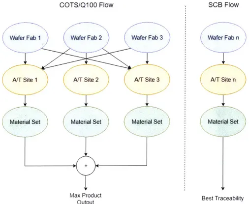
1-1 Each wafer fabrication facility, assembly and test (A/T) facility, and material set facility change operations and process to optimize for max-imum yield locally. Singe Controlled Baseline (SCB) reduces manufac-turing variability [7]. . . . . 23
1-2 Component Grade Spectrum from Texas Instruments
[6].
Commer-cial, Automotive(Q100),
Enhanced Performance (EP), and Qualified Manufacturers List (QML) components span the range of available parts. 241-3 Typical buck converter topology . . . . 25
2-1 Integral flux of Trapped Electrons generated using OMERE 5.2.2 using the AE8 model for trapped electrons with the Jensen Cain Model, according to ECSS-10 Standards. . . . . 30
2-2 Integral flux of Trapped Protons generated using OMERE 5.2.2 using the AP8 model for trapped electrons with the Jensen Cain Model, according to ECSS-10 Standards. . . . . 31
2-3 Increased proton flux known as the South Atlantic Anomaly at lower latitudes due to the offset in Earth's magnetic field axis and rotation ax is. . . . . 3 2
2-4 Cross-section and corresponding device representation of a Metal Oxide Semiconductor Field Effect Transistor (MOSFET). The device activi-tates and allows current to flow between the Drain (D) and Source (S) when the Gate (G) voltage exceeds the voltage between D and S. . . 33
2-5 MOSFET Operation under nominal conditions (a) and post-irradiation (b). Charge accumulates in the gate oxide over time and reduces the
amount of voltage required to turn the device on. Eventually, if the cumulative dose is high enough, a permanent conduction channel will form, and the device cannot be turned off even if 0 V is applied at the gate [49]. . . . . 35 2-6 Bragg Curve for Neon in Silicon. Initial Energy for Neon is 1 GeV.
Bragg peak occurs at 350 mm [8]. . . . . 39 2-7 Cross section of CMOS transistor showing parasitic BJTs. Each NPN
and PNP junction creates a parasitic BJT within a CMOS device. When current flows through these regions, a regenerative gain state is activated, creating a run-away current state. Resistances are from the bulk and substrate materials [8]. . . . . 41
2-8 Summary of energetic particles and radiation effect contributions. . . 42
2-9 Notional Cross Section Curve for a device with target material of Sil-icon. Note the cross section curve is sensitive to ion incident angle
[8]. . . . . 4 3 2-10 Bathtub curve illustrating the lifetime sections of a given component
[4 4]. . . . . 4 5
2-11 Each constellation has a 10-year operational lifetime with 2 years of in-orbit storage. The simulation start date is set for January 1, 2022
[18]. . . . . 4 7
2-12 Total Ionizing Dose as a function of shielding thickness. Values at 100 mils (2.54 mm), 200mils (5.08 mm), and 300 mils (7.62 mm) are marked. 48
2-13 Displacement Damage Dose Analysis from OMERE 5.2.2.
Displace-ment damage dose is analogous to total dose depth and captures the amount of non-ionizing damage in Silicon for a given shielding thick-ness. Equivalent fluence is useful for testing purposes and may be used to determine the total number of mono-energetic particles needed to induce the same level non-ionizing damage. . . . . 50
2-14 Integral flux spectrum for reference cases in the LEO radiation envi-ronm ent... . ... ...51
3-1 Simplified layout of the load board used to induce Full Load (high
current) conditions. The 555-timer is set to a 2.86% (400s/14ms) duty cycle. The output is inverted and applied to the gate of a NFET, which would momentarily connect the resistor network to ground, drawing higher currents from the DUTs. This mode is used to observe transient responses as a function of dose. The switch can be enabled manually, and is used to observe total high current draw and calculate conversion efficiency as a function of dose. . . . . 56
3-2 TID Test Setup. The converters are exposed to gamma radiation in the Cobalt-60 source while other sensitive electronics, such as the load boards, power supplies, and monitoring hardware, are located outside the irradiation chamber. . . . . 57
3-3 Ions and Energies for Electronics Testing Provided by NSRL [12]. . . 59 3-4 Calculated Xenon Bragg curve for target material of Silicon and initial
energy. . . . . . . . 61
3-5 Calculated Tantalum Bragg curve for target material of Silicon and initial energy. . . . . 61
3-6 Calculated Gold Bragg curve for target material of Silicon and initial
energy. . . . ...62
3-7 Block diagram of the SEE test setup. The DUT input voltage and
current, output voltage and current, and temperature are monitored rem otely during testing. . . . . 63
3-8 Evaluation board on the NSRL beam line during SEE testing . . . . 64
4-1 Output Voltage vs Dose. The 4A device exhibits highest sensitivity to radiation, showing the largest output shift (19 mV in set 1). . . . . . 66
4-2 Input Current vs. Dose for No Load Testing. The 8A and 12A part show highest sensitivity, and input current increase is seen between 50 and 60 krad(Si). . . . . 67
4-3 Input Current vs. Dose for Light Load Testing. The 8A and 12A part show highest sensitivity, and input current increase is seen between 50 and 60 krad(Si) . . . . 67
4-4 Input Current vs Dose for Full Load Testing. None of the devices exhibited sensitivity in this test mode . . . . 68
4-5 Efficiency vs Dose for Light Load Testing. Decreases in efficiency pre-cede failure thresholds. The 4A device begins decreasing in efficiency around 50 krad(Si). The 8A and 12A devices begin decreasing around
60 and 70 krad(Si). . . . . 68
4-6 Efficiency vs Dose for Full Load Testing. The 4A and 8A devices exhibit increases in efficiency. This is potentially caused by control circuit intervention and internal regulation. . . . . 69
4-7 Transient Response of 8A device at 40 krad(Si). . . . . 69
4-8 Transient Response of 8A device at 70 krad(Si). Output is similar to 40 krad(Si) output. . . . . 70
4-9 Transient Response of 8A device at 80 krad(Si). Output is reduced compared to 40 and 70 krad(Si) response. . . . . 70
4-10 4A Cross Section with S = 1 and W = 20. The onset LET is 14 MeV-cm2-mg-1 and saturates at 3E-5 cm2 . . . . . . . . 71
4-11 Transient events observed on the 4A Device. a-c shos oscillations on Vou, and D shows transients on POK. . . . . 72
4-12 8A Cross Section with S = 1 and W = 19. The onset LET is 14
4-13 SEE events observed in th 8A device. a is persistent shutdown where POK and V0st fall to 0 V and require an external power cycle to return to nominal operations. b is a shutdown with attempt at restart that requires an external power cycle. c is a transient shutdown where the device autonomously returned to nominal operation. d is a V0"t transient with little change to overall output level. . . . . 74 4-14 12A Cross Section with S 1 and W = 24. The onset LET is 14
MeV-cm2-mg1 and saturates at 2.2E-6 cm2. . . . 75
4-15 SEE Events in 12A Device. a is a persistent shutdown that requires ex-ternal power cycling. b is a shutdown with restart event that requires external power cycling. c is a transient shutdown event. d is a V,"t transient. Note that the oscilloscope was triggered to record an event, but the sampling rate was insufficient to capture the microsecond du-ration. Had an event been observed, it would have looked similar to c but with smaller amplitude change in POK. . . . . 76
List of Tables
1.1 Demonstrated Optical Communication Systems . . . . 21
1.2 Comparison of 28V Input Hybrid DC-DC Converters . . . . 26
2.1 Displacement damage energy thresholds for common materials suscep-tible to TNID [49]. Optoelectronics such as photodetectors (PD) will often use these materials. . . . . 37
2.2 Single Event Effects Relevant to Hybrid DC-DC Converters . . . . . 40
2.3 Summary of LEO Constellation Mission from Telesat FCC Filing [18] 46 2.4 Radiation Analyses Summary for Telesat Constellations . . . . 49
3.1 Nominal operating conditions and parameters for tested DC-DC con-verters . . . . 53
3.2 TID Test Electrical Configuration. All devices are tested under bias. A total of 3 loading conditions are tested to determine parameter shifts as a function of total dose. . . . . 55
3.3 SEE Test Conditions . . . . 62
4.1 4A Telesat Inclined Upset Rates . . . . 76
4.2 4A Telesat Polar Upset Rates . . . . 76
4.3 8A Telesat Inclined Upset Rates . . . . 77
4.4 8A Telesat Polar Upset Rates . . . . 77
4.5 12A Telesat Inclined Upset Rates . . . . 77
Chapter 1
Introduction
Predictions by Morgan Stanley estimate the global satellite industry could generate
$1.1 billion in revenue by 2040, half of which is attributed to growth of broadband
internet [43]. This growth is being driven by exponentially-increasing data demands in applications such as mobile internet, autonomous vehicles, and Internet of Things
(IoT)
[43]. Satellite communication systems offer an attractive solution to meeting these demands because of their ability to service large areas of low population density with little to no existing infrastructure as well as augment current terrestrial networks. The barrier to space has historically been the prohibitive costs associated with developing, manufacturing, launching, and operating satellites and user terminals. Recent advances in rocket technology, such as SpaceXs Falcon 9, have reduced launch costs by a factor of 2 [43]. Commercial satellite developers and manufacturers, such as OneWeb, are developing methods to streamline manufacturing and further reduce cost-to-orbit [50]. Despite this progress, a significant hurdle remains for satellite communication systems traditionally operating in the Radio Frequency (RF) regime; the Federal Communication Commission (FCC) requires authorization to transmit in the RF band prior to launch. Securing authorization is an expensive and time-intensive process, often costing companies upwards of $500,000 per application[19]
and years of wait-time with no guarantee of approval [25].Free Space Optical Communication (FSOC), otherwise known as laser communi-cations, operates in the Near Ultraviolet (NUV) to Near Infrared (NIR) regime and
can achieve data rates orders of magnitudes greater than RF for similar Size Weight and Power (SWaP) [40]. Optical bands offer increased gain (narrower beamwidth), increased bandwidth, and higher power efficiency over RF. From a system perspec-tive, these advantages lead to reduced Size, Weight, and Power (SWaP) for equal or greater performance than RF systems.
The space radiation environment presents key operational and design challenges for spacecraft, and careful consideration must be made in selecting both electrical and optical components for laser communication systems. Electronics and materi-als onboard spacecraft are susceptible to radiation effects, which can lead to system unavailability, functional interrupts, or mission failure. To reduce these risks, miti-gation strategies such as shielding and designing with radiation-hardened (rad-hard) electronics are used, however, the costs associated with using rad-hard parts are sig-nificant and performance may be limited [34],[51].
To reduce overall system costs, Commercial-Off-The-Shelf (COTS) components can be used in exchange for increased risk. This approach is becoming increasingly popular, particularly for LEO systems where the radiation can be less severe, and companies are releasing intermediate-grade components to service a growing market
[37]. In making this trade, the first step is understanding and quantifying the effects
of radiation on a subsystem and the implications for system operations. Radiation Hardness Assurance (RHA) ensures selected components and materials of a system perform to specification after exposure to the radiation environment. RHA teams or radiation engineers translate mission parameters into environment definitions, quan-tify effects on selected parts, develop mitigation strategies at the board, subsystem, or system level, and make recommendations for alternative components if required.
This thesis describes the analysis, testing, and results from characterizing three commercial DC to DC (DC-DC) step-down converters in the Low Earth Orbit (LEO) radiation environment. First, the near-Earth radiation environment is modeled to derive test levels. Next, Total Ionizing Dose (TID) testing and Single Event Effects
(SEE) testing is performed to evaluate the response of three devices with
up to 100 krad(Si) with unbiased room temperature annealing, and no destructive latch-up behavior across all parts. These results are significant, as uninterrupted and well-characterized performance of power regulators are required for any space-based systems, and few space-rated, commercial-grade DC-DC converters are cur-rently available.
1.1
Motivation for Optical Communications
FCC licensing costs can compete with or exceed launch costs, especially for small
satellites [58]. The National Telecommunications and Information Administration (NTIA) of the United States Department of Commerce considers spectrum above 300 GHz to be unallocated and does not currently require authorization for operations [45]. Paired with higher data rates for a given SWaP, laser communication is attractive alternative to RF communication.
Laser communication in commercial satellites is not as pervasive as RF due to key challenges. While narrow beamwidth increases system gain, it requires higher precision pointing control which can be costly on satellites [24). Solutions to this challenge include widening the transmit beam, supplementing coarse pointing with fine pointing systems, and increasing the effective area of the receiver; however, these solutions either significantly increase system complexity or reduce performance such that optical is comparable to RF systems. Additionally, higher frequencies are subject to more frequent outages introduced by weather and cloud coverage, which is an issue for communication system downlink unavailability [24].
The NASA Space Communications and Navigation (SCaN) program has identified optical communications as a critical technology enabling up to 40x higher data rates with 50% less mass and 25% less power than their RF counterparts [40]. In 2013, The NASA Lunar Laser Communication Demonstration (LLCD) demonstrated a 622 Mbps downlink from the Moon to Earth [10]. Since then, NASA SCaN has developed a family of missions ranging from LEO to deep space dedicated to laser communication demonstrations scheduled out to 2027 [40].
1.1.1
Existing Optical Communication Systems
Space-based laser communication systems have successfully demonstrated secure, high data rate capabilities for the last two decades. In 1994, the National Institute of Information and Communications Technology (NICT) partnered with the Japanese Space Agency (JAXA) and demonstrated a 1 Mbps bi-directional link at a range of
37,800 km with the Laser Communication Experiment (LCE) onboard the ETS-VI. LCE mass was 22.4 kg with an average optical output power of 13.8 mW [3].
In 2001, the European Space Agency (ESA) demonstrated the first inter-satellite link at 50 Mbps between geostationary satellite Advanced Relay and Technology Mis-sion Satellite (ARTEMIS) and LEO Satellite Pour lObservation de la Terre (SPOT4) [21]. The link range was published as 40,000 km, and the optical payload, Semicon-ductor Intersatellite Link EXperiment (SILEX), had a mass of 100 kg [21]. During that same time, the US launched GeoLITE containing an optical payload designed
by MIT Lincoln Laboratory. GeoLITE was declared a successful mission but data
rates and other system details are not available [41], [42].
JAXA later launched a laser communications payload, Laser Utilizing
Communi-cation Equipment (LUCE), on the Optical Inter-orbit CommuniCommuni-cations Engineering Test Satellites (OICETS) mission. LUCE and SILEX demonstrated the first
bi-directional optical communications link in 2005. From LEO to GEO, the data rate was 50 Mbps, and from GEO to LEO, the data rate was 2 Mbps, both at a range of about 40,000 km. LUCE mass was 140 kg with an average optical output power of 200 mW [33].
The German Aerospace Center (DLR) developed Laser Communication Terminal
(LCT) flown on the US satellite Near Infrared Experiment (NFIRE) and on a German
satellite Synthetic Aperture Radar for Earth Observations (TerraSAR-X) [56]. In
2008, the two payloads successfully demonstrated LEO to LEO crosslinks at 5.625
Gbps at a range of 5000 km [1]. LCT mass was 32 kg and peak optical output power of 700 mW [20].
on-board the NASA Lunar Atmosphere and Dust Environment Explorer (LADEE) mis-sion. In 2013, LLCD demonstrated an optical downlink to Earth from Lunar orbit (400,000 km) at speeds of 622 Mbps. LLCD mass was 30 kg with an average optical output power of 500 mW [11].
NASA JPL developed the Optical PAyload for Laser Communications (OPALS)
system that demonstrated a 50 Mbps downlink from the International Space Station (ISS) in 2014. OPALS mass was 50 kg and average optical output power was about
830 mW [47].
In 2018, NASA and the Aerospace Corporation demonstrated an optical downlink of 100 Mbps from a CubeSat mission AeroCube 7-B and 7-C [54]. AeroCube mass is
2.31 kg and optical output power of 4 W [55].
Table 1.1: Demonstrated Optical Communication Systems
Optical Payload Demo Data Power Beam Link Link Type Terminal Mass Year Rate Trans- Width
Dis-Name [kg] [Mbps] mitted [prad] tance
[mW] [km] LCE [3], [17] SILEX [21] LUCE [33] LCT [20], [64] LLCD [10] OPALS [47] Aerocube 7B/C [54],[55] 22.4 100 140 32 32 50 2.31 1994 2001 2005 2008 2013 2014 2018 1 50 50 5625 622 50 100 13.8 37 100 700 500 >830 4000 30 6 5.5 7.1 15 1650 2700 37,800 38,000 38,000 5,000 400,000 700 450 GEO to Ground GEO to Ground GEO to LEO GEO to LEO Lunar Orbit to Ground LEO to Ground LEO to Ground
1.2
Motivation for Commercial Off the Shelf
Com-ponents
Electronics and materials used in laser communication systems are susceptible to ra-diation effects, leading to system unavailability, functional interrupts, or mission fail-ure. Until the 1990's, reducing these risks translated to using rad-hard parts whenever possible. This led to the development of highly reliable military- and (aero)space-grade components and testing standards that are widely used today, such as Qualified Manufacturers List (QML) parts and military standard 883 (MIL-STD-883) outlining TID test procedures. Although the probability of failure is greatly reduced by de-signing with rad-hard parts, Bill of Material (BOM) costs are significantly higher and performance lower than COTS alternatives. A tradespace between risk, cost, and performance has opened, and high reliability COTS components and COTS-based systems are emerging particularly for use in LEO [37].
Moore's Law states that transistor density per device versus relative manufac-turing costs doubles every year and predicts a gap between commercial and space microelectronics. Commercial microelectronics in 2019 commonly use 7 nm tech-nology, though the International Technology Roadmap for semiconductors predicts pervasive 5 nm technology by 2020 [28]. Radiation-hardened electronics are highly customized and produced in much smaller quantities than commercial counterparts. "Cutting-edge" space-grade devices use 150 nm technology in 2019 [26]. This perfor-mance gap is a key COTS motivator as science and mission objectives have become increasingly complex.
To illustrate the performance gap, we compare a rad-hard system to a COTS system. The Mars Science Laboratory (MSL or Curiosity Rover) launched in 2011 required an unprecedented level of autonomy to traverse the Martian terrain efficiently for its 23-month mission life [31]. The on-board processor is a BAE RAD750 CPU with a maximum clock speed of 200 MHz [5]. For comparison, the first iPhone, which was in development around the same time for a similar lifetime, used an ARM 11
COTS/Q 100 Flow SCB Flow
Wafer Fab I Wafer Fab 2 Wafer Fab3 n
NT Site I AT Site 2 N
Site 3 A/T Site n
Material Set Material Set Material Set Material Set
Max Product Best Traceability
Output
Figure 1-1: Each wafer fabrication facility, assembly and test (A/T) facility, and material set facility change operations and process to optimize for maximum yield locally. Singe Controlled Baseline (SCB) reduces manufacturing variability [7].
for performance, the COTS system (iPhone) has over twice the computing power as the rad-hard system (MSL).
As a result of different levels of risk tolerance, radiation requirements, and perfor-mance requirements, microelectronics manufacturers have begun to offer intermediate-grade components designed for higher thermal loads and increased reliability than
COTS alone [6]. QML components traditionally use specialized materials, undergo
extensive testing to demonstrate radiation-hard characteristics, operate over a wide, military-defined temperature range, use hermetically-sealed ceramic packaging, and come from a single, controlled baseline (SCB) lot, which is crucial for reducing man-ufacturing variability across devices [7]. Figure 1-1 illustrates production flows for
COTS, automotive-grade (Q100), and QML components.
Intermediate-grade components come in plastic packaging from SCB lots. Occa-sionally, the SCB lots come from QML facilities, ensuring minimal product variation for a fraction of the QML cost [7]. Figure 1-2 shows an example grade spectrum
Packaging PLASTIC PLASTIC PLASTIC CERAMIC PLASTIC CERAMIC CERAMIC
Single Controlled Baseline NO NO YES YES YES YES YES
Bond wires Au or Cu Au or Cu Au Al Au Al Al
Pure Sn Used YES YES NO NO NO NO NO
Burn-in Performed NO NO NO NO NO YES YES
Radiation Tested NO NO NO NO YES YES YES
Radiation Assured NO NO NO NO YES NO YES
-40 to 12M to~ 125$C 5 to 125*C
Temperature Range .40 to 8toC 5
-65 to 126C 16C (only grad. 1) (Majority) (aoiy
100% 3 Temp Test NO NO NO YES 25,125C YES YES
E NO YES YES YES YES YES YES
NO NO NO NO NO YES YES
Figure 1-2: Component Grade Spectrum from Texas Instruments [6]. Commercial, Automotive (Q100), Enhanced Performance (EP), and Qualified Manufacturers List
(QML) components span the range of available parts.
matrix. An example of SCB importance is found in work by Lacoe on two lots of the same 0.35 um Hewlett Package transistors [14]. The first lot showed excellent performance to TID levels of 300 krad(Si) with no leakage current; however, the sec-ond lot, dated three months later than the first, showed significant leakage current at TID levels of 70 krad(Si) [14]. Widely-varying radiation performance across the same device is a barrier to the test like you fly philosophy, and screened devices could behave differently than flight hardware.
Selecting a component grade is a complex trade that depends on radiation re-quirements, mission lifetime, and total acceptable risk [37]. If COTS are selected for a mission, an up-screening process is required to ensure the device meets performance specifications in the radiation environment [37]. COTS up-screening is performed by environmentally stressing and electrically testing parts beyond their guaranteed oper-ating ranges to characterize performance under these conditions. Radiation Hardened
by Design (RHBD) methodology supports COTS-based systems by incorporating
fail-safe modes tailored to known device faults found during up-screening which decreases risk [36]. This approach is becoming increasingly popular as designs move away from
L1 M1 Y Y --Rs D1 + Switching C1 RL Contro Vs
Figure 1-3: Typical buck converter topology.
device-level radiation hardening to system-level radiation hardening
[37].
1.2.1
Motivation for Commercial DC-DC Converters
Satellite systems require Electrical Power Systems (EPS) capable of supplying power for the duration of the mission with tolerance to transients, and bus and load faults. Computational loads on science payloads are projected to increase with the utilization of laser communication. Managing the total required power requires high efficiency power electronics, such as the DC-DC converters used in power distribution.
DC-DC converters are a type of power electronic often used in power subsystems to
regulate or smooth battery power to a specific voltage and current before connecting to the power bus. Output levels define the type of DC-DC converter; devices that maintain higher outputs relative to inputs are step-up or boost converters; devices with lower outputs are step-down or buck converters; devices with both functionalities are buck-boost converters. Figure 1-3 shows a buck typical buck converter topology where Vs is the input voltage to be reduced, Rs is the source resistance, M1 is the switch modulated by the switching control, D1 is the diode that allows continuous current flow when the switch is open, C1 and Li elements act as energy storage or filtering elements, and RL is the load.
Hybrid DC-DC converters, which have better efficiency than traditional DC-DC converters, are more susceptible to radiation effects, particularly transient effects [35]. Hybrid DC-DC converters achieve higher efficiencies by integrating switching control
on the same chip as the converter [13]. Design of a fault-tolerant EPS requires low susceptibility to radiation effects. Although not much information is available from manufacturers on price and lead time without specific inquiry, Table 1.2 highlights a publicly available example by comparing a rad-hard DC-DC converter and a com-mercial DC-DC converter.
Table 1.2: Comparison of 28V Input Hybrid DC-DC Converters Manufacturer PN Efficiency Cost per Unit Infineon (prev. International LS PD-97812A 81% $ 10,400 [52] [27] Rectifier) Texas ITets TPS54334 85% $2.42 [60] Instruments
It is evident using rad-hard components to design an EPS may be infeasible for programs under time or budget constraints. Following the new-space philosophy and accepting increased risk for higher performance and lower lead times, it is desirable to shift to designs incorporating commercial DC-DC converters.
Few commercial DC-DC converters have been tested within the last few years, which is relevant because devices are highly sensitive to process variations that are subject to change every few years. Those DC-DC converters that were tested and reported experienced destructive events or non-destructive latch-up [1]. To build cost effective and efficient EPS's to support next generation satellite communication systems, it is imperative to test commercial DC-DC converters and understand failure modes in these devices. If the response is non-destructive, mitigation techniques can be developed such that using these devices for space applications is feasible. This thesis seeks to address this gap by performing TID and SEE testing on 3 DC-DC converters.
1.3
Overview of this work
In this thesis, three commercial step-down (buck) DC-DC converters are analyzed and tested for use in LEO. The maximum output current of these devices are 4 A, 8
A, and 12 A, and will be referred to by this rating. These devices are
automotive-grade System-on-Chip (SoC) devices with an integrated power regulation chip and multi-mode functionality. These components have applications to space systems re-quiring high efficiency EPS and offer a high-reliability, radiation-tolerant, commercial alternative to rad-hard DC-DC converters.
Chapter 2 describes the Earth radiation environment and subsequent radiation effects to provide context on the RHA problem. Two LEO constellations are selected and analyzed to illustrate the impact of mission parameters to radiation requirements and how this influences reliability design. Chapter 3 describes the testing approach and high-level device analysis. The requirements derived in Chapter 2 are used to inform testing levels for TID and SEE testing. Chapter 4 illustrates the experiment setup and presents the results from TID and SEE testing. These findings are signif-icant as they show TID tolerance to 100 krad(Si) with unbiased, room-temperature annealing and no destructive latch-up behavior. Non-destructive behavior is observed, and mitigation strategies are proposed. Upset rates for each device are calculated and reliability analysis is performed for the worst-case upset rate. Chapter 5 presents the conclusion and future work. While these devices exhibit radiation tolerant behavior, uncertainties in both TID and SEE testing can be further reduced to minimize risk in using these parts in space applications.
Chapter 2
The Earth Radiation Environment
In this chapter, we introduce the LEO radiation environment and total dose and single event effects on analog electronics. Through modeling and simulation of the radiation environment, requirements are developed to form a basis for radiation test levels.
2.1
Low Earth Orbit Radiation Environment
There are three sources of radiation in LEO: the Sun, which produces solar energetic particles (SEP); the Van Allen belts, where protons and electrons are trapped within Earth's magnetic field lines; and galactic cosmic rays (GCRs), which are high energy protons or heavy ions originating outside the solar system.
2.1.1
Solar Radiation
Solar activity fluctuates in 11-year half-cycles (22-year full-cycles due to solar mag-netic pole reversal) with peaks having a higher number of solar wind and Coronal Mass Ejection (CMEs) events. SEPs primarily consist of high energy protons, electrons, and heavy ions, and are transported to Earth via solar winds and CMEs. Within SEPs, proton energies range from 500 keV to 100s of MeV, and heavy ion energies from 1 MeV to 1 GeV, with particle fluences reaching 1010 particles/cm 2 during a
solar maximum. The Earth's magnetosphere shields against electrons, but because protons and heavy ions have higher energies (or masses), they are not as easily imi-peded by the magnetosphere. As a result, SEPs in LEO are primarily protons, and thus events associated with SEP are called Solar Proton Events (SPEs) [223.
2.1.2
Trapped Particles
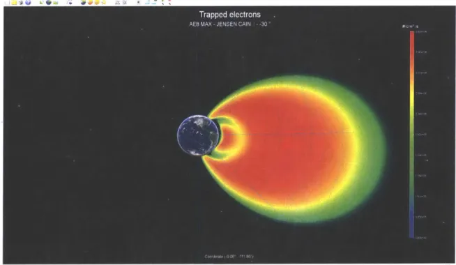
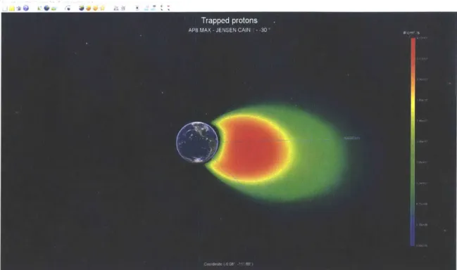
The Van Allen Belts (radiation belts) are toroidal regions of electrons and protons trapped by Earth's magnetic field. The first region, or inner belt, extends from a few 100s of km to ~6,000 km altitude and is dominated by high energy (-10s of MeV) protons, but also contains high energy (1-10 MeV) electrons. The second region, or outer belt, extends out to 60,000 km altitude and is predominately high energy electrons. Figures 2-1 and 2-2 illustrate the structure and integral flux of electrons
and protons.
Figure 2-1: Integral flux of Trapped Electrons generated using OMERE 5.2.2 using the AE8 model for trapped electrons with the Jensen Cain Model, according to
ECSS-10 Standards.
Figure 2-2: Integral flux of Trapped Protons generated using OMERE 5.2.2 using the
AP8 model for trapped electrons with the Jensen Cain Model, according to ECSS-10
Standards.
Neutron Decay) and interplanetary sources (solar wind) and are subject to large temporal variations. The inner belt structure is relatively stable as it is governed
by Earth's magnetic field, but variations correlated with solar cycle and Ionosphere
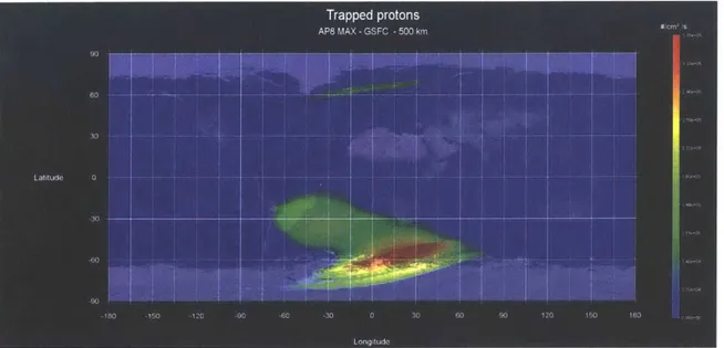
dynamics are seen. The outer belt is more dynamic as it is governed by Earth's fluctuating geomagnetic tail. Earth's magnetic field axis and rotational axis are offset
by an -11-degree northward tilt and 500 km separation. A weaker magnetic field
region results above the south Atlantic near southeast Brazil allowing high energy protons to dip lower into Earth's atmosphere. This region is known as the South Atlantic Anomaly (SAA) and is slowly drifting westward with a period of -1200 years [22]. Figure 2-3 shows increased particle flux levels in the SAA region.
2.1.3
Galactic Cosmic Rays
Galactic Cosmic Rays (GCRs) are the third source of radiation in the near-Earth ra-diation environment. Originating outside of the solar system, GCRs consist primarily
Figure 2-3: Increased proton flux known as the South Atlantic Anomaly at lower latitudes due to the offset in Earth's magnetic field axis and rotation axis.
of high energy protons, heavy ions, and electrons ranging from -1 MeV to 10GeV in energy. These particles interact with Earth's atmosphere and cause Extensive Air Showers (EAS) creating cascades of secondary particles resulting from nuclear interac-tions. These showers of secondary particles consist of high energy neutrons, electrons, and protons and disintegration particles such as pions and muons. GCR activity is inversely proportional to solar activity. During solar maximums, GCR intensity is at a minimum and vice versa. This relationship is attributed changes in the solar wind magnetic field. More turbulent winds present during solar cycle maximums scatter GCRs more effectively and inhibit their propagation to the inner solar system. As the solar winds recede and relax during solar cycle minimums, GCRs more easily penetrate the near-Earth environment.
The Lorentz force from Earth's magnetic field acts as a shield against GCRs (and solar winds). Particles with trajectories parallel to magnetic field lines experience no Lorentz force. The approximate dipole structure of the Earth's magnetic field results in higher levels of atmospheric interaction and particle showers at higher latitudes.
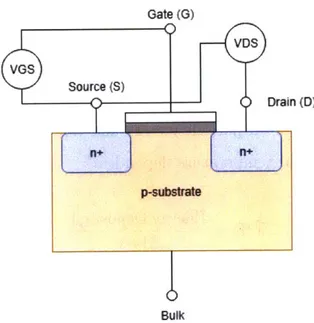
Gate (G) VDS VGS Source (S) Drain (D) n+ n+ Bulk
Figure 2-4: Cross-section and corresponding device representation of a Metal Oxide Semiconductor Field Effect Transistor (MOSFET). The device activitates and allows current to flow between the Drain (D) and Source (S) when the Gate (G) voltage exceeds the voltage between D and S.
2.2
Radiation Effects on Electronics in LEO
Radiation present in the near-Earth environment can adversely affect electronics. Cumulative effects change device operating parameters, degrade performance, and induce leakage currents, while instantaneous or transient events can have destructive or non-destructive effects. A Metal Oxide Semiconductor (MOS) transistor, or
MOS-FET, will be used as a reference device to illustrate these effects. MOSFETs are
the building blocks of modern integrated circuits. While device-level responses may differ for individual MOSFETs in the presence of radiation, using a simple example develops intuition and understanding of the underlying physics.
The basic application of a MOSFET is a voltage-controlled switch and is show in 2-4. By applying a voltage to the gate exceeding the potential between the drain and source, the MOSFET turns on, and current flows between the drain and source nodes. Within the device, voltage applied to the gate creates a conduction channel between the drain and source enabling current flow. These devices are sensitive to both ionizing and non-ionizing radiation.
2.2.1
Total Ionizing Dose
Total ionizing dose (TID) is a cumulative effect caused by incident electrons and protons creating trapped charges within a device. The amount of total charge ac-cumulation or dose depends on particle energy and target material, and the device response to dose is bias and temperature dependent.
TID = Energy Deposited (2.1)
Mass
The underlying physical mechanism of radiation-induced charge trapping happens on picosecond scales. It takes a finite amount of energy to generate electron-hole pairs in a semiconductor. For the purposes of this thesis, its assumed the oxide is SiO2, which has a pair creation energy, EP, of 17 t 1 eV [49]. Incident ionizing radiation in the oxide layer creates electron-hole pairs where the total number of pairs can be determined knowing the incident particle energy, Ep of the material, and the charge
pair volume density per rad go = 8.1E+12 cairsa.
The initial number of charge pairs is a function of the amount of energy imparted to the material by radiation. This value is known as the Linear Energy Transfer (LET) of a particle which is the change in total energy, dE, over the path the particle takes, dx, normalized by the material density p. In particle physics, this is also known as the material stopping power. LET is discussed further in Section 2.2.3. TID can also be expressed in terms of LET.
LET
=
I()
(2.2)p xIonizing
By multiplying LET by the time-integrated integral flux, or fluence
#,
TID can be calculated.TID = #LET (2.3)
In the first few picoseconds following generation, a fraction of the electrons are carried out of the oxide; the remaining electrons recombine with some of the holes to form stable pairs, but several holes remain unpaired. The final number of holes
escaping recombination is a function of the magnitude of the electric field, acting to separate holes and electrons, and the initial number of charge pairs generated by incident radiation. The larger the electric field, the higher the number of holes in oxide layers. Therefore, electronics TID testing involves irradiating both biased and unbiased parts, where biased samples are representative of worst-case charge trapping. In the case of a Negative-channel MOS (NMOS) transistor, a commonly used technology know for its sensitivity to radiation, radiation-induced charge trapping occurs in the gate oxide layer resulting in gate voltage shifts i.e., over time, less voltage is required to create the conduction channel. If the amount of trapped charge is large enough, devices cannot be turned off. Figure 2-5 illustrates MOSFET pre-and post-irradiation operation.
(A) MOS TRANSISTOR - NORMAL OPERATION (B) MOS TRANSISTOR - POST IRRADIATION
BATE FIELD GATE FIELD
OXIDE OXIDE OXIDE OXIDE
SOURCE GATE DRAIN SOURCE GATE DRAIN
CONDUCTING INVERSION POSITIVE OXIDE CHANNEL TURNED CHANNEL (POSITIVE V6) TRAPPED CHARGE ON WITH V6 =0
P-TYPE SILICON P-TYPE SILICON
SUBSTRATE SUBSTRATE
Figure 2-5: MOSFET Operation under nominal conditions
(a)
and post-irradiation (b). Charge accumulates in the gate oxide over time and reduces the amount of voltage required to turn the device on. Eventually, if the cumulative dose is high enough, a permanent conduction channel will form, and the device cannot be turned off even if 0 V is applied at the gate [49].The remaining holes create a bulk charge on the gate oxide, shifting the threshold voltage required to operate the device to a lower level. Other technologies susceptible to TID are other MOS transistors (Complementary MOS, Positive-channel MOS), FETs, integrated circuits (ICs), and bipolar
junction
transistors (BJTs). TID effects in FETs manifest as increased leakage current between the source and drain. Effectsin BJTs result in current gain degradation [49]. Devices utilizing these technologies can exhibit varying sensitivities to TID effects due to variations in process flow (e.g.,
foundry, time of manufacturing). Serendipitously, as device processes shrink, and gate oxide thicknesses and other susceptible device regions shrink, TID tolerance increases as less charge is trapped within critical regions [49].
Both analog and digital components are susceptible to TID as both use sensitive technologies. In the scope of DC-DC converters, TID is expected to mostly influ-ence the switch preceding the inductor in the main circuit and the control circuit monitoring the output (MI and Switching Controls in Figure 1-3).
2.2.2
Displacement Damage
Displacement damage (DD) is the dominant effect for compound semiconductors without oxides to trap charge (e.g., optoelectronics). DD is strictly concerned with non-ionizing radiation effects and can be expressed in terms analogous to TID. The equivalent of LET for DD is known as non-ionizing energy loss (NIEL) which describes the amount of energy imparted to a material causing nuclear displacement.
NIEL = 1
(d)
(2.4)p x)Non-Ionizing
Like TID, the total number of ions through a square centimeter for a given period, or fluence q, multiplied by NIEL gives the total non-ionizing dose contributing to DD.
TNID = ONIEL (2.5)
DD occurs when a crystal lattice nucleus (such as Si) is dislodged by an incident
particle. The displaced atom settles in an interstitial location, and the previously occupied lattice position contains a vacancy. The interstitial atom and vacancy form a Frenkel pair, which is the simplest form of non-ionizing defects [49]. Different materials have different energy thresholds for displacement damage. Table 2.1 lists some common materials susceptible to displacement damage and corresponding DD
energy threshold.
Table 2.1: Displacement damage energy thresholds for common materials susceptible to TNID [49]. Optoelectronics such as photodetectors (PD) will often use these materials.
Material EDD (eV)
Diamond 35 5
Si 27.5
Ge 21
GaAs 7-11
Displacement damage results in defects to the semiconductor bandgap, which can have significant electrical impacts. The first effect is the generation of an electron hole pair from a "center" energy threshold in the bandgap introduced by DD. This process is also viewed as a hole emission followed by electron emission from the center and dominates in regions where free carrier concentrations are less than thermal equilibrium values (i.e., in depletion regions). Increased leakage current is attributed to the introduction of a DD center.
The second effect results in an increased recombination lifetime. The average time a carrier spends in a band before recombining is defined as the recombination lifetime. The defect creates an energy threshold within the bandgap that attracts both electrons and holes, which results in carrier recombination and reduces the time each carrier spends in a band. Gain reduction in bipolar technology is attributed to this mechanism.
The last effect is trap assisted tunneling, wherein carriers tunnel from either the valence or conduction band to the other due to DD-induced defects, creating free charge carriers on both ends. In MOS transistors, the result is higher current levels.
Optoelectrical devices are sensitive to displacement damage as they lack oxides to trap charge induced by radiation [49]. Other sensitive devices include bipolar technologies such as BJTs and MOS transistors. In the scope of DC-DC converters,
DD is not expected to be the dominant radiation-induced degradation and will likely
2.2.3
Single Event Effects
Single Event Effects (SEE) are unwanted or erroneous responses from an electronic device caused by a charged particle passing through the active region of the device. Protons, neutrons, and heavy ions can evoke SEE through direct or indirect ionization mechanisms.
In direct ionization, the charged particle interacts directly with electrons in target material, freeing them from their bound states and leaving a wake known as a charge track. Heavy ion interaction in material typically results in direct ionization as they carry the highest amounts of charge. In indirect ionization, the charged particle interacts with the nuclei of the target material (as in displacement damage), and the recoiling nuclei interact with electrons.
Heavy ions are responsible for mostly direction ionization SEE as they carry the highest amount of charge; additionally, they leave the densest charge tracks of all SEE particles. SEE caused by protons are predominantly the result of indirect ionization, however, smaller process nodes more susceptible to SEE show sensitivity to proton direct ionization. Converse to the improved TID performance, device shrinkage in-creases SEE vulnerability because of reduce charge capacity, and devices operating terrestrially have reported functional disruptions due to SEE [8]. Neutrons solely contribute to indirect ionization as they carry no net charge and do not electrically interact with electrons.
As charged particles interact with a target material, they lose kinetic energy. The linear rate of energy loss is the known as the Linear Energy Transfer (LET) which was mentioned in Section 2.2.1. LET is a function of target material density and the path of the particle through the material (Equation 2.2). The units of LET are energy per unit mass per unit area, or MeV-cm-mg .
It is useful for testing purposes to see LET vs. range curves for a target mate-rial (i.e. how much energy is lost as a function of distance traveled by a particle). The LET vs. range curve reveals the maximum energy lost in a material as well as maximum range of ion and is formally known as a Bragg curve. Figure 2-6 illustrates
10
-Bragg peak
LET
(MeV-cm 2/mg)
1 GeV/amu Neon 0.5 GeV/amu Neon
0.1
0 50 100 150 200 250 300 350 400
Depth in Silicon (mm)
Figure 2-6: Bragg Curve for Neon in Silicon. Initial Energy for Neon is 1 GeV. Bragg
peak occurs at 350 mm [8].
an example of a Bragg curve with a Neon particle incident on a Silicon target ma-terial. Note the maximum range is roughly 350 mm and the maximum LET is ~9.5 MeV-cm 2 -mg'. When the charged particle approaches the region where its kinetic energy is comparable to the imparted energy, LET increases dramatically with range. Initially, the energy lost is low because the velocity of the particle relative to the velocity transferred to the electrons is low. When these values approach equality, a masking effect occurs where the electrons mask the apparent charge of the particle, and the LET decreases dramatically near the end of the ion range [8].
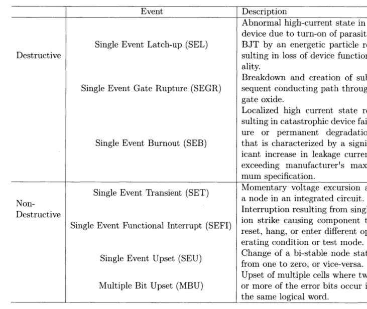
There is a range of behaviors a device may exhibit after a particle hit. Analog and digital devices share some responses, but others are specific to domain. Table 2.2 lists events and device responses broken into two categories: destructive and non-destructive. A non-destructive event implies a device will return to nominal operation after a power cycle or at the end of the upset while a destructive event permanently alters the functionality of the device.
Table 2.2: Single Event Effects Relevant to Hybrid DC-DC Converters
__
I
EventI
Destructive
Non-Destructive
Single Event Latch-up (SEL)
Single Event Gate Rupture (SEGR)
Single Event Burnout (SEB)
Single Event Transient (SET)
SSingle Event Functional Interrupt (SEFI)
Single Event Upset (SEU)
Multiple Bit Upset (MBU)
Description
Abnormal high-current state in a device due to turn-on of parasitic
BJT by an energetic particle
re-sulting in loss of device function-ality.
Breakdown and creation of sub-sequent conducting path through gate oxide.
Localized high current state re-sulting in catastrophic device fail-ure or permanent degradation that is characterized by a
signif-icant increase in leakage current exceeding manufacturer's maxi-mum specification.
Momentary voltage excursion at a node in an integrated circuit. Interruption resulting from single ion strike causing component to reset, hang, or enter different op-erating condition or test mode.
Change of a bi-stable node state from one to zero, or vice-versa.
Upset of multiple cells where two or more of the error bits occur in the same logical word.
For applications requiring stable input voltages, transients could disrupt functionality and lead to gaps in operation. Latch-up events require power resets, also creating potential gaps in operation. In worst-case scenarios, latch-up is destructive and could lead to mission failure.
The SEL mechanism is attributed to the presence of parasitic BJTs within CMOS. Figure 2-7 illustrates a simple CMOS transistor with two parasitic BJTs imposed on the cross section for visualization. A CMOS device consists of several PNP and NPN junctions, each creating a BJT. In the illustrated example, a lateral and vertical BJT
are formed. When a charged particle strikes a CMOS device, track of dense charge is left it its wake. Carriers are swept away and the current spike results in a regenerative
Substrate V Well Contact
_91Contact
p+ n+ ln+ P+ + n+ 7 rbv rev n-well r.1 rbi rs - p-substrate /Figure 2-7: Cross section of CMOS transistor showing parasitic BJTs. Each NPN and
PNP junction creates a parasitic BJT within a CMOS device. When current flows
through these regions, a regenerative gain state is activated, creating a run-away current state. Resistances are from the bulk and substrate materials [8].
gain state of the BJTs. The newly flowing current is met with resistance from the bulk and substrate materials denoted by r,1 and rbl in the lateral BJT and r,, and
rb, in the vertical BJT. The results of this high current state may be destructive as the device fails from thermal effects or cracked dielectrics or non-destructive, which is difficult to prove, as latent damage is often revealed in post-testing analysis [38].
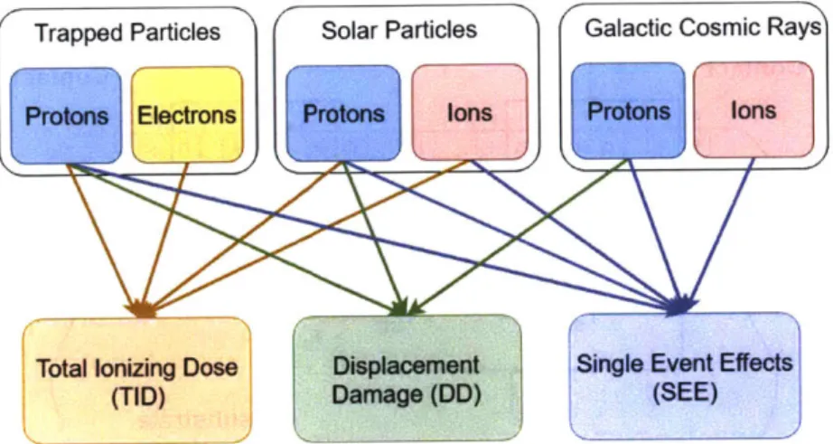
In summary, particles in the LEO radiation environment can cause radiation ef-fects in spacecraft. Particles may have multiple efef-fects depending the on the target device, and particle fluence varies with solar cycle and Earth's magnetic field. Fig-ure 2-8 summarizes the types of energetic particles from key sources and subsequent effects.
2.2.4
Upset Rate Calculations
To quantify the SEE performance of a device, data is required for a known environ-ment configuration. The event cross section, o-, is defined as the expected value of the event rate per flux, or total events per particle fluence. Note the units of a are cm2
,
but a is a probability density function and does not correspond to a physical area. The cross section of a device depends on type of event (e.g., SET or SEL), incident
Trapped Particles Solar Particles Galactic Cosmic Rays
Protons Electrons Protons Ions Protons Ions
Total Ionizing Dose Displacement Single Event Effects
(TID) Damage (DD) (SEE)
Figure 2-8: Summary of energetic particles and radiation effect contributions.
particle energy and subsequent LET, the particle angle of incidence, and circuit test parameters and configuration (e.g., circuit bias, temperature, clock speed, etc.).
Total Number of SEE 2
Particle Fluence (2.6)
Once the cross section is calculated for each event type of interest, it can be plotted against corresponding LET values, creating what is known as the cross-section curve. Figure 2-9 shows a notional cross-section curve. Key parameters of the cross-section curve are the saturation cross section, usat, at which the cross-section saturates (1E-2 in the example curve) and LETonset, which is the lowest LET at which an no events are observed (-2 MeV-cm2-mg-1 in the example curve). The onset LET is also known as the threshold LET.
The cross-section curve can be used to determine the upset rate or event rate for any given orbit. This is critical in developing mitigation strategies and performing failure analyses as it describes the rate at which a device will experience SEE. De-pending on the type of SEE, the failure mode may require a power cycle, so the upset rate may also be used to inform the frequency of power resets. In general, the upset rate is given by Eq. 2.7.
[eventsl
UpsetRate = Flux(orbit) * - ent
1.E-01 1.E-02 Device 1.E-03 g 1.E-04 (cm2) 1.E-05 1.E-06 1.E-07 u- I 1 9 1 0 20 40 60 80 100
Particle LET (Mev-cm2/mg)
Figure 2-9: Notional Cross Section Curve for a device with target material of Silicon. Note the cross section curve is sensitive to ion incident angle [8].
The generalized solution uses - integrated over the LET spectrum of the orbit, which requires a function fit to the data. Early computational models used a step function, however this led to overestimates of event rates due to the additional area introduced by the step-function fit. The solution to better estimates was to apply a cumulative Weibull function to the data.
o-(LET) = osat (I - exp
(
LEToW LET [cm2] (2.8)Where LETO is the onset or threshold LET and width W and shape S are empirical fitting parameters.
It is difficult to obtain cross-section information for all incident angles during testing. Constraints on cost and time prevent collecting incident angle data, and often normal incidence events are used to calculate cross-section. To account for the directional dependence, two rate estimates for each device are calculated to bound the uncertainty: best-estimate, which is representative of realistic mean events, and worst-case, which incorporates margin and is recommended for design purposes. Best-estimate uses the Rectangular Parallel Piped (RPP) model to describe sensitive charge volumes in the device. When ionization from a particle exceeds the charge volume threshold, SEE is induced. RPP is a non-physical model that produces results fol-lowing the cosine law up to angles of 60'. Best-estimate RPP dimensions are set to
![Figure 1-2: Component Grade Spectrum from Texas Instruments [6]. Commercial, Automotive (Q100), Enhanced Performance (EP), and Qualified Manufacturers List](https://thumb-eu.123doks.com/thumbv2/123doknet/14239906.486584/24.917.131.793.124.447/component-spectrum-instruments-commercial-automotive-performance-qualified-manufacturers.webp)


![[PDF] Cours Air : Les vecteurs, les Tests et les matrices | Cours informatique](data:image/gif;base64,R0lGODlhAQABAIAAAP///wAAACH5BAEAAAAALAAAAAABAAEAAAICRAEAOw==)