HAL Id: hal-02135770
https://hal.archives-ouvertes.fr/hal-02135770
Submitted on 21 May 2019
HAL is a multi-disciplinary open access
archive for the deposit and dissemination of
sci-entific research documents, whether they are
pub-lished or not. The documents may come from
teaching and research institutions in France or
abroad, or from public or private research centers.
L’archive ouverte pluridisciplinaire HAL, est
destinée au dépôt et à la diffusion de documents
scientifiques de niveau recherche, publiés ou non,
émanant des établissements d’enseignement et de
recherche français ou étrangers, des laboratoires
publics ou privés.
Theoritical and experimental study of magnetic sensors
for near-field emission measurement. Application to
design and integration in power printed board circuit
Guillaume Viné, Jean-Marc Diénot, Paul-Etienne Vidal
To cite this version:
Guillaume Viné, Jean-Marc Diénot, Paul-Etienne Vidal. Theoritical and experimental study of
mag-netic sensors for near-field emission measurement. Application to design and integration in power
printed board circuit. International Symposium on Electromagnetic Compatibility, EMC Europe
2017, Sep 2017, Angers, France. pp.0. �hal-02135770�
OATAO is an open access repository that collects the work of Toulouse
researchers and makes it freely available over the web where possible
Any correspondence concerning this service should be sent
to the repository administrator: tech-oatao@listes-diff.inp-toulouse.fr
This is an author’s version published in:
http://oatao.univ-toulouse.fr/21714
To cite this version:
Viné, Guillaume
and Diénot, Jean-Marc and Vidal,
Paul-Etienne
Theoritical and experimental study of magnetic
sensors for near-field emission measurement. Application to
design and integration in power printed board circuit. (2017)
In: International Symposium on Electromagnetic Compatibility,
EMC Europe 2017, 4 September 2017 - 8 September 2017
(Angers, France).
Official URL:
https://doi.org/10.1109/EMCEurope.2017.8094622
Abstract – For electromagnetic interaction analysis in power
electronics, the study and the design of Near-Field integrated magnetic antennas are presented. An antenna model is developed and compared to experimental data. The modeling and the performances of the prototype is discussed in function of the source position and the antenna design.
Keywords—magnetic sensor; near-field; emission; radiation; PCB; Power PCB;
I. INTRODUCTION
New developments in power electronic design deals with power density, switching ranges and more generally with wide band gap semiconductors’ integration. This trend accentuates the Electromagnetic Compatibility (EMC) issues. More precisely, high levels of conducted and radiated disturbances are concerned and can degrade the overall device efficiency [1]. As a way of consequence, from the design stage, it is interesting to characterize these non-desired contributors.
Near-Field (NF) techniques enable the development of non-intrusive sensors with high temporal and spatial resolution [2]. The electric field measurement is ensured by monopole and dipole probes whereas loop probes are used for magnetic field measurement [3]. In most applications, these sensors are associated with an external motorized arm to scan step after step the top surface of the Device Under Test (DUT). That gives access to electromagnetic (EM) cartography. Indeed, the localization of EM radiation sources and the DUT currents estimation is performed [4]. The sensor efficiency depends on probe size, area of the DUT and on the resolution step of the scanning system. However, the main drawback of NF scanning technique is the time consumption to collect all the samples, especially in Power Printed Circuit Board (PPCB) and Hybrid 3D structures. Due to their large size and to the 3D top surface, the scanning step and time characterization of such measurement systems does not allow an “in situ” and real time measurements
To overcome this drawback, the solution developed in this study is based on sensor integration onto the given electronic module, as started in [5][6]. First prototypes of magnetic probes are studied in this paper. Firstly, principle of magnetic NF antenna and main measurement issues are addressed. Next, the reference antenna prototype is presented. The model developed is detailed and validated according to experimental results. The antenna is characterized in coupling and the measurement issues
are evaluated. Finally, two prototypes are studied to highlight the influence of ground plane and electric shield.
II. NEAR FIELD MEASUREMENT FOR POWER ELECTRONIC DEVICES
A. Near field principle
In electrical circuits, the EM field exists due to current flows and potential variations. In power modules, it has been demonstrated that high currents and voltages associated with very short switching times cause wideband EM radiations until 1 GHz [7]. Close to sources, magnetic and electric fields are decoupled and one of them is dominant: the magnetic field for current flows, the electric field for potential variations [8]. This corresponds to the NF region defined by (1) with D the distance between source and antenna, f the signal frequency and v the speed of light through the propagation medium.
< 2
(1) The NF measurement in power modules requires a high proximity to the emission sources. For instance, a 1 GHz frequency signal through the vacuum, corresponds to D=5 cm limit distance. Antenna integration is well suited to this condition.
B. Magnetic antenna
Among elementary probe technologies, the Fig.1 illustrates the sample which will be used in this study. It corresponds to a loop antenna printed on FR4 epoxy substrate with RSthe radius from the center of the loop to the middle of the trace, tsthe trace thickness and dsthe trace width.
It operates on the principle of inductive coupling according to Lenz's law (2). The change of the magnetic flux Φ through the loop surface S induces an electromotive force e at its terminal. Obviously, the magnetic flux is linked to the radiated magnetic field ⃗.
= − , = ⃗. ⃗ (2)
Following the ratio between the antenna radius and the distance of the magnetic source, the ⃗ field is considered homogeneous inside the loop. Then, the electromotive force is deduced. It is expressed following the normal component of the magnetic field at the antenna center (3).
Theoritical and Experimental Study of Magnetic
Sensors for Near-Field Emission Measurement.
Application to Design and Integration in Power Printed Board Circuit.
G.
Vine
1, J.-M.
Dienot
2,
P.-E.Vidal
11 LGP EA1905, Ecole Nationale d'Ingénieurs, INPT, Tarbes, France, guillaume.vine@enit.fr 2 LGP/Labceem, Université P. Sabatier, Tarbes, France, jm.dienot@iut-tarbes.fr
Fig. 1. Ideal design of the loop antenna with PCB technology
= ≈ ∗ (3)
It is noted that the cross-sectional dimensions of the trace are also a source of uncertainty. That can modify the magnetic field captured by the antenna as explained in [9] and so disturb the measurement. Based on that, the antenna radius is chosen as ≫ { , }and its influence is considered negligible: Rs=3
mm, ts=0.035 mm, ds=0.2 mm. The substrate thickness is 1.6
mm.
Finally, the measuring device accesses to the voltage across the loop through access lines, as shown in Fig. 2. It is noted that the whole measurement chain affects the antenna response. The antenna factor Fm is defined in (4). It includes all the measurement chain: the loop, the transmission line and the measuring device symbolized as an output resistance RM[10].
= (4)
VMcorresponds to the voltage across RM. The antenna factor characterizes the sensitivity of the antenna and needs to be maximized for measurement efficiency.
Fig. 2. Measurement chain of the real design of the magnetic probe. C. Measurement conditions
The equation (3) requires two ideal assumptions about the antenna that can derive errors in the values measured during the characterization process. The antenna should be a punctual receiver, and the antenna should only detect the magnetic field. To fulfill these requirements, an analysis on the design and the positioning of the antenna are done in order to ensure the reliability of the measurement. They are detailed further in the paper.
1) Punctual receiver
In the near-field environment, the extremely non-uniform spatial variation of the magnetic field can induce large error due to the integrating effect of the antenna [11]. However, reducing these dimensions affects the amount of flux picked up by the
antenna. Consequently, spatial precision comes at the expense of sensitivity.
2) Electric field rejection
The antenna receives power associated to the electric field PEand magnetic field PH[12]. In order to consider the antenna as a magnetic sensor, PEhas to be negligible compared to PH. This corresponds to the electric field rejection of the antenna. The antenna sensitivity to the electric field mainly impacts at high frequencies but can greatly disturb the magnetic field measurement.
In the following, the electric field rejection will be studied for a transmitting antenna/receiving antenna system with the power transfer parameter S21.
D. Antenna Design
A first antenna prototype including the loop and the access lines is presented in Fig.3. The antenna is connected to the measuring instrument by a SMA connector and SMA cable of 50 Ω characteristic impedance. The loop and cross-sectional trace dimensions were presented previously. The length of the access lines is chosen at La=15 mm and the spacing from inner edges at ΔL=0.3 mm.
Fig. 3. View of the PCB antenna prototype.
III. ANTENNACHARACTERIZATION
An antenna model based on this prototype design is done. As it is designed for power electronic modules, its model and its characterization are developed and studied out over the frequency range 1 kHz-1 GHz. This corresponds to the frequency band of power modules EM interactions.
A. Antenna modeling
To correspond with the electrical behavior, the antenna is divided in 3 parts: the loop, the transmission line and the connector. The dimensions of each part allow considering the quasi-static approximation inside them over the studied frequency range. Each parts are so modeled by an equivalent RLCG circuit. Finally, a complete model is established and presented in Fig. 4. The couplings between the three parts are inserted as mutual inductances and capacitors. The measuring device is included and is represented by the input voltage Vinand the termination load RM=50 Ω. The magnetic coupling is represented by the electromotive force e.
Values of electrical parameters and coupling coefficients, among the frequency, are extracted with 3D Numerical Tool Q3D Extractor®[13].
Loop
-Fig. 4. Lumped parameter circuit of antenna B. Antenna model validation
The objective is to validate the equivalent input impedance of the antenna. Consequently, the antenna impedance is computed from the lumped model established previously and compared to the measurement.
For that, the electromotive force e is considered zero. The circuit is then transcribed in an equation system based on the Kirchhoff’s voltage laws. Each independent mesh corresponds to an equation. A nine-equation system is obtained. The input of the system is Vinand the outputs are some branches currents highlighted Fig. 4. The system is solved in the frequency domain. Indeed skin effects and eddy currents are taken into account. Finally, the input impedance is calculated from the current I1:
= − ∗ (5)
A Vector Network Analyser (VNA) is used to validate the modeling. It enables to measure the input impedance of the antenna. The calibration of the measurement is carried out with a Short-Open-Load kit. The antenna is 0.5 m away from any metal object to avoid coupling. The electromotive force induced by magnetic coupling can be supposed negligible. The calculated values and the measurements are represented in Fig. 5.
Fig. 5. Calculated and Measured Input impedance of the prototype 1
A good agreement between the input impedance model and the impedance measurement is observed over the studied
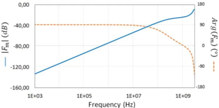
frequency range. This result will help to plot the antenna factor. Consequently, the antenna factor can be computed. To do so, the antenna is considered in reception mode. The input of the system is now the electromotive force e, induced by magnetic field through the antenna (3) and Vinis considered zero. In such mode, the output of the antenna corresponds to the voltage VM across the termination load RM=50 Ω. The antenna factor is deduced from (4) and plotted in Fig. 6.
Fig. 6. Antenna factor of the prototype 1
The cutoff frequency of 3 dB deviation is identified @230 MHz. The linear response of the antenna is thus over the frequency range below 230 MHz.
C. Coupling model
The coupling between two coplanar antennas, as source and receiver, is studied now. Magnetic and electric couplings will be evaluated to characterize the electric field rejection of the receiver antenna. The geometrical characteristics of the antennas are identical. Fig. 7, illustrates the coupled antennas. dais the distance between the antennas, Cpthe parasitic capacitor due to electric coupling and Mpthe mutual inductance due to magnetic coupling.
Magnetic and electric couplings are modeled separately in Fig.8. They are based on the previous antenna model with the addition Cp and Mp. NF couplings are calculated with the software Ansys Q3D Extractor®.
Fig. 7. Geometry of the Antenna coupling
(a) e 0,00 180 CmJ /9 ::i:. ,-.. -40,00 90 -; Q:)
-...
C<::, '"Cl--
,-.. .._,--
-
;l"'r]-cl
-80,00--
-
0 .._,-
,-.. ' \ .._, 0 I I -120,00 I -90 -160,00 -1801E+03 lE+0S 1E+07 1E+09
Frequency {Hz) 1E+04 1E+03 ,-.. 1E+02 C: Source Receiver ...., .: .__, .: 0 N lE+0l <1>- -~...., <1>.::l lE+OO l--;:; ;:; '-' lE-01
---c,,~Cl Cl 1E+03 lE+0S 1E+07 1E+09
<Ii (J ~~ 90 ~ "Cl :;:::; 0 ,-.. 45 ::,,.~ 0 .__, N 0
---bJ) :-C1l -45 -90 I I1E+03 1E+05 1E+07 1E+09
Frequency {Hz)
(b) Fig. 8. Coupling models, (a) magnetic, (b) electric
The S21 parameter between the source and the receiver expressed in (6), corresponding to the power transfer, is simulated with the magnetic and electric coupling model of Fig. 8 for da=2 mm. VM2 and Vin1 are the voltage across the
termination load of the receiver antenna and the input voltage of the source antenna respectively.
21 =2 ∗ (6)
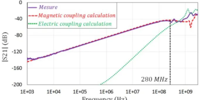
The results obtained are compared to the VNA measurement in Fig.9. To do so, the calculation of the parasitic capacitor and the mutual inductance gives: Cp=144 fF and Mp=255 pH.
Fig. 9. Power transfer between the loop antennas (da=2 mm)
The comparison between the magnetic coupling and electric coupling calculation allows to identify an electric field rejection insufficient above f20dB=164 MHz. This is confirmed by the VNA measurement. Indeed, a good agreement with the magnetic coupling calculation is observed below this frequency and similarities with the electric coupling calculation are observed beyond it. The electric field rejection is not ensure at high frequency. This constrains the frequency measurement band of the antenna.
The influence of the distance to the source on the measurement conditions is studied in the following.
D. Measurement conditions analysis 1) Electric field rejection
The parasitic capacitor and the mutual inductance are calculated depending on the distance da and reported in Fig.10. The parasitic capacitor decreases less rapidly than the mutual inductance. Thus, the electric field rejection factor increase as a function of the distance and the measurement frequency band is reduced. This is confirmed by the VNA measurement. Fig. 11 shows the S21 measurement for different distance to the source. For example, at 14 mm, the magnetic coupling domain is
reduced below 70 MHz. The low-frequency bearing
corresponds to the noise threshold of the VNA.
Fig. 10. Parasitic capacitor and mutual inductance calculation in function of the distance to the source (f=1 GHz)
Fig. 11. Power transfer measurement in function of the distance to the source Thus, an electrical shield must be studied for wideband measurement until 1 GHz.
2) Punctual receiver
The dimensions of the loop are also a source of measuring error due to magnetic field non-uniform variation. The spatial error is defined in (8) with ϕ the magnetic flux through the antenna defined in (2), HnO the normal component of the magnetic field at the antenna center and RSthe radius of the loop (Fig. 1).
= − ∗ ∗ ∗
∗ ∗ ∗ (7)
ϕ and HnO are calculated theoretically with the Biot and Savart law as in [11]. The spatial error is reported in Fig. 12, in function of the distance d to the source.
Fig. 12. Spatial error of magnetic field evaluation in function of the distance to the source
The spatial error is thus important near the source. The antenna radius must be small compared to the distance to the source. This is done to the detriment of the sensitivity.
ai' ~ ,-< N ~ 0 -40 -80 -120 -160
lLoop1 RLoop1 LLoop2 RLoop2
---n2
/
:
,
Cp
u
•
:
2
---f
~ ~f
~ ...
!
...!
... ~ '-I---
---lLoovJ RLoop1 lLoop2 RLoop2
2 2 2 2 Antenna 1 Antenna 2 - Mesure ---Magnetic coupling calculation ' i.•· _
..
···' ···/ 164 MHz -2001E+03 1E+o4 lE+OS 1E+06 1E+07 lE+OB
Frequency (Hz) ,,...., co :2, r l N ~ 1E+09 E l,SE-13 l,2E-13 6E-14 0 ' ' ' ' ' ',,, __________________ _
---4,5 9,5 12 14,5 da (mm) O ~l-- ·-2m_m ___ S_m_m ___ 7_,_S_m_m ___ l_O_m_m _ __ 1_4_m~ml -40 -80 -120 -1601E+03 lE+OS 1E+07
Frequency (Hz) 0,2 0,15 0,1 0,05 0 8 13 18 23 cla (mm) 2,7E-10 l,SE-10 9E-ll 0 1E+09 28
IV. INFLUENCE OF THE PROBE’S DESIGN
The antenna optimization depends of the source geometry and the design of the antenna. So, the surrounding environment as a ground plane or an electric shield influence the performance of the antenna. Two other prototypes are studied for this, where dimensions of the loop and access lines are the same as the prototype 1. The first one integrates a ground plane on the bottom of the substrate, with a 0.035 mm thickness, and a 1.6mm distance of the loop. The dimensions are 1.2cm x 3.3cm, that cover the entire sensor. The second one has a guard ring on the top of the substrate (Fig.13). The spacing between the loop and the guard ring, from inner edges, is = 0.3 . It is known that the insulation of the guard ring increases with its width [14]. The main limit overcomes with the increase of the antenna crowding, which can be restrictive in a high-density power
module. A small width of = 0.2 is studied here. The
ring is cut at the extremity of the antenna to avoid current circulation in the ring due to magnetic field.
Fig. 13. View of the PCB antenna prototype 2 (with guard ring)
The ground plane and the guard ring impact onto the antenna measurement behavior will be highlighted. The antenna prototypes 2 and 3 are firstly characterized and compared to the prototype 1.
A. Antenna Characterization
The antenna model is updated by a new calculation of lumped parameters with the software Q3D Extractor®. The
model calculation and the impedance measurement are compared, for prototypes 2 and 3, in Fig. 14 and Fig. 15, respectively.
Fig. 14. Input impedance of the prototype 2
Fig. 15. Input impedance of the prototype 3
The antenna factors are so calculated. The antenna factor of the prototype 2 and 3 are compared to the prototype 1, in Fig. 16.
Fig. 16. Antenna factor comparaison between the prototype 1 and the prototypes 2 and 3
A shift less than 1 dB is observed for the two prototypes below 600 MHz. Over the frequency range of 500 MHz-1 GHz, the impact of the ground plane and the guard ring can be linked to the resonances shifts of the input impedance. They disturb the looping magnetic field and reduces the sensitivity of the antenna, as explained in [15]. A correct magnetic field evaluation is harder around the resonance frequencies identified in Fig. 5, Fig. 14 and Fig. 15: 1 GHz for the prototype 1, 800 MHz for the prototype 2 and 850 MHz for the prototype 3. Then, for a wideband measurement until 1 GHz, the presence of the ground plane and the guard ring must be specially considered.
B. Impacts on the Coupling models
We consider now the shifts on the coupling's parameters of the prototypes. At the critical frequency of 1 GHz, calculations of the mutual inductance Mpand the parasitic capacitor Cpat 1 GHz show a great decrease of Cp=24 fF, and a smaller decrease of the Mp=155 pH. According to that, the ground plane reduces the magnetic coupling with the source at high frequency but increases the electric-field rejection. Indeed, the ground plane modifies the orientation of the magnetic field due to eddy currents and skin effect [16], and improves electrical immunity. For the guard ring, the calculation shows a division by 2 of the parasitic capacitor Cp=74 fF, the mutual inductance is identical.
1E+04 1E+03 ,-, 1E+02 C: ...., ;= ' - ' ;= 0 lE+0l
'"'
·-
N 1: ...., lE+00 '"'..:cl .... ;:l ;:l '-' lE-01"'~
c:l c:l 1,00E+03 1,00E+05 1,00E+07 1,00E+09
'"'c._, ~~ 90 <s: "c:l ~ <: 0 45
,,
,,
:::,..~ ,-, t_..,,,
,,
N 0,,
I bJJ I,..
I ell I -45 I I I I -901E+03 1E+05 1E+07 1E+09
Frequency (Hz) Gap-Frequency (Hz) 1E+04 1E+03 ,-.. 1E+02 C: ...., ~ .._., lE+0l ~ 0 N
'"'·-1: ...., lE+OO '"'..:cl .... ;:l lE-01 ;:s '-' v,~ 1E+03 1E+05 1E+07 1E+09 c:l c:l '"'c._, ~~ 90 s::i: "c:l <: 0 :::,..~ ,-.. 45 0 .._., N 0 b.O,..
ell -45 -901,00E+03 1,00E+05 1,00E+07 1,00E+09
The relative important value of the capacitor is due to the small width of the guard ring. The electric field rejection can be improved by increasing it.
Finally, the S21 parameters from the prototype 1 to prototype 2 and from the prototype 1 to 3 are measured and compared to the results obtained by the coupling models, in Fig. 17 and Fig. 18 respectively. The precision of the modeling is reduced by the complexity of the system. It mainly impacts the electric coupling which does not match with measurements. However, the S21 measured is in good agreement with the magnetic coupling calculation above 450 MHz for the antenna with ground plane and 280 MHz for the antenna with guard ring. The increase of the rejection is thus well observed in experimentation.
Fig. 17. Power transfer measurement and calculation of prototype 2
Fig. 18. Power transfer measurement and calculation of prototype 3
To conclude, the influence of the ground plane is identified as reducing the magnetic couplings, increasing the electric field rejection and shifting the antenna resonances towards the low frequencies. The influence of the guard ring is identified as increasing the electric field rejection and shifting the antenna resonance towards the low frequencies but also increasing the antenna crowding.
V. CONCLUSIONS
The main measurement issues of loop antenna were
identified and addressed. A prototype of antenna dedicated to the power module measurement was presented. A wideband model was developed and characterized and the antenna factor calculation was done. The electric field rejection was identified to be problematic at high frequency (>100 MHz). The influence of the distance between the antenna and the source was presented and shows a competition between performance criteria. The impact of ground planes and guard rings were discussed. Finally, the validation of antennas model and design allows us to integrate them onto real power modules. Indeed, an
in-situ near magnetic field will be achieved.
Acknowledgment
This study is funded and supported by the French National Research Agency for Science, with the Project CAPTIF -Embedded innovative sensors and software in power electronic components - ANR-14-CE05-0044.
References
[1] A. Domurat-Linde and E. Hoene, "Investigation and PEEC based simulation of radiated emissions produced by power electronic converters", in Proc. of 6th International Conference on Integrated Power Electronics Systems(CIPS), pp. 1-6. Nuremberg, 2010. [2] D. Baudry, A. Louis, and B. Mazari, "Overview of emission and
susceptibility investigation and modeling with near-field measurements", in Proc. Gen. Assembly Int. URSI , Chicago, IL, 2008.
[3] H. Funato and T. Suga, "Magnetic near-field probe for GHz band and spatial resolution improvement technique", In Proc. of 17th International Zurich Symposium on Electromagnetic Compatibility, pp. 284-287, Singapore, 2006.
[4] T. Dubois, G. Duchamp, J. Weckbrodt and S. Azzopardi, "Near-field scan tools for embedded electronic analysis", Pan Pacific Microelectronics Symposium, pp. 1-9, Big Island, HI, 2016. [5] G. Lourdel, E. Dutarde, J.M. Dienot, "System for Measuring an
Electromagnetic Field, A Control Sytem Using The Measuring System, and an Electronic Circuit Designed for The Measuring
System", International Patent AG01R3300FI, Number
20009016043, Alstom Transport S.A., June 25th, 2009.
[6] J. M. Dienot and E. Batista, "EM-Matrix antenna for real-time measurements of electromagnetic noise in power electronic modules," in Proc. of Antennas & Propagation Conference, LAPC2009, pp. 753-756, Loughborough, UK, 2009.
[7] R. Redl, "Electromagnetic environmental impact of power electronics equipment", in Proceedings of the IEEE, vol. 89, no. 6, pp. 926-938, June 2001.
[8] V. Kraz, "Near-field methods of locating EMI sources" Compliance Engineering Magazine, n° 6–7, May–June, 1995.
[9] C. F. M. Carobbi and A. Bonci, "Electromotive Force Induced in and Inductance of an Electrically Small Circular Loop Antenna," in IEEE Transactions on Electromagnetic Compatibility, vol. 56, no. 4, pp. 780-783, Aug. 2014.
[10] M. Ishii and K. Komiyama, "A Measurement Method for the Antenna Factor of Small Loop Antenna by Measuring the Input Impedance", in Proc. of Digest of Conference on Precision Electromagnetic Measurements, pp. 80-81, London, 2004. [11] Funato and T. Suga, "Magnetic near-field probe for GHz band and
spatial resolution improvement technique", in Proc. of 17th
International Zurich Symposium on Electromagnetic Compatibility, pp. 284-287, Singapore, 2006.
[12] H. Whiteside and R. King, "The loop antenna as a probe," in IEEE Transactions on Antennas and Propagation, vol. 12, no. 3, pp. 291-297, May 1964
[13] http://www.ansys.com/products/electronics
[14] Salman, R. Jakushokas, E. G. Friedman, R. M. Secareanu, and O. L. Hartin, "Methodology for Efficient Substrate Noise Analysis in Large Scale MixedSignal Circuits", IEEE Transactions on Very Large Scale Integration (VLSI) Systems, Vol. 17, n°10, pp. 1405-1418, October 2009.
[15] Jung-Min Kim, Woo-Tae Kim and Jong-Gwan Yook, "Resonance-suppressed magnetic field probe for EM field-mapping system", in IEEE Transactions on Microwave Theory and Techniques, vol. 53, no. 9, pp. 2693-2699, Sept. 2005.
[16] C. V. Dodd, W. E. Deeds, J. W. Luquire, and W. G. Spoeri, "Some Eddy-Current Problems and Their Integral Solutions", Rept. No. ORNL-4384, 1969 0 - Mesure -40 ,--.. -80 co ~ ...-< -120 N ~ -160 -200 ---Ma911etlc coup/1119 calculaUon _.:··.
••••• Hlectric couplln,q calculation -- -.. -.. "' .. ~'": ·"'·
'='
-
·
-~/
.. •····
:
....
·....
!
....
···:
.--····....
!
,•• I ... ,/ 450 MHzI
1E+03 1E+04 lE+0S 1E+06 1E+07 1E+08 1E+09
Frequency (Hz)
0
-40
- Mesure
---Magnetic coupling calculation ,--.. -80 co ...
-
~
---~'""'.;c
,
_,,
...
···:••' ,: ~ ...-< -120 N ~ -160 -200...
///···
::~M
H
,
1E+03 1E+04 lE+0S 1E+06 1E+07 1E+08 1E+09