HAL Id: hal-02457976
https://hal.archives-ouvertes.fr/hal-02457976
Submitted on 28 Jan 2020HAL is a multi-disciplinary open access
archive for the deposit and dissemination of sci-entific research documents, whether they are pub-lished or not. The documents may come from teaching and research institutions in France or abroad, or from public or private research centers.
L’archive ouverte pluridisciplinaire HAL, est destinée au dépôt et à la diffusion de documents scientifiques de niveau recherche, publiés ou non, émanant des établissements d’enseignement et de recherche français ou étrangers, des laboratoires publics ou privés.
inteGrating 5G Networks (WONG5)
Sylvain Traverso, Rafik Zayani, Hmaied Shaiek, Christophe Alexandre, Daniel
Roviras, Jean-Baptiste Doré
To cite this version:
Sylvain Traverso, Rafik Zayani, Hmaied Shaiek, Christophe Alexandre, Daniel Roviras, et al.. Wave-forms MOdels for Machine Type CommuNication inteGrating 5G Networks (WONG5). 2019. �hal-02457976�
Waveforms MOdels for Machine Type CommuNication
inteGrating 5G Networks
(WONG5)
Document Number D5.2
Software Defined Radio demonstrator specifications
Contractual date of delivery: 15/01/2019
Project Number and Acronym: ANR-15-CE25-0005, WONG5
Editor: Sylvain TRAVERSO (TCS)
Authors: Sylvain TRAVERSO, TBD (TCS)
Rafik Zayani, Hmaied Shaiek, Christophe Alexandre, Daniel Roviras (CNAM)
Participants: TCS / CNAM
Workpackage: WP5
Security: Public (PU)
Nature: Report
Version: 1.3
Abstract:
This report presents the specifications of the demonstrator developed in order to assess the performance of the four selected waveforms in front of realistic transmitter RF impairments. The demonstrator will be capable to address low and high transmitted power scenarios using two different types of Power Amplifiers (i.e. 1W and 10W crest powers). The use of signal processing algorithms (PAPR reduction and DPD) will be evaluated in order to improve the PA efficiency.
Document Revision History:
Version Date Author Summary of main changes
0.0 27.09.2018 S. TRAVERSO Initial structure of the document
0.1 12.10.2018 S. TRAVERSO Modification of the table of content
1.0 15.10.2018 R. Zayani, H.
Shaiek, C. Alexandre, D.
Roviras
CNAM contribution added
1.1 25.01.2019 R. Zayani, H.
Shaiek, C. Alexandre, D.
Roviras
CNAM contribution (update)
1.2 29.05.2019 S. Traverso TCS contribution
Index
1 Introduction ... 6
2 Demonstrator overview ... 7
3 PA-1W based demonstrator specifications ... 9
3.1 Overall Architecture ... 9
3.2 Software Architecture ... 9
3.3 Hardware Architecture ... 12
3.4 PA-1W based demonstrator: Operating mode ... 16
4 PA-10W based demonstrator specifications ... 19
4.1 Overall Architecture ... 19
4.2 Software Architecture ... 19
4.3 Hardware Architecture ... 21
4.1 PA-10W based demonstrator: Operating mode ... 22
5 KPI ... 23
6 Conclusion ... 24
References ... 25
1 Introduction
This second deliverable of work package 5 aims to describe the demonstrator specifications. In WONG5, we choose to address the performance of the selected multicarrier waveforms (CP-OFDM, WOLA-OFDM, and f-OFDM) for both low-power (1W) and high power (10W) transmitters. These transmitters will experience different kinds of imperfections so that different types of digital compensation algorithms (i.e. PAPR reduction and DPD) will be developed accordingly.
In this deliverable, we will first present the demonstrator overview in section 2. Then, we will focus on the specifications of the low-power (section 3) and high-power transmitter (section 4) demonstrators. KPI will be reviewed in section 5 and conclusions will be drawn in section 6.
2 Demonstrator overview
In WONG5, we aim to analyze and compare the performance of the selected waveforms in a context of MTC. More specifically, the demonstrator will address the following topics:
- Case 1 : impact of power amplifier (PA) on the PSD, EVM and BER on the transmitted signal,
- Case 2 : impact of time/frequency asynchronism between two users.
The block diagrams of the demonstrator are presented in Fig. 1 for case 1 and Fig. 2 for case 2. PC Matlab USRP Radio Frequency PA Radio Frequency USRP User of interest Reception Signal of interest (Baseband) Feedback signal for DPD learning (Baseband)
Signal for analysis (Baseband)
Signal of interest (RF)
Figure 1: Block diagram of the WONG5 demonstrator for case 1
PC Matlab USRP Radio Frequency Radio Frequency USRP
User of interest + Interferer
Reception of signal of interest Signal of interest
+ Interferer signal
(Baseband)
Signal for analysis (Baseband)
Signal of interest + Interferer signal
(RF)
The demonstrator is composed of
- A PC which is in charge of all the digital processings, i.e. modulation and demodulation, synchronization, PAPR reduction, Digital Predistortion, signal analysis (BER, EVM, …). Note that all the processings are performed off-line using I/Q patterns.
- USRP boards for the transmission/reception of the I/Q patterns.
- Radio Frequency components for the frequency transposition, filtering, pre-amplifying the signal, etc…
- Two types of PA will be used. The use of efficient PA usually requires complex and potentially energy hungry digital signal processings in order to ensure sufficient linearity. In WONG5, we will consider two types of PA corresponding to two different strategies in order to assess which strategy is the most efficient one, taking into account the global consumption of the transmitter:
o A low efficient PA but easy to linearize o A very efficient PA but hard to linearize
To demonstrate the impact of time and frequency asynchronism between two users in a controlled environment, two signals (user of interest, and Interferer) will be generated digitally (i.e at the baseband level). In this environment it will be possible to finely manage the timing offset between the two users. These results will be compared to the numerical simulations performed in WP 2. Therefore, in this controlled environment, the impact of the PA on the receiver performance will be not assessed.
3 PA-1W based demonstrator specifications
3.1 Overall Architecture
In order to evaluate the performance of the selected MWFs, testbed experiments are done in a realistic laboratory-like environment using configurable universal software radio peripherals (USRPs) based software defined radio (SDR) prototype.
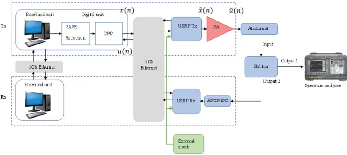
The SDR testbed consists of with two parts, Transmitter (Tx) and Receiver (Rx), to evaluate the performance of several MWFs. The testbed overall architecture is presented in Fig. 3. The baseband unit is software-based and implemented using MATLAB and it realizes the digital algorithm, e.g., waveform generation, QAM modulation, channel equalization, demodulation, etc. It is worth mentioning that digital predistortion (DPD) and peak-to-average power ratio (PAPR) reduction methods are also implemented using MATLAB.
Figure 3: Overall architecture of 1W based demonstrator
3.2 Software Architecture
In order to ensure a real-time SDR implementation, we consider a specific computer configuration (see Fig. 4) using two computers.
The computer 1 has two solid state drives (SSDs), where the first SSD is dedicated to the operating system while the second one is devoted to data storage and is shared with computer 2 using Network File System (NFS) protocol through a gigabit Ethernet interface. It is worth to point that the reason to use SSDs is related to the fact that they are typically faster and more reliable than hard disk drive (HDD) improving performance of frequently accessed data.
𝑥(𝑛) 𝑥̃(𝑛)
𝑢(𝑛)
Figure 4: Computer architecture
MATLAB on computer 1 realizes the digital algorithms, like waveform generation, PAPR reduction and DPD and updates the files containing the transmit signal (‘To_usrp’) and the side information (‘SI’) that will be used by the receiver side. ‘To_usrp’ and ‘SI’ are stored in the second (shared) SSD. Then, GNU-radio configures and uploads ‘To_usrp’ signal to USRP Tx.
Also, a C++ program is implemented in computer 1 to get the received signal from the USRP Rx (‘From_usrp’). This received signal is splitted into small packets that will be stored in the second (shared) SSD and will be analyzed in the baseband unit at the receiver side.
Both USRP Tx and USRP Rx are communicating with computer 1 through another gigabit Ethernet interface (see Fig. 4). Therefore, we consider a sampling frequency (Fs) of 10 MHz leading to a full-duplex transmission rate of about 640 Mbps that will comply with the used gigabit Ethernet interface.
Computer 2 realizes the analysis of received signals. It uses shared received packets and gives some visual performance results such as PSD, constellation, NMSE per subcarrier, average NMSE and BER.
Two graphical interfaces have been developed to make our testbed more flexible (see Figs. 5 and 6). On the transmitter side interface, we can choose different configurations, for example, we can select the waveform (CP-OFDM, WOLA-OFDM or BF-OFDM), the input back-off IBO (0, 3, 6, 9 or 12 dB), the PAPR reduction method (TR or SLM), the DPD and we can enable or disable the interferer user. The receiver interface is dedicated to visualize performance results for these different configurations.
It is worth to mention that we have considered an additive white Gaussian noise (AWGN) channel without any frequency selectivity in order to clearly see the impact of the RF PA on the performance of the selected MWFs and their robustness to asynchronous transmissions.
We recall that the RF PA is a solid-state power amplifier (SSPA) PE15A4017 from Pasternack as described in section 3.1.
Using this Testbed, we aim to evaluate the capability of the selected MWFs (i.e., CP-OFDM, WOLA-OFDM and BF-OFDM): (1) to resist to the distortions caused by the RF PA while keeping good energy efficiency and (2) to support asynchronous multi-user access.
Figure 5: Transmitter interface
3.3 Hardware Architecture
Figure 7 illustrates the different equipment used for the development of the WONG5’s demonstrator.
Figure 7: Testbed Equipment
3.3.1. URRP modules
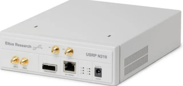
For SDR hardware, two separate Universal Software Radio Peripherals (USRPs) devices, NI-USRP-2942R (Fig. 8) & USRP-N210 (Fig. 9) are used as transmitter and receiver, respectively [2].
Figure 8: NI USRP-2942R
At the transmitter side, we adopt a USRP-2942R module that provides an integrated hardware and software solution for rapidly prototyping high-performance wireless communication systems. Thus, we can prototype faster and significantly shorten time to results. You can prototype a wide range of advanced research applications that include
Attenuator + Splitter USRP Tx USRP Rx PA Attenuator External clock Tx Rx
multiple input, multiple output (MIMO); synchronization of heterogeneous networks; LTE relaying; RF compressive sampling; spectrum sensing; cognitive radio; beamforming; and direction finding. Tables 1 and 2 illustrate hardware specifications for USRP-2942 transmitter and receiver, respectively.
Transmitter
Number of channels 2
Frequency range 400 MHz to 4.4 GHz
Frequency step <1 kHz
Maximum output power (Pout) 50 mW to 100 mW (17 dBm to 20 dBm)
Gain range 0 dB to 31.5 dB
Gain step 0.5 dB
Frequency accuracy 2 2.5 ppm
Maximum instantaneous real-time bandwidth
USRP-2942 40 MHz 40 MHz
USRP-2942 120 MHz 120 MHz
Maximum I/Q sample rate 200 MS/s
Digital-to-analog converter (DAC)
Resolution 16 bit
Spurious-free dynamic range (sFDR) 80 dB Table 1: NI USRP-2942R TX Specifications
Receiver Number of channels 2 Frequency range 400 MHz to 4.4 GHz Frequency step <1 kHz Gain range 0 dB to 37.5 dB Gain step 0.5 dB
Maximum input power (Pin) -15 dBm
Noise figure 5 dB to 7 dB
Frequency accuracy 2.5 ppm
Maximum instantaneous real-time bandwidth
USRP-2942 40 MHz 40 MHz
USRP-2942 120 MHz 120 MHz
Maximum I/Q sample rate 200 MS/s
Analog-to-digital converter (ADC)
Resolution 14 bit
sFDR 88 dB
Table 2: NI USRP-2942R Rx Specifications
At the receiver side, we consider a USRP N210 module that provides bandwidth, high-dynamic range processing capability. The USRP N210 is intended for demanding communications applications requiring this type of rapid development. The product architecture includes a Xilinx® Spartan® 3A-DSP 3400 FPGA, 100 MS/s dual ADC, 400 MS/s dual DAC and Gigabit Ethernet connectivity to stream data to and from host processors.
Figure 9: NI USRP N-210
Power
DC Input 6 V
Current Consumption 1.3 A
w/ WBX Daughterboard 2.3 A
Conversion Performance and Clocks
ADC Sample Rate 100 MS/s
ADC Resolution 14 bits
ADC Wideband SFDR 88 dBc
DAC Sample Rate 400 MS/s
DAC Resolution 16 bits
DAC Wideband SFDR 80 dBc
Host Sample Rate (8b/16b) 50/25 MS/s
Frequency Accuracy 2.5 ppm w/ GPSDO Reference 0.01 ppm RF Performance (w/ WBX) SSB/LO Suppression 35/50 dBc Phase Noise (1.8 Ghz) 10 kHz -80 dBc/Hz 100 kHz -100 dBc/Hz 1 MHz -137 dBc/Hz Power Output 15 dBm IIP3 0 dBm
Receive Noise Figure 5 dB
3.3.2. PA-1W : PE15A4017
The first PA model used for the development of our demonstrator is a RF solid-state power amplifier from Pasternack with product ID: PE15A4017 [1]. This latter is a broadband RF 1W PA, operating in the 20 MHz to 3 GHz frequency range. This RF PA offers 30 dBm of P1dB and 27 dB small signal gain. It requires only a single positive DC supply and operates over the temperature range of -40°C to 75°C. Its main characteristics are given in Table 4.
Description Minimum Typical Maximum Units
Frequency Range 0.02 3 GHz
Small Signal Gain 25 27 dB
Output Power at P1dB +29 +30 dBm
Output 3rd IP +37 +39 dBm
Operating DC Voltage 11.5 12 13 Volts
Operating DC Current 220 380 mA
Operating temp. range -40 +75 °C
Table 4 : RF PA PE15A4017 characteristics
3.3.2. External clock
For synchronization of USRP modules, an external clock is used generating from Marconi Instruments 2051 Digital and Vector Signal Generator (Fig. 11), which is crucial for proper operation of multicarrier waveforms. This external clock provides 10 MHz clock signal that is transmitted to the two USRPs. By tuning Tx and Rx USRP devices, we are sure that carrier frequency offset (CFO) between transmitter and receiver is zero. Controlled frequency offset will be generated by shifting in baseband (MATLAB level) the emitted signal.
Figure 11: Marconi Instruments 2051
3.3.3. Spectrum Analyzer
In order to visualize the transmitted signal frequency characteristics, we have used an Agilent E4405B ESA-E Spectrum Analyzer, 9 kHz to 13.2 GHz (Fig. 12) that provides fast delivery and favorable priced, segmented sweep for up to 32 discontinuous spans in one sweep, rugged and portable for lab grade performance in the field.
Figure 10: Pasternack PE15A4017, RF 1W power amplifier
Figure 12: Spectrum analyzer Agilent E4405B
3.4 PA-1W based demonstrator: Operating mode
Using the testbed presented in the previous section, extensive measurements were performed in a realistic laboratory-like environment in order to evaluate the performance of the selected MWFs to accommodate 5G requirements.
It was needed to choose the configuration that would be suitable for our work. Main selection criterion was operability in a clean data bandwidth, i.e., without unwanted hardware imperfections like DC component, IQ imbalance and filtering (see Fig. 13).
Therefore, the transmit signal was a CP-OFDM, WOLA-OFDM or BF-OFDM one of 10 MHz bandwidth and PAPR of 11 dB, modulated at 2 GHz. It was decided that data occupies about 1.1 MHz bandwidth from 2.0020 to 2.0031 GHz. This arrangement allows us a clean observation bandwidth of three times the main data bandwidth, which is sufficient to see clearly the 3rd order NL generated by the PA under test.
Figure 13: Output PSD with RF impairments
During the measurements, the average transmit power (Pavg) should be adjusted regarding the desired PA Input back-off (IBO), which is computed as follows
𝐼𝐵𝑂𝑑𝐵 = 10 ∗ 𝑙𝑜𝑔10(𝑃𝑃1𝑑𝐵 𝑃𝑎𝑣𝑔 )
where 𝑃𝑃1𝑑𝐵 denotes the input power at P1dB, which is equal to 2.1 dBm for the used PA-1W.
Exact output power is measured using the spectrum analyzer (connected directly to the USRP Tx) and should be correlated to the one measured in Matlab.
At the receiver side, an important condition for proper estimation is that the transmitted and received sequences x(n) and u(n) are time-aligned (Fig. 3). Various elements (analog and digital) in the experimental testbed introduce arbitrary loop delay over the observed signal. Correlation based techniques can be used to estimate and compensate for this delay. It is worth mentioning that due to the external synchronization used for the USRP Tx and USRP Rx modules, the CFO does not exist.
Then, the data is filtered using a bandpass filter to reject the unwanted hardware (HW) imperfections. The bandwidth of this filter should at least be three times the transmit data
Filter
effect
DC component
IQ Imbalance
bandwidth (i.e., from 2.00085 GHz to 2.00415 GHz) that will allow us to observe spectral components generated by 3rd order nonlinearities.
The demonstrator provides real-time analysis where the results are shown through the receiver MATLAB interface implemented on computer 2. Thus, for each new received file captured by the C program, we plot the power spectral density (PSD) and constellation. In order to focus on the impact of in-band RF PA effects on the considered MWFs performance, we measure the NMSE1 on the decoded symbols. Note that normalized MSE is adopted since it is independent of the constellation scheme. The average NMSE assessed over all data subcarriers is also given.
To study the in-band error with different 𝐸𝑏/𝑁0 regimes, we compute the bit error rate (BER) that gives errors occurred between the transmitted and received useful data. It is worth to mention that noise is added at the receiver level and its power level (𝑁0) is adjusted to have the desired 𝐸𝑏/𝑁0.
4 PA-10W based demonstrator specifications
4.1 Overall Architecture
The performances of the selected MWFs are also evaluated with a 10W based experiments in a realistic laboratory-like environment using USRPs (X310 with SBX120) based SDR prototype. The overall architecture is very similar to the one used for the 1W based demonstrator, see Figure 14. The digital processing (signal generation/reception, DPD and PAPR reduction) is performed offline using Matlab after acquisition of the signal coming from the power amplifier. Note that a single USRP is used for data transmission/reception.
PAPR Reduction Algorithm Digital predistortion Ethernet1Gb PA Coupler Load 50 Ohm USRP Splitter PC Attenuator Pre Amp
Figure 14: Overall architecture of 10W based demonstrator
4.2 Software Architecture
As previously mentioned, and unlike 1W based demonstrator, the 10W based demonstrator is not real-time. A signal of sufficient length is first transmitted through the PA and acquired using USRP. The acquired signal is then transmitted to the PC through the 1 Gb Ethernet interface. DPD coefficients are estimated offline using Matlab, and a predistorted signal is generated. The signal is sent to the USRP through the 1Gb Ethernet interface and finally transmitted and acquired by the USRP.
To drive the experiments, we use an architecture built around the UHD (USRP Hardware Driver) which exchange with the hardware through the convenient hardware drivers (handlers) (1 Gb Ethernet in our case) on one part, and the application program on the other part (GNU Radio, or GR). GNU Radio allows the execution of a user program. This program can be specified in various languages (PYTHON, C++, graphical). In our case, we use a graphical description through the use of GRC (Gnu Radio Companion). Typical used schematics GRC is presented in Figure 15.
Figure 15: Graphical description of the GNU Radio Companion used for data transmission/reception of 10W based demonstrator
This program allows us to select the transmitted waveform, the PAPR reduction level, the IBO, the carrier frequency.
Figure 16: Real-time display of 10W based demonstrator
4.3 Hardware Architecture
4.3.1. URRP module
For SDR hardware, a single USRP device is used, NI-USRP-X310 [3] (Figure 17) with a SBX120 motherboard [4]. Table 5 illustrates its hardware specifications.
Figure 17: NI USRP-X310 USRP-X310 specifications Number of channels 2 Frequency range 400 MHz to 4.4 GHz Frequency step <1 kHz Gain range 0 dB to 37.5 dB Gain step 0.5 dB
Maximum input power -15 dBm
Maximum output power +10dBm
Noise figure 8 dB
IIP3 0 dBm
Frequency accuracy 2.5 ppm
Analog-to-digital converter (ADC)
Sample Rate 200 MS/s
Digital-to-analog converter (DAC)
Sample Rate 200 MS/s
Resolution 16 bit
Table 5: NI USRP-X310 Rx Specifications
3.3.2. PA-10W : ETSA power amplifier
The high power demonstrator is composed of a pre-amplifier followed by a high power amplifier. The pre-amplifier is very linear (Class A) and processes the signal to make it fit for the power amplifier in the signal chain. The power amplifier is from ETSA and has an efficiency of about 25% (Class-AB) and is composed of two-stages. The amplification characteristics are described in Table 6.
Description
Pre-Amplifier
Architecture Class-A
Frequency Range From 20 MHz to 4 GHz
Gain 13 dB
Max Output Power 1mW
Power Amplifier – Stage 1
Architecture Class-AB
Frequency Range From 10 MHz to 1 GHz
Gain 30 dB
Max Output Power 1W
Power Amplifier – Stage 2
Architecture Class-AB
Frequency Range From 860 MHz to 960 MHz
Gain 16 dB
Max Output Power 40W
Table 6 : PA-10W characteristics
4.4 PA-10W based demonstrator: Operating mode
The testbed presented in the previous section will be used to evaluate the performance of the CP-OFDM, WOLA-CP-OFDM, BF-OFDM and f-OFDM. The actual digitalized bandwidth is about 1MHz and the DPD processing usually requires that the transmitted/received signal is oversampled by a factor of at least 5. This limits the useful selected waveforms bandwidth to 200 kHz. It is important to note that we intend to extend the digitalized bandwidth by a factor 10 in order to reach a useful bandwidth of 2 MHz.
5 KPI
In this section, we describe the different KPIs related to the performance of the selected waveforms using experimental measurements. A particular focus will be given to the RF power amplifier and solutions to enhance the trade-off between efficiency and linearity.
The following KPI will be assessed in presence of RF PA using different values of IBOs:
• PSD: the spectrum regrowth will be computed thanks to the use of a spectrum analyser at the power amplifier output (or its image provided by the coupler output), or using a periodogram computed on the baseband digitalized signal at the power amplifier output
• ACPR: the out-of-band radiation will be evaluated using the PSD
• EVM/NMSE: In-band distortions will be computed on the baseband digitalized signal of the power amplifier output. Note that the signal could be first equalized.
• BER: errors occurred between the transmitter and the receiver of interest will be evaluated. Note that many scenarios will be considered in order to compare the capability of the different waveforms in a specific scenario when a RF PA is present. Scenarios with/without PAPR reduction, with/without DPD will be tested. The trade-off between efficiency and linearity will be evaluated. The capability of the selected waveforms to resist to interfering user will be assessed in presence of an interfere user. The following KPIs will be considered:
• EVM/NMSE: see above • BER: see above
6 Conclusion
This second deliverable presents the specifications of the demonstrator developed for WONG5. The hardware architecture is mainly built around USRPs card allowing us to developed realistic proof of concepts. The software architecture for the low transmitted power demonstrator (PA-1W) has been designed in order to perform real-time measurements, whereas the Gigabit interface limits the high transmitted power demonstrator (PA-10W) to off-line measurements. However, this limitation does not compromise the significance of the results. Indeed, based on this demonstrator, we will be capable to evaluate the four selected waveforms (CP-OFDM, WOLA-OFDM, BF-OFDM and f-OFDM) in front of realistic RF impairments. The focus will be on the impact of the power amplifiers (1W and 10W) and the use of digital signal processing techniques (PAPR reduction and DPD) to cope with their non-linearity. The last deliverable of this work package will compare the performance of the selected waveforms with respect to the defined KPI.
References
[1]: Pasternack PE15A4017, available at:
https://www.pasternack.com/images/productpdf/pe15a4017.pdf.
[2]: USRP-2942 Specifications, available at: https://www.ni.com/pdf/manuals/374410d.pdf. [3]: USRP-X310 Specifications, available at: https://www.ettus.com/all-products/X310-KIT
[4]: SBX120 motherboard Specifications, available at: https://www.ettus.com/all-products/SBX120
Glossary and definitions
Acronym Meaning
bps Bytes per second
BER Bit Error Rate
BF-OFDM Block Filtered Orthogonal Frequency Division Multiplexing CP-OFDM Cyclic Prefix Orthogonal Frequency Division Multiplexing
DPD Digital Predistortion
EVM Error Vector Magnitude
f-OFDM Filtered Orthogonal Frequency Division Multiplexing
KPI Key Performance Indicator
MTC Machine Type Communications
MWF Multicarrier Waveform
NMSE Normalized Mean Square Error
RF Radio Frequency
USRP Universal Software Radio Peripheral
PA Power Amplifier
PAPR Peak-to-Average Power Ratio
PC Personal Computer
PSD Power Spectral Density
WOLA-OFDM Weigthed OverLap and Add Orthogonal Frequency Division Multiplexing