HAL Id: hal-01635968
https://hal-amu.archives-ouvertes.fr/hal-01635968
Submitted on 6 Feb 2018
HAL is a multi-disciplinary open access
archive for the deposit and dissemination of sci-entific research documents, whether they are pub-lished or not. The documents may come from teaching and research institutions in France or abroad, or from public or private research centers.
L’archive ouverte pluridisciplinaire HAL, est destinée au dépôt et à la diffusion de documents scientifiques de niveau recherche, publiés ou non, émanant des établissements d’enseignement et de recherche français ou étrangers, des laboratoires publics ou privés.
Atomic layer deposition of HfO2 for integration into
three-dimensional metal–insulator–metal devices
Loïc Assaud, Kristina Pitzschel, Maïssa K. S. Barr, Matthieu Petit, Guillaume
Monier, Margrit Hanbücken, Lionel Santinacci
To cite this version:
Loïc Assaud, Kristina Pitzschel, Maïssa K. S. Barr, Matthieu Petit, Guillaume Monier, et al.. Atomic layer deposition of HfO2 for integration into three-dimensional metal–insulator–metal devices. Applied physics. A, Materials science & processing, Springer Verlag, 2017, 123 (12), pp.768. �10.1007/s00339-017-1379-2�. �hal-01635968�
Atomic layer deposition of HfO
2for integration
into three‑dimensional metal–insulator–metal devices
Loïc Assaud1,2 · Kristina Pitzschel1 · Maïssa K. S. Barr1 · Matthieu Petit1 ·
Guillaume Monier3 · Margrit Hanbücken1 · Lionel Santinacci1
1 Introduction
Due to its high dielectric constant (𝜅 = 25), large bandgap, and its thermal stability, hafnium dioxide has attracted much attention over the other dielectric materials, such as silicon dioxide, by scaling down the film thickness in metal-oxide semiconductor field-effect transistors (MOSFETs) and more generally in microelectronic devices [1]. It also exhibits a high potential of use as insulating layer in the capacitive ele-ments of many memory devices such as dynamic random-access memories (DRAM) [2]. Two-dimensional hafnium dioxide films have been prepared on planar substrates using various depositing methods such as physical vapor deposi-tion [3–5], chemical vapor deposition (CVD) [6], and atomic layer deposition (ALD) [7]. The latter method is very promis-ing, since it allows growing high-quality films on large-scale surfaces with an accurate control of the thickness due to the self-limiting chemical surface reaction taking place during the deposition process, leading to an atomic layer-by-layer control of the growth [8]. Furthermore, this thin-layer deposi-tion technique is particularly interesting to conformally coat high aspect ratio three-dimensional (3D) nanostructures [9].
These structures are of great interest regarding their use in batteries [10], solar cells [11], electrocatalysis [12], sensors [13], magnetic structures [14], and Metal–Insulator–Metal (MIM) systems [15, 16]. MIM structures are used as passive components (e. g., capacitors) in passive integrated connect-ing substrates (PICS). To improve the performances of MIM devices, one has to consider Equation 1 that gives the capaci-tance (C) as a function of the area of the electrodes (A), the thickness of the insulating layer (d), 𝜅, and the permittivity of vacuum (𝜖0):
(1)
C= A ⋅𝜅𝜖0 d . Abstract HfO2 nanotubes have been fabricated via a
tem-plate-assisted deposition process for further use in three-dimensional metal–insulator–metal (MIM) devices. HfO2
thin layers were grown by Atomic Layer Deposition (ALD) in anodic alumina membranes (AAM). The ALD was car-ried out using tetrakis(ethylmethylamino)hafnium and water as Hf and O sources, respectively. Long exposure durations to the precursors have been used to maximize the penetration depth of the HfO2 layer within the AAM and the effect of
the process temperature was investigated. The morphology, the chemical composition, and the crystal structure were studied as a function of the deposition parameters using transmission and scanning electron microscopies, X-ray photoelectron spectroscopy, and X-ray diffraction, respec-tively. As expected, the HfO2 layers grown at
low-tempera-ture (T = 150◦C) were amorphous, while for a higher
tem-perature (T = 250◦C), polycrystalline films were observed.
The electrical characterizations have shown better insulating properties for the layers grown at low temperature. Finally, TiN∕HfO2∕TiN multilayers were grown in an AAM as
proof-of-concept for three-dimensional MIM nanostructures.
* Lionel Santinacci
lionel.santinacci@univ-amu.fr
1 Aix Marseille Univ, CNRS, CINAM, Marseille, France
2 ICMMO-ERIEE, Université Paris-Sud / Université
Paris-Saclay, CNRS, Rue du doyen Georges Poitou, 91400 Orsay, France
3 Université Clermont Auvergne, Université Blaise Pascal,
As mentioned above, a high power density can thus be obtained by choosing a material exhibiting a high-𝜅 as well as a high breakdown voltage (i. e., allowing the shrinkage of the dielectric thickness, d) but also by drastically increase the electrode area. This later way to enhance the capaci-tance of the MIM devices is illustrated in Fig. 1, where it appears clearly that the active area of a 3D MIM (Fig. 1b) is significantly expanded as compared to the correspond-ing planar system (Fig. 1a). To fabricate such systems, template-assisted processes have been developed. They rely mainly on anodic alumina membranes (AAM) or on silicon structured by electrochemical or vacuum processes [17–19]. AAM exhibit a high thermal stability and a highly ordered tubular geometry that can easily be tuned. Their active area can be as large as 600 cm2 for a projected area of 1 cm2. To
coat the narrow channels of such nanoporous Al2O3, ALD
is the technique of choice, because it allows a fully confor-mal deposition on features exhibiting a high aspect ratio. Reports can be found in the literature, where ALD has been used to fabricate nanocapacitors on both AAM [15, 20] and structured Si [21, 22]. The conductive layers were Al-doped ZnO or TiN, while the dielectric film is Al2O3. Since HfO2
exhibits a larger 𝜅, Bertaud et al. have reported the fabri-cation of efficient TiN∕HfO2∕TiN capacitors in low aspect
ratio Si trenches [23] and Matveyev et al. have used ALD on a flat substrates to grow TiN∕HfO2∕TiN multilayer for fast
resistive RAM [24].
Our strategy aims at using ALD of TiN∕HfO2∕TiN
nanol-aminates within AAM to fabricate high-performance nano-capacitors. In a previous paper, we reported on the use of thermal and plasma-enhanced ALD to conformally deposit conductive TiN in AAM [25]. The goal of the present work
consists of growing conformal HfO2 thin films exhibiting
appropriate dielectric properties to be used in 3D MIM sys-tems. There are numerous reports on ALD of HfO2 on planar
(see, e. g., the review [26]) and less studies on 3D substrates such as Si trenches or AAM [27–29]. The ALD of HfO2 has
been achieved using halogenides, organometallics, alkoxide, and, more recently, amides such as tetrakis(methylamino) hafnium (TDMAHf) or tetrakis(ethylmethylamino)hafnium (TEMAHf) as hafnium precursors. The oxygen source is usually H2O, but O2, O3, and H2O2 have been successfully
used as well [30]. TDMAHf and TEMAHf are attractive, because the deposited films from HfCl4 suffer from a
poten-tial residual chlorine content (up to 1–3 atom %) [31]. Although it shows a lower growth per cycle (GPC), water is often preferred to O3, because the carbon and hydrogen
con-tents are lower [32]. Note that the variations of the physical properties are not drastically modified when comparing H2O
and O3 as oxygen source [33]. They can also be related to the
process conditions that can vary from one report to another. The present paper focuses, therefore, on the conformal deposition of HfO2 in AAM. The ALD parameters have been
tuned to obtain the best coverage of the high aspect ratio substrate. The crystalline structure as well as the chemical composition of the deposit have been deeply investigated and the final TiN/HfO2/TiN-based 3D nanocapacitors have
been synthesized and their electrical properties of the dielec-tric layer have been characterized.
2 Experimental
The HfO2 deposition was performed on AAM and on flat
Si(100) wafers to facilitate their characterization. The anodic alumina templates were prepared using the well-established two-step anodization process [34]. The anodization was car-ried out in 0.3 M H2C2O4 at 40 V. As expected, it led to
pores exhibiting a diameter (dp) and a length (l) in the range
of 50 nm and 10 𝜇m, respectively [35, 36]. Figure 2 shows typical SEM top views, at different magnifications, of such nanoporous Al2O3 membranes.
The HfO2 layers have been grown using TEMAHf
(99.99%, Strem chemicals) and ultra-pure water as haf-nium and oxygen sources, respectively. The deposits were performed in a commercial Fiji 200 ALD reactor (Veeco/ Cambridge Nanotech Inc.) in thermal mode. The canister containing the TEMAHf was held at T = 110◦C to
opti-mize the vapor pressure of the precursor (V110
P = 3 Torr).
The so-called exposure mode was used to allow the uniform coating of the AAM. It consisted of isolating the reactor from the pumping system during each precursor injection. The ALD process was, therefore, defined as the following successive steps for both precursors: pulse, exposure, and purge. The sequence durations were 2:30:30 and 0.5:25:35 s
Insulator
Metal
(a)
(b)
Fig. 1 Schematic view of planar (a) and three-dimensional (b) MIM systems
for TEMAHf and H2O, respectively. The amount of
depos-ited hafnium dioxide was controlled by the number of ALD cycles (NHfO2). Two different reactor temperatures, T = 150
and 250◦C, were used to adjust the crystalline structure of
the deposit. TiN∕HfO2∕TiN multilayers have also been
fabricated. The ALD recipe for the TiN films has been described in a previous report [25].
The morphology of the HfO2 layers was investigated by
scanning and transmission electron microscopies (SEM, TEM), using a JEOL JSM 6320-F and a JEOL JEM 3010, respectively.
The chemical composition of the resulting films has been analyzed by X-ray photoelectron spectroscopy done in an ultra-high vacuum system equipped with an Omicron DAR 400 X-ray source using a Mg K𝛼 source (E = 1253.6 eV) and
an Omicron EA 125 hemispherical analyser (normal detec-tion was used). The angle between the X-ray source and the detector was 55◦ and pass energy of the analyzer equal to 20
eV was used for analysis. The binding energies have been normalized by the C 1s peak position.
The crystal structure of the HfO2 layers was analyzed
by X-ray diffraction (XRD) using a Rigaku RU-200 rotat-ing anode X-ray generator (operatrotat-ing power 40 kV/30 mA) equipped with a Xenocs Fox3D Cu 12_INF mirror and a Mar345 image plate detector from Rayonix. Selected-area electron diffraction (SAED) was also performed in the TEM to locally study the crystal structure of the ALD films.
The electrical properties of the thin HfO2 layers were
assessed by current–voltage measurements using an HP4140a picoammeter/DC voltage source. The probed lay-ers were grown onto an Al-coated Si wafer and Au dots were evaporated onto the HfO2 film (40 nm thick) after the
ALD process.
3 Results
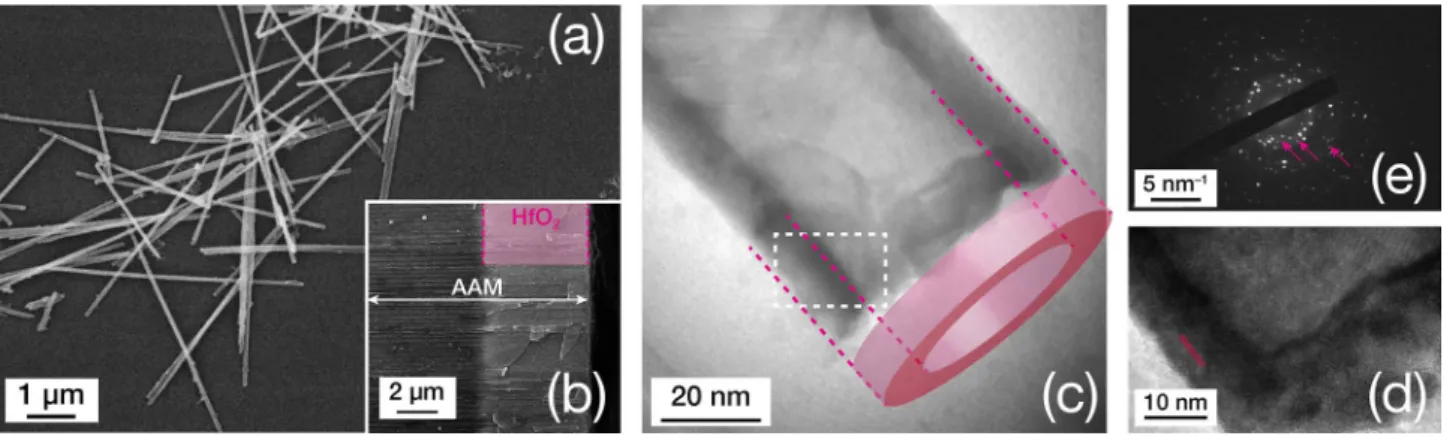
The morphology of the HfO2 layers has been observed by
SEM and TEM. Figure 3 shows the typical geometry of a film grown at T = 250◦C after N
HfO2 = 150 cycles. The
SEM images presented in Fig. 3a, b correspond, respec-tively, to the HfO2 deposit after the dissolution of the AAM
template in chromic acid and to a cross section of the sample after the ALD process. In both cases, they demonstrate that HfO2 is conformally grown on the walls of the nanoporous Al2O3. The brighter area located at the top surface of the
AAM (highlighted in pink on Fig. 3b) is ascribed to the HfO2 deposit. It indicates that the ALD of HfO2 proceeds homogeneously until a depth of 5.5 𝜇m. This is assessed by the nanotubes observed in Fig. 3a after the AAM removal that exhibit a longest length in the same range. The aspect ratio of such deposit is quite high (1:110) as compared to the best values (≈ 1:40) reported in the literature for this material [27, 32]. In addition, this ratio is compatible with
Fig. 2 a SEM top view of AAM grown in 0.3 M H2C2O4 at 40 V. b
High magnification view
Fig. 3 a SEM top view of HfO2 nanotubes after AAM dissolution
in chromic acid. b SEM cross section of an AAM template after the
ALD of HfO2. TEM image of a HfO2 nanotube grown at T = 250◦C
(NHfO2= 150cycles). The tubular geometry is highlighted by the pink
overlay. d High magnification view of the area located in the white rectangle drawn on c. e SAED corresponding to the area shown in d
the conformal deposition of conductive TiN films grown by thermal or plasma-enhanced ALD in similar AAM templates exhibiting aspect ratios of 1:125 and 1:75, respectively [25]. The free-standing nanotubes observed on Fig. 3a illustrate the mechanical integrity and stability of the HfO2 deposit.
The TEM analysis of the HfO2 nanotubes provides
addi-tional valuable information on the morphology and crystal-line structure of the deposit. Figure 3c presents a detailed view of a single HfO2 nanotube, where the cylindrical
geometry is highlighted by the pink ring drawn over the micrograph. The outer diameter is approximately 50 nm. It is equivalent to the pore opening of the AAM. The thickness of the tube walls, around 8 nm, is regular and homogeneous. This corresponds to a GPC of 0.5 Å/cycle. This value is similar to the GPC measured on planar surfaces (see below Fig. 7b) but slightly lower than other works in which a GPC of 0.8–0.9 Å/cycle is observed with the same precursors and temperature [32, 37–39]. As expected, the ALD process is well-suited for step coverage, since no HfO2 overhang is
observed at the tube mouth. Figure 3d shows a high magnifi-cation view of the area corresponding to the rectangle drawn in Fig. 3c. On this picture, the HfO2 atomic rows
correspond-ing to the (110) or (011) planes can be distcorrespond-inguished (they are highlighted by three pink lines). Together with the SAED shown in Fig. 3e, it indicates that the film grown at 250◦C is
crystalline. Although spots are visible on Fig. 3e, the HfO2
layer is polycrystalline, because various orientations are observed on the high magnification view shown in Fig. 3d and shaded rings corresponding to the (011), (− 111), and (− 202) planes can be seen on the SAED (see the arrows on the figure). Those rings are not sharp, because the probed area is not sufficiently large as compared to the size of the crystalline domains. As a consequence, the collected signal does not arise from numerous crystallites with various ori-entations and numerous spots are detected instead of rings. The XRD diffractograms presented in Fig. 4 show the crystalline structure of the bare AAM and after the ALD of HfO2 performed at 150 and 250◦C (N
HfO2 = 1000 cycles).
Before the HfO2 deposition two sharp peaks attributed to the
Al (200) and (220) planes are observed at 44.8◦ and 65.2◦,
respectively (PDF file 00-04-0787). The Al signal corre-sponds to the foil on which the AAM has been grown. A broad peak is also visible from 18 to 40◦ with a maximum
around 25◦. It corresponds to the amorphous alumina. After
the ALD of HfO2 at T = 150◦C, the Al (200) peak remains
unchanged, while the Al (220) diffraction is hidden by the hafnia layer. The broad peak ascribed to the amorphous AAM is modified after the ALD process. It is significantly narrower and centered around 32◦. This modification
corre-sponds to the amorphous HfO2 thin film grown on the AAM
template. It indicates that the ALD layer is not crystalline at this temperature. At T = 250◦C, the diffractogram exhibits
the same features, but small sharp peaks are clearly visible.
The comparison with the monoclinic HfO2 reference (PDF
file 00-34-0104) indicates that the ALD thin film is, at this temperature, crystallized. This is in agreement with the elec-tron diffraction pattern, as shown in Fig. 3e. These results indicate, therefore, that the films grown at low temperature (T = 150◦C) are mainly amorphous, while those formed at
higher temperature (T = 250◦C) are polycrystalline.
The chemical compositions of the HfO2 layers have been
analyzed by XPS. In both cases, hafnium, oxygen, and car-bon are detected on the as-grown layers. After a slight sur-face cleaning by Ar+ sputtering, the Hf and O signals remain
unchanged, while the C 1s peak disappears. It indicates that the carbon corresponds to a superficial contamination and not to an incorporation of the precursor ligands into the oxide films. Figure 5 presents the Hf 4f and O 1s peaks for the layers grown at T = 150 and 250◦C. The film
composi-tions do not depend on the deposition temperature, since XPS signatures are similar. On both Fig. 5a, b, the typical Hf 4f core levels are observed. The peaks are decomposed with the two contributions Hf 4f5∕2 and Hf 4f7∕2 centered at
17.9 and 16.2 eV, respectively. This is in line with the Hf4+
signature reported in literature for HfO2 [40–42]. The O 1s
peaks are shown in Fig. 5c, d. Although an FWHM slightly larger in Fig. 5d, the XPS signals are also very similar. In both cases, two contributions are observed. The main band, at low energy (E = 530.1 eV), is attributed to the oxygen of the HfO2 compound, while the component located at high
energy (E = 531.6 eV) can be assigned to the –OH species that likely arose from the use of water as second precursor. These analyses indicate, therefore, that the films grown at both temperatures have the same composition and corre-spond to HfO2.
20
Intensity (a. u.)
2 (deg) T = 150°C T = 250°C HfO2 reference AAM (a) (b) (c) 30 40 50 60 (100) (011) (110) (-111) (111) (002) (200) (220) (020) (200) (021) (022) (202) (220) (-122) (013) (131) (-302) (-213)
Fig. 4 X-ray diffractograms of the AAM with indexed Al planes (a)
and after ALD of HfO2 at 150◦C (b) and 250◦C with the monoclinic
HfO2 indexed planes (c). Green marks indicate the expected peaks for
To investigate the electrical properties of the HfO2 thin
films, current–voltage curves have been measured. The leak-age current as a function of the applied voltleak-age ranging from −5 to +5 V is plotted in Fig. 6. The current density meas-ured on the amorphous HfO2 film exhibits a lower value
(2 × 10⁻⁵
A ⋅ cm−2 at +5 V) as compared to the polycrys-talline one (2.5 × 10⁻⁴A ⋅ cm−2 at +5 V). These values are
larger than the currents reported in the previous studies for HfO2 films synthesized at temperatures higher than 250◦C
(up to 700◦C) [38, 39, 42]. In the literature, the crystalline
layers exhibit better dielectric properties than amorphous films. In the present case, the leakage current is higher for the crystalline films (i. e., one decade higher than the poly-crystalline one). These values are in a good agreement with HfO2 films grown at temperatures as low as 150◦C [43].
The leakage current measured for the crystalline films could be due to the presence of grain boundaries which are not present in the amorphous layer [44–46]. In the case of films grown at high temperature (up to 700◦C), one can assume
that the layers have a better crystallinity, i. e., the domains are larger, and thus, the density of grain boundaries is much smaller. The leakage current is, therefore, lower. The present results are, however, very encouraging and ALD appears as an appropriate method to provide homogeneous coatings even at low temperature (T < 150◦C) [33, 42].
The leakage currents presented on Fig. 6 are not sym-metric. This variation is ascribed to the use of two different metal contacts (Al and Au) on the probed layers. The respec-tive working functions of these materials are strongly differ-ent yielding a passivating native alumina layer that could be formed at the interface Al∕HfO2. It has to be noted that no
breakdown was observed for potentials as high as 5 V for a HfO2 thickness of 40 nm (it corresponds to an electric field of approximately 1.2 MV ⋅ cm−1).
The ultimate goal of this study was the fabrication of a TiN∕HfO2∕TiN 3D MIM system using a template-assisted ALD process. We reported previously the conformal dep-osition of TiN layers on AAM exhibiting aspect ratios as high as 1:125 and 1:75 using thermal and plasma-enhanced ALD, respectively [25]. Thus, successive ALD of TiN, HfO2, and TiN have been performed within the AAM as proof-of-concept of 3D-nanocapacitors. Figure 7 shows TEM micrographs of the resulting TiN∕HfO2∕TiN
stack-ing. Similar TiN∕HfO2∕TiN films were deposited on planar
silicon substrates (Fig. 7b) to facilitate the characterizations and provide to the experimentalist a larger range of use of thicknesses for each layer, without being constrained by the pore aperture. The TEM image of Fig. 7a demonstrates clearly that the deposition of the three layers is highly con-formal. As shown in Fig. 7b, the films are homogenous and the interfaces in between are sharp and well defined. It has to be noted that the top TiN layer was not modified or altered by the presence of the underneath HfO2 layer (crystalline in
the present case).
4 Conclusions
The ALD of HfO2 thin layers from TEMAHf and H2O has
been performed at 150 and 250◦C. It is shown that the
com-position remains unchanged, while the structure switches from amorphous to polycrystalline monoclinic HfO2 when
14 15 16 17 18 19 20
Counts (a. u.)
Counts (a. u.)
Hf 4f5/2 Hf 4f7/2 T=150°C Hf 4f T =250°C Hf 4f 14 15 16 17 18 19 20 Hf 4f5/2 Hf 4f7/2 (a) 528 529 530 531 532 533 534
Binding Energy (eV) 528 529 530 531 532 533 534
Binding Energy (eV)
T=150°C O 1s (c) OH OH T=250°C O 1s (d) (b)
Fig. 5 Comparison of the XPS peaks of HfO2 layers grown at 150
and 250◦C. Hf 4f peaks are shown in a and b and O 1s peaks are
shown on c and d. The temperatures of the ALD processes are indi-cated on the plots
-5 -4 -3 -2 -1 0 1 2 3 4 5 Voltage(V) 10-8 10-7 10-6 10-5 10-4 10-3 10-2 Current density (A cm –2) T = 150°C T = 250°C Si HfO2 Au Al
Fig. 6 j vs. U curves for pour HfO2 layers grown at T = 150 and
250◦C. The scheme drawn on the plot depicts how the electrical
measurements are performed: the back contact is established by the Al underlayer and the top contact by the Au dots
the process temperature is increased. This structural dif-ference has an impact on the electric properties, since the HfO2 film grown at low temperature exhibits better dielectric properties. This effect can be ascribed to the presence of grain boundaries in the polycrystalline oxide. Finally, the proof-of-concept of TiN∕HfO2∕TiN 3D-nanocapacitors is
demonstrated. At this stage, further electrical measurements should be performed on such systems to fully demonstrate the interest of the 3D architecture for production devices.
Acknowledgements The authors acknowledge D. Chaudanson and S. Nitsche for their precious help with the electron microscopy, V. Heres-anu for XRD measurements and interpretation, and S. Lavandier for the electrical measurements. This work was supported by the European Regional Development Fund (ERDF), the PACA Regional Council, the French Ministry of Higher Education and Research, and the CNRS.
References
1. G.D. Wilk, R.M. Wallace, J.M. Anthony, J. Appl. Phys. 89, 5243 (2001)
2. M. Gutsche. Memory cell with a stacked capacitor (2001). US Patent 6,207,524
3. A. Callegari, E. Cartier, M. Gribelyuk, H.F. Okorn-Schmidt, T. Zabel, J. Appl. Phys. 90(12), 6466 (2001)
4. M. Toledano-Luque, E. San Andrés, A. del Prado, I. Mártil, M.L. Lucía, G. González-Díaz, F.L. Martínez, W. Bohne, J. Röhrich, E. Strub, J. Appl. Phys. 102(4), 044106 (2007)
5. C.T. Tsai, T.C. Chang, P.T. Liu, P.Y. Yang, Y.C. Kuo, K.T. Kin, P.L. Chang, F.S. Huang, Appl. Phys. Lett. 91, 012109 (2007) 6. R.C. Smith, T. Ma, N. Hoilien, L.Y. Tsung, M.J. Bevan, L.
Colombo, J. Roberts, S.A. Campbell, W.L. Gladfelter, Adv. Mater. Opt. Electron. 10, 105 (2000)
7. J. Aarik, A. Aidla, H. Mändar, V. Sammelselg, T. Uustare, J. Cryst. Growth 220, 105 (2000)
8. S.M. George, Chem. Rev. 110, 111 (2010)
9. J.W. Elam, D. Routkevitch, P.P. Mardilovich, S.M. George, Chem. Mater. 15, 3507 (2003)
10. M. Putkonen, T. Aaltonen, M. Alnes, T. Sajavaara, O. Nilsen, H. Fjellvag, J. Mater. Chem. 19, 8767 (2009)
11. Y. Wu, L. Assaud, C. Kryschi, B. Capon, C. Detavernier, L. San-tinacci, J. Bachmann, J. Mater. Chem. A 3, 5971 (2015) 12. M.K.S. Barr, L. Assaud, N. Brazeau, M. Hanbücken, S. Ntais,
L. Santinacci, E.A. Baranova, J. Phys. Chem. C 121(33), 17727 (2017)
13. M.G. Willinger, G. Neri, E. Rauwel, A. Bonavita, G. Micali, N. Pinna, Nano Lett. 8, 4201 (2008)
14. K. Pitzschel, J. Bachmann, J.M. Montero-Moreno, J. Escrig, D. Goerlitz, K. Nielsch, Nanotechnology 23, 495718 (2012) 15. P. Banerjee, I. Perez, L. Lecordier-Henn, S.B. Lee, G.W. Rubloff,
Nat. Nanotechnol. 4, 292 (2009)
16. L.C. Haspert, S.B. Lee, G.W. Rubloff, ACS Nano 6, 3528 (2012) 17. K.B. Shelimov, D.N. Davydov, M. Moskovits, Appl. Phys. Lett.
77, 1722 (2000)
18. F. Roozeboom, R. Elfrink, J.F. Verhoeven, J. van den Meerakker, F. Holthuysen, Microelectron. Eng. 53, 581 (2000)
19. Sw Chang, J. Oh, S.T. Boles, C.V. Thompson, Appl. Phys. Lett. 96, 153108 (2010)
20. L.J. Li, B. Zhu, S.J. Ding, H.L. Lu, Q.Q. Sun, A. Jiang, D. Zhang, C. Zhu, Nanoscale Res. Lett. 7, 1 (2012)
21. K. M., M. Ritala, M. Leskelä, O.W. E, J. Carstensen, H. Föll, Microelectron. Eng. 84, 313 (2007)
22. J.H. Klootwijk, K.B. Jinesh, D. W, J.F. Verhoeven, F.C. Van Den Heuvel, H.D. Kim, D. Blin, M.A. Verheijen, R.G.R. Weemaes, M. Kaiser, J.J.M. Ruigrok, F. Roozeboom, IEEE Elec-tron. Dev. Lett. 29, 740 (2008)
23. T. Bertaud, C. Bermond, T. Lacrevaz, C. Vallée, Y. Morand, B. Fléchet, A. Farcy, M. Gros-Jean, S. Blonkowski, Microelectron. Eng. 87(3), 301 (2010)
24. Y. Matveyev, K. Egorov, A. Markeev, A. Zenkevich, J. Appl. Phys. 117, 044901 (2015)
25. L. Assaud, K. Pitzschel, M. Hanbücken, L. Santinacci, ECS J. Solid State Sci. Technol. 3, P253 (2014)
26. V. Miikkulainen, M. Leskela, R. Ritala, R.L. Puurunen, J. Appl. Phys. 113, 021301 (2013)
27. R.G. Gordon, D. Hausmann, E. Kim, J. Shepard, Chem. Vap. Depos. 9, 73 (2003)
28. I. Perez, E. Robertson, P. Banerjee, L. Henn-Lecordier, S.J. Son, S.B. Lee, G.W. Rubloff, Small 4, 1223 (2008)
29. D. Gu, H. Baumgart, G. Namkoong, T.M. Abdel-Fattah, Electro-chem. Solid-State Lett. 12(4), K25 (2009)
30. M.J. Choi, H.H. Park, D.S. Jeong, J.H. Kim, J.S. Kim, S.K. Kim, Appl. Surf. Sci. 301, 451 (2014)
31. J. Aarik, A. Aidla, A.A. Kiisler, T. Uustare, V. Sammelselg, Thin Solid Films 340, 110 (1999)
32. X. Liu, S. Ramanathan, A. Longdergan, A. Srivastava, E. Lee, T.E. Seidel, J.T. Barton, D. Pang, R.G. Gordon, J. Electrochem. Soc. 152(3), G213 (2005)
33. X. Fan, H. Liu, B. Zhong, C. Fei, X. Wang, Q. Wang, Appl. Phys. A 119, 957 (2015)
34. H. Masuda, K. Fukuda, Science 268, 1466 (1995)
35. E. Moyen, L. Santinacci, L. Masson, H. Sahaf, M. Macé, L. Assaud, M. Hanbücken, Int. J. Nanotechnol. 9, 246 (2012) 36. E. Moyen, L. Santinacci, L. Masson, W. Wulfhekel, M.
Han-bucken, Adv. Mater. 24(37), 5094 (2012). Kindly check and con-firm the edit made in author names in reference [36].
37. K. Kukli, M. Ritala, T. Sajavaara, J. Keinonen, M. Leskelä, Chem. Vap. Depos. 8, 199 (2002)
38. Y. Senzaki, S. Park, H. Chatham, L. Bartholomew, W. Nieveen, J. Vac. Sci. Technol. A 22, 1175 (2004)
39. P.D. Kirsch, M.A. Quevedo-Lopez, H.J. Li, Y. Senzaki, J.J. Peter-son, S.C. Song, S.A. Krishnan, N. Moumen, J. Barnett, G. Ber-suker, P.Y. Hung, B.H. Lee, T. Lafford, Q. Wang, D. Gay, J.G. Ekerdt, J. Appl. Phys. 99(2), 023508 (2006)
Fig. 7 a TEM micrograph of an MIM system (TiN/HfO2/TiN) grown
by ALD within an AAM (the template has been etched in chromic acid to allow the observation). The number of cycles is 50/100/50,
respectively. b TEM cross section of TiN/HfO2/TiN multilayers
40. C. Morant, L. Galán, J.M. Sanz, Surf. Interface Anal. 16(1–12), 304 (1990)
41. D. Barreca, A. Milanov, R.A. Fischer, A. Devi, E. Tondello, Surf. Sci. Spectra 14, 34–40 (2007)
42. A. Kumar, S. Mondal, K.S.R. Koteswara Rao, Appl. Phys. A 122, 1027 (2016)
43. K. Xu, A.P. Milanov, H. Parala, C. Wenger, C. Baristiran-Kaynak, K. Lakribssi, T. Toader, C. Bock, D. Rogalla, H.W. Becker, U. Kunze, A. Devi, Chem. Vap. Depos. 18(1–3), 27 (2012)
44. X. Zhao, D. Vanderbilt, Phys. Rev. B 65, 233106 (2002) 45. E.P. Gusev, C. Cabral Jr., M. Copel, C. D’Emic, M. Gribelyuk,
Microelectron. Eng. 69, 145 (2003)