Propriétés Optiques des Nanostructures d’Oxyde de Zinc (ZnO)
Texte intégral
Figure


Documents relatifs
Dans ce chapitre nous présentons et discutons les résultats obtenus dans les films préparés par la technique de spray ultrasonique, et nous avons étudies l'influence
chaque dopage.. Les valeurs de la bande interdite dans nos couches mince de ZnO se situent entre 3.20 et 3.33 eV. Elles sont en parfait accord avec les valeurs rapportées
Le présent travail consiste en l'élaboration et la caractérisation des couches minces de ZnO non dopées et dopées par différentes concentrations de cobalt (Co) (0.5, 1,
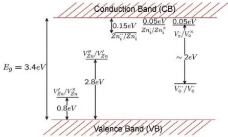
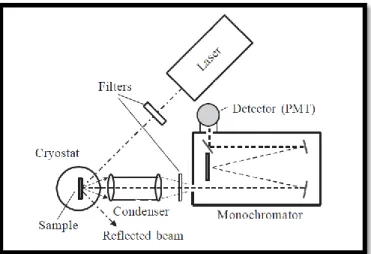
Les spectres de photoluminescence (PL) à basse température des couches minces de ZnO orienté plan-a obtenu par épitaxie sous jets moléculaire sur un substrat de
