Coherent Light-Matter Interactions
in Monolayer Transition-Metal Dichalcogenides
by
Edbert Jarvis Sie
B.S. Physics, Nanyang Technological University
Submitted to the Department of Physics
in partial fulfillment of the requirements for the degree of
Doctor of Philosophy
at the Massachusetts Institute of Technology
June 2017
C Massachusetts Institute of Technology 2017. All rights reserved.
Signature
A uthor...
redacted
Department of Physics May 24, 2017Signature redacted
Certified by...
_-.jV
Nuh Gedik
Associate Professor of Physics
Thesis Supervisor
Signature
Accepted by...
MASSACHUSETTS INSTITUTE OF TECHNOLOGYJUN 27 2017
LIBRARIES
ARCHIVES
redacted
Nergis Mavalvala
Professor of Physics
Associate Head, Department of Physics
Coherent Light-Matter Interactions
in Monolayer Transition-Metal Dichalcogenides
Edbert Jarvis Sie
Submitted to the Department of Physics on May 24, 2017, in partial fulfillment of the
requirements for the degree of Doctor of Philosophy
Abstract
Semiconductors that are thinned down to a few atomic layers can exhibit novel properties beyond those encountered in bulk forms. Transition-metal dichalcogenides (TMDs) such as
MoS2, WS2 and WSe2 are prime examples of such semiconductors. They appear in layered structure that can be reduced to a stable single layer where remarkable electronic properties can emerge. Monolayer TMDs have a pair of electronic valleys which have been proposed as a new way to carry information in next generation devices, called valleytronics. However, these valleys are normally locked in the same energy level, which limits their potential use for applications.
This dissertation presents the optical methods to split their energy levels by means of coherent light-matter interactions. Experiments were performed in a pump-probe technique using a transient absorption spectroscopy on MoS2 and WS2, and a newly developed XUV light source
for time and angle-resolved photoemission spectroscopy (TR-ARPES) on WSe2 and WTe2.
Hybridizing the electronic valleys with light allows us to optically tune their energy levels in a controllable valley-selective manner. In particular, by using off-resonance circularly polarized light at small detuning, we can tune the energy level of one valley through the optical Stark effect. At larger detuning, we observe a separate contribution from the so-called Bloch-Siegert effect, a delicate phenomenon that has eluded direct observation in solids. The two effects obey opposite selection rules, which enables us to separate the two effects at two different valleys.
Monolayer TMDs also possess strong Coulomb interaction that enhances many-body interactions between excitons, both bonding and non-bonding interactions. In the former, bound excitonic quasiparticles such as biexcitons play a unique role in coherent light-matter interactions where they couple the two valleys to induce opposite energy shifts. In the latter, non-bonding interactions between excitons are found to exhibit energy shifts that effectively mimics the Lennard-Jones interactions between atoms. Through these works, we demonstrate new methods to optically tune the energy levels of electronic valleys in monolayer TMDs.
Thesis Supervisor: Nuh Gedik Title: Associate Professor of Physics
Acknowledgments
First and foremost, I would like to thank my advisor Prof. Nuh Gedik for his mentorship and support. He has been a constant source of inspiration since I first started my graduate studies. Actually it was even before that. I remember my first meeting at a conference in Boston where he presented a real-time image of crystalline lattice motion. The idea of watching Michael Jackson performing Billie Jean flashed through my head, because he was that cool and inspiring, and he continues to be so. He has been a tremendous support since day one, where I was given the opportunity to design and build the XUV beamline for ARPES in the lab as well as the freedom to build the white-light setup next to it. His vigor to make new innovations in time-resolved experiments is always inspiring. Throughout my graduate studies, he has been a true role model of how to be a good scientist and to search for a good question like 'So what?' in a perfectly well stated manner. I also learn that "no problem is too small, and no problem is too
big". He gave me and other group members many opportunities to attend international conferences with the intention that we could learn how to communicate our findings with new
people and meet fellow scientists in the field. Despite his busy schedule, he always makes time to discuss with group members regularly through the weekly group meetings, bi-weekly sub-group meetings, and individual meetings. Apart from discussing about research, he has been a
constant source of encouragement and guidance where he would chat to discuss about our
personal matters and future careers. Sometimes I was left wondering how one person can do so much in a little time and can become so quick and sharp minded like laser while being gentle at
all times. I sincerely thank Nuh for every aspect of my graduate education.
I am very grateful to other members of my thesis committee, Prof. Liang Fu and Prof.
Pablo Jarillo-Herrero. Liang has been a theory advisor to me where many fundamental explanations of my experiments are inspired by him. One of many insightful wisdoms, he taught me that the optical Stark effect can be extended to create a topologically nontrivial phase of matter in monolayer TMDs. Discussing research with him has always been exciting and
stimulating, not because we know anything more about the theory, but because he knows very well the reality about what the experiments can do. Much of the theory I understand has been patiently explained to me after I went to his office several times. He showed me to use simple diagrams and mathematical expressions that capture the essence of physics. I will remember to use the Cartesian coordinates every time I face the spherical harmonics.
Pablo has been my academic advisor at MIT where he regularly checked up my academic progress throughout my graduate studies. His office is like the holy and respected temple where I can freely confess about my classes, research progress, academic career, and ask for his
guidance. I always remember his suggestions that a lot of times it is better to complete tasks one
at a time rather than attempting to complete everything at once. I sincerely thank Pablo for letting me have the access for his labs to borrow some optics or to perform sample
characterization with his group members. Every time I entered his fabrication lab, most likely to ask his group members out for lunch or dinner, I always feel humbled because this lab have very
highly skilled people who are capable of creating cool devices.
My learning and working experience in the lab has been very enjoyable because of the highly spirited colleagues in the Gediklab. I am very grateful to Yihua Wang (now professor at
Fudan) who has taught me the 'Introduction to Gediklab 101' since I first joined the group in August 2011. He constructed the ARPES system in the lab and taught me how it works and how to use it. I learned how to use Solidworks from him in order to accurately design and assemble many ultra high vacuum (UHV) apparatus for the new extreme ultraviolet (XUV) beamline in the lab. Since then it has becoming my favorite software to draw three-dimensional figures, some of them appears in the last chapter of this dissertation. David Hsieh (now professor at Caltech) has always been inspiring and he introduced me to many interesting material systems that can be explored. Timm Rohwer has been a great colleague that I had a real pleasure to work together with and a good friend to have. He joined the group during my third year and since then we have been working together to setup the XUV beamline for ARPES. He has an infinite reservoir of energy and motivation, which constantly inspires me. There is no lab equipment that he cannot fix. Zhanybek Alpichshev has been a constant source of joy and inspiration in the office. I am very fortunate to share an office with him. I learn something new almost every time I had conversation with him. There is no question that he cannot answer. Joshua Lui (now professor at
UC Riverside) taught me how to write stories clearly and worth telling. He gave me very helpful
advices during my transition from a graduate student into a more devoted profession in later stage of my career.
I also enjoyed having discussions with former group members James McIver, Alex
Frenzel, Darius Torchinsky, Daniel Pilon, Fahad Mahmood, Byron Freelon, Inna Vishik, Hengyun Zhou, Mahmoud Ghulman, and Steven Drapcho. As well as with current group members Ozge Ozel, Changmin Lee, Emre Ergecen, Alfred Zong, Anshul Kogar, Carina Belvin, Suyang Xu, Nikesh Koirala, Mehmet Yilmaz, Guy Marcus, and Edoardo Baldini. They are very talented individuals and enjoyable to work with in the lab. There were many good memories that we shared together which enriched my experience as a graduate student at MIT.
Outside our lab, I am very thankful to Prof. Yi-Hsien Lee (now professor at NTHU Taiwan) and Prof. Jing Kong for their expertise and generous supports to synthesize the high-quality monolayer TMDs that I used in all of my experiments. My first encounter with Yi-Hsien in the corridor of MIT Building 13 results in a long-lasting friendship and professional collaboration, which I look forward to continue in future. I would like to thank Wenjing Fang, who happens to be the source of all interesting information surrounding our community. I remember her telling me about the new thin semiconducting materials that could be synthesized in Jing's group with the help from Yi-Hsien. This started my pursuit in studying the monolayer TMDs. I am very grateful to my wonderful friend and colleague Qiong Ma from Pablo's group for being my study buddy over the years. She shows a great and professional enthusiasm at work
(and outside...), which inspires me to work harder and be more productive. Every time I have questions regarding graphene or low-dimensional devices, she has always been the first person I had to consult with, and she usually gave more useful tips beyond my questions. She is like a living dictionary made of graphene; ... I mean a strong one that can even hold an elephant!
Everybody knows this is not a joke, right. I also thank Yaqing Bie and Yuan Cao for being my dinner buddies whenever I have a craving for good foods (like every time...). Yaqing, the 'Queen of Optics' in Pablo's group, has always been helpful every time I wanted to discuss about optics in low-dimensional devices. I also thank the rest of the people in MIT Building 13: Yafang Yang, Linda Ye, Shengxi Huang, Yuxuan Lin, Lin Zhou, and Xi Ling (now professor at Boston University) who have been amusing companions during my graduate studies, as well as in exploring different options for oriental foods. I thank Raga Markely for being my lunch buddy where I can also share my thoughts about everyday life and future career. I am very grateful to Monica Wolf who has done a lot more than being our admin secretary. She took care everything about travel plans, reimbursements, lab equipment purchases, employment transition, as well as the big celebration for thesis defense (with the help from Qiong and Ozge) that I went through, multiplied by the number of people like me in MIT Building 13, floor 2.
I would like to thank Christopher Gies and Alexander Steinhoff in University of Bremen, Germany for their immense contributions in the theoretical study of highly excited monolayer TMDs, presented in Chapter 7. It was a wonderful experience to collaborate with Chris and Alex, from whom I learned a great deal about the role of plasma screening in monolayer TMDs.
Throughout the years as a graduate student, there are also other researchers whom I often encountered at conferences: Jonghwan Kim, Long Ju, Xiaoxiao Zhang, Yilei Li, Ziliang Ye, Jan Buss, and Shiang Fang. I am very grateful to know them, which makes the conference visit more interesting and more fruitful, because we work in a similar field and we can learn from each other. I am sure I will see them more often in future, and I look forward to it.
My very special gratitude goes to my parents for their unconditional love, support and
wisdom. My mother taught me how to speak, to stand, and to love one another. My father fixed what my mother taught me.
Edbert J. Sie Cambridge, MA
Table of Contents
1. Introduction
11Mr A.. Mnrm mtal dich1 dirhnJLn Pi nides (TMn fIm )..
1.1.1. Electronic bandstructure
1.1.2. Optical selection rules...
1.1.3. Excitons ...
1.2. Time-resolved spectroscopy... 1.2.1. Coherent light-matter interactions 1.2.2. Quasi-equilibrium dynamics ...
2. Time-resolved absorption spectroscopy
2.1. Experimental setup ... 2.1.1. Overview ...
2.1.2. Laser am plifier ...
2.1.3. Optical parametric amplifier ...
2.1.4. White light continuum ... 2.2. Data analysis...
2.2.1. Kramers-Kronig analysis... 2.2.2. Maxwell's equations for monolayer
3. Intervalley biexcitons in monolayer MoS2 3.1. Intervalley biexcitons ... 3.2. Experimental methods ...
samples.
3.3. Experimental results & discussion ... 3.3.1. Intravalley & intervalley scattering. 3.3.2. Signature of intervalley biexcitons .
3.3.3. Time-resolved cooling process ....
3.4. Conclusions...
4. Valley-selective optical Stark effect in monolayer WS2
4.1. Optical Stark effect... 4.1.1. Sem i-classical description ...
4.1.2. Quantum-mechanical description... 4.2. Experim ental m ethods ...
4.3. Observation of the optical Stark effect ... 4.4. Valley-selectivity ...
4.5. Fluence & detuning dependences ...
4.6. Proposal: valley-specific Floquet topological phase in TMDs ... 66
Page 9 of 164 S. ... . ... . ... . ... .. ... ... ... ... ... ... . . . . . . . . . . . . ... ... ... . . . . 13 15 15 18 21 22 23 24 25 26 26 28 29 31 34 35 37 41 42 44 45 46 47 48 50 53 54 55 59 60 60 63 65
4.7. Supplem entary ...
4.7.1. Tim e-resolved spectra ... 4.7.2. Polarization-resolved spectra ... 4.7.3. Obtaining the energy shift ... 4.7.4. Comparison from semi-classical theory ...
5. Intervalley biexcitonic optical Stark effect in monolayer WS2
5.1. Blue detuned optical Stark effect ...
5.2. Experim ental m ethods ...
5.3. Experimental results & data analysis ...
5.4. Intervalley biexcitonic optical Stark effect ... 5.4.1. Four-level Jaynes-Cummings model ... 5.5. Perspective: Zeeman-type optical Stark effect ...
5.6. Supplem entary ...
5.6.1. Coherent & incoherent optical signals ... 5.6.2. Time-trace fitting decomposition analysis ... 5.6.3. Possible effects under red-detuned pumping ...
5.6.4. Fitting analysis ...
6. Large, valley-exclusive Bloch-Siegert shift in monolayer WS2
6.1. Bloch-Siegert shift ... ... 6.1.1. Sem i-classical description ...
6.1.2. Quantum-mechanical description ... 6.2. Experim ental m ethods ...
6.3. Observation of the Bloch-Siegert shift ...
6.4. Fluence & detuning dependences ...
6.5. Valley-exclusive Optical Stark shift & Bloch-Siegert shift ... 6.6. Conclusions ...
7. Lennard-Jones-like potential of 2D excitons in monolayer WS2 7.1. Many-body interactions in 2D TMDs ...
7.2. Experim ental m ethods ...
7.3. Optical signature of many-body effects ... 7.3.1. Exciton redshift-blueshift crossover ... 7.3.2. At low density: plasma contribution ... 7.3.3. At high density: exciton contribution ...
7.4. Lennard-Jones-like potential as an effective model ...
7.5. Chronological signature of interactions in time-resolved spectra. 7.6. Sum m ary ... 7.7. Supplem entary ... 68 68 70 71 73 75 76 77 78 82 83 86 86 86 89 92 92 95 96 98 101 104 104 107 108 111 113 114 115 117 117 119 120 121 123 126 126
7.7.1. Microscopic many-body computation... 126
7.7.2. Exciton-exciton annihilation effect ... 130
7.7.3. Heat capacity and estimated temperature ... 131
8. XUV based Time-resolved ARPES 137 8.1. Building a high-resolution Extreme UV light source for TR-ARPES ... 138
8.1.1. Overview ... 138
8.1.2. XUV light source ... 140
8.1.3. XUV m onochrom ator ... 143
8.1.4. XUV diagnostic chamber ... 146
8.2. Measuring TMDs using 30 eV XUV TR-ARPES ... 148
8.2.1. W Se2 sem iconductor... 148
8.2.2. W Te2 semimetal ... 151
References 155
Chapter 1
Introduction
Contents
1.1. Monolayer transition metal dichalcogenides (TMDs) 1.1.1. Electronic bandstructure
1.1.2. Optical selection rules
1.1.3. Excitons
1.2. Time-resolved spectroscopy
1.2.1. Coherent light-matter interactions 1.2.2. Quasi-equilibrium dynamics
Page 13 of 164
k
Two-dimensional materials can exhibit novel properties beyond those normally encountered in the bulk compounds. Most evidently is the change in their electronic density of states and their increasing susceptibility to a Peierls transition. More interestingly, a number of fascinating phenomena emerge from two-dimensional materials. This includes quantum well system with quantized energy levels, two-dimensional electron gas (2DEG) that can exhibit the integer and fractional quantum Hall effect, layered materials that demonstrate high-temperature superconductors, as well as topological insulators that feature nontrivial metallic states at the surface while remain insulating on the inside. Some of these material systems can appear as compounds from multiple different elements with complex lattice structures while maintaining their quasi two-dimensionality.
Graphene, a single layer of carbon atoms, is a prime example of such 2D materials that can exhibit some of the above remarkable properties despite its very simple structure. The electronic structure of graphene is described by a massless Dirac fermion at around the Fermi level, with the valence and conduction bands touching at a single point [7]. This allows graphene to exhibit extremely high electron mobility, which is a promising property in developing nanoscale electronic applications. However, the gapless electronic structure in graphene makes it challenging to use this material for switchable electronics such as transistors. Various approaches can be used to open a gap in graphene [8], for example by placing graphene above a particular substrate that breaks graphene's sublattice symmetry. However, the resulting gap induced this way is reported to be around 100 meV [9], which is still rather small for practical applications.
Transition-metal dichalcogenides (TMDs) comprise a family of II-VI semiconductors
such as MoS2, WS2, MoSe2 and WSe2. These materials are layered in structure, from which
we can isolate a monolayer of TMDs through mechanical exfoliation or chemical vapor deposition (CVD) growth method [10, 11]. Monolayer TMDs have a lattice structure similar to graphene but, unlike graphene, these materials possess a semiconducting gap between 1-2 eV. The large gap in this class of materials offers promising electronic applications based on two-dimensional materials. Recently, a microprocessor based on a 2D semiconductor (MoS2) has been reported [12]. The device consists of 115 transistors
(a) (b)
S ---- :::--- M o
Mo
SS
Figure 1.1: (a) Unit cell of monolayer 2H-MoS2 in a trigonal prismatic arrangement. This
structure lacks an inversion center. (b) Top view of monolayer 2H-MoS2.
comprising all basic building blocks that are common to most microprocessors. While this class of materials could be an important element for the development of future 2D devices, they are found to have novel electronic and optical properties as we discuss below.
1.1. Monolayer transition-metal dichalcogenides (TMDs)
The properties of monolayer TMDs were first studied through pioneering optical measurements on monolayer MoS2 by Mak et al. [13] and Splendiani et al. [14]. Monolayer MoS2 is a one-unit-cell thick semiconductor with a graphene-like hexagonal lattice of Mo and S atoms where the S-Mo-S layers are stacked in a trigonal prismatic arrangement (Fig
1.la-b). It is a direct band gap semiconductor with an optical energy gap of 1.96 eV (10 K)
at K and K' valleys in the Brillouin zone and a valence band splitting of 160 meV due to strong spin-orbit coupling (Fig 1.2). Other monolayer TMDs have similar properties but the magnitudes differ slightly, for example monolayer WS2 has an optical gap of 2.1 eV at
300 K and a valence band splitting of 400 meV. Monolayer TMDs are promising material
systems for future low-energy electronics because it has a unique spin-valley coupling and a strong Coulomb interaction.
1.1.1. Electronic bandstructure
In this section we describe the electronic bandstructure of monolayer MoS2, following the theoretical studies by Xiao et al. [15] and Liu et al. [2, 16], but the general
Page 15 of 164
_AMM
K
K1
CB K'
K K
VBK
Figure 1.2: Hexagonal Brillouin zone of monolayer MoS2. The band edges from conduction
bands (CB) and valence bands (VB) are located at the K and K' points.
description should also applies to WS2, WSe2, and MoSe2 monolayers. The bandstructure of monolayer MOS2 around the gap is well described by considering the Mo-d orbitals and S-p
orbitals. This material has a unit cell that forms a trigonal prismatic coordination around
the Mo atom that splits its d orbitals into three groups: A1 (dz2), E(dxy, dX2_y2) and
E'(dxz, dyz). The mirror symmetry along the 2 direction allows a hybridization between A1
and E orbitals, which constitutes the gap opening at the K and K' valleys in the Brillouin zone (Fig 1.3). In the vicinity of these symmetry points, the wavefunction of the bands are
described by the following symmetry-adapted basis functions:
1
kpc) = Idz2),
140
= -(I|dX2Y2) i idxy)) (1.1)where 10c) is the basis for conduction band, lP5,) for valence band, and the + sign denotes
the K or K' valley index. The two-band Hamiltonian of monolayer MoS2 mimics that of
graphene because both systems have similar symmetry properties, except for the gap
opening due to the differing on-site potentials between the Mo and S sublattices and the
strong spin-orbit coupling (SOC) originated from the Mo-d orbitals:
A-1
(2)
H = at( kx + ky y)+sz - l " 2 T A (1.2)
5
4 a) ( a )y( b ) ( C )
-4
F K M F K M F K M 1?
Figure 1.3: Atomic orbital projection of band structures for monolayer MoS2 from first-principle
calculations, without spin-orbit coupling. Fermi energy is set to zero. Symbol size is proportional to its contribution to corresponding state. (a) Contributions from Mo-d orbital. (b) Total contributions from p orbitals, dominated by S atoms. (c) Total s orbitals. Figure is obtained from Reference [2].
where a is the lattice constant, t the hopping integral, k the wavevector, 68 the Pauli matrices for the two basis functions, A the energy gap, 22Z the spin splitting at the top of the valence band caused by the SOC interaction H' = .L S (i = 2,m5 = 1/2), and sz the
Pauli matrices for the electron's spin.
There are three important features that distinguish monolayer MoS2 from graphene.
First, the resulting electronic structure is described by a massive Dirac fermion due to the
finite gap in the second term. This allows an interband electronic transition at the K and K' valleys that can be induced through an optical excitation in the visible regime. Second, the two valleys possess finite and opposite Berry curvatures owing to the lack of crystalline inversion symmetry. This gives rise to distinct optical selection rules, which we will discuss further in the next section. Third, the SOC contribution in the third term leads to a large spin splitting at the valence band top (160 meXT). Meanwhile, the spin splitting at the conduction band bottom is negligible in the first-order approximation because it is mostly
K K'
= +1
2
Figure 1.4: Optical selection rules in monolayer MoS2.
composed by dz orbital (i = 0). Its magnitude can be obtained by using a second-order perturbation from the Mo-d orbitals and a first-order perturbation from the minor S-p
orbitals (i 1 = 1) [4]. Although the conduction band splitting is much smaller in
magnitude (3 meV in MoS2), it plays an important role in the formation of stable dark excitons in monolayer WS2 and WSe2 [17] where the splitting is larger (20-40 meV) and inverted.
1.1.2. Optical selection rules
In monolayer TMDs, the two valleys couple differently with left and right circularly polarized light [15, 18-2 0]. At K valley, optical transition from the valence band top (VB) to the conduction band bottom (CB) is induced exclusively by left-circularly polarized light. At K' valley, the optical transition is induced exclusively by right-circularly polarized light. Such valley selection rules arise from the different quantum numbers in associated to the
bands at the two valleys (Fig 1.4). At K valley, the valence bands are assigned in = -1/2 and
+1/2
for the down-spin and up-spin respectively, while the conduction bands areassigned mn = -3/2 and -1/2 for the down-spin and up-spin respectively. Interband
transitions from VB to CB can occur through absorption of left-circularly polarized light
(r-)
that carries an angular momentum Am = -1, where we consider electric dipoleapproximation that leaves the spin unchanged. At K' valley, the quantum numbers have the opposite signs with respect to the K valley because of time-reversal symmetry. Hence,
interband transition at K' valley can occur through absorption of right-circularly polarized light (u-) with Am = +1.
The above description can explain the origin of valley selection rules because the quantum numbers are given. However, obtaining these quantum numbers is not as straightforward as the addition of orbital and spin angular momenta in atoms. Isolated atoms in free space have a full spherical symmetry that allows electron orbitals to acquire magnetic quantum numbers m = 0, 1, 2,i3,.... with no limit. Meanwhile, the crystal
lattice of monolayer TMDs has a space group D3h that imposes a trigonal symmetry C3 at
the K symmetry points, so the linear combination of atomic orbitals (LCAO) throughout the
lattice must conform this symmetry. This limits the effective quantum numbers m =
0, 1, 2 (modulo 3) that can be present in the system.
In order to obtain the quantum numbers of the conduction and valence bands, we must find the eigenvalue Ya (a = c, v) of the C3 rotation on the Bloch functions C3 ', = Ya'Pa. This should include both the constructing atomic orbitals and the plane wave
component of the Bloch functions, expressed as
ia(r) = e iK-(r+)da(r - R - 6) (1.3)
R
where R is the lattice vector, 6 is the position of Mo atom in the unit cell, dc = dz2 and
dv = (d2 -y 2 idxy)/vZ. There are two contributions to the eigenvalue, first the C3
rotation about the center of atomic orbital C3dc = dc and C3d, = e i2n/3d., and second the change of lattice phase factor e iK.r at each lattice site. The eigenvalue Ya depends on the position of the rotation center p, which can be Mo atom, S atom or the h position (center of hexagon), as shown in Fig 1.5 (inset). By using symmetry analysis of C3 on the above Bloch
functions, we can obtain the eigenvalue
Ya = e iK-(C3 -)yda (1.4)
where 6 is the Mo atom position with respect to the rotation center p, and Yda is the
eigenvalue about the center of atomic orbitals [16]. In short, the orbital quantum number
p= Mo K K' -Ye =1 c=1 IN = es 3 , = e-' Tn, = 0 m, = 0 M51 = -i m., = +} mi = -} mj = +} m1=+} m1=-O M, +1 Tn,= -1 1n,= -2 n,
2=-p
= S I K K' 7c =e 3c e 3 7V = e- 3 y = e 3 CB VB Mo ph S p = h K K' 7/C = e 3 c I= e3 7Y. = I 7.V = 1 CB VB K 3 2 +1 3 -~t Am= -1 K' + 01+ (T+ t2 Am + 1Figure 1.5: The C3 rotation eigenvalues Yc,v [2] and quantum numbers of bands in monolayer
MoS2, specified for different rotation centers p = Mo, S, and h positions (see inset). The
quantum numbers inside the middle row are shown only for the band edges, i.e. spin-down at K valley and spin-up at K' valley.
m, is obtained from y = exp(i2wm1/3). The simplest example is given at p = Mo (6 = 0)
where the lattice phase contribution is zero and hence y" = ydc = 1 and y?1 = yd, =
e i21T/3. The conduction bands are assigned m, = 0 at K and K' valleys, while the valence
bands are assigned m, = -1 at K valley and +1 at K' valley. By adding the spin
contributions m, we can obtain the total quantum numbers m1 of these bands (Fig 1.5).
We emphasize that the quantum numbers associated with conduction and valence bands depend on the choice of rotation center, but the upward optical transition between
CB VB M = +1 Tn, -1 mj +} mj -i my=-~ i 18 2 mst=+jM' +12 3i i 3 M, = -1 Tn, =+1 m81 = -} 2 m 't = +} 2-mi = -i mj = +1 m=- 2 m=+}i= 1 +1 K K' 1 2 2 22 +7(7 2 2 3 3 t 2 Am-1 Am +1 K K' 2 2 2 4 Am = -1 m=+ 0~q+ 2 4 2~ 16 .q
the spin-conserving bands remain the same, i.e. Am = -1 at K valley and +1 at K' valley.
This is a consequence of the lattice symmetry in monolayer TMDs that also gives rise to the nonzero and opposite Berry curvatures at the K and K' valleys. Berry curvature can be viewed as the self-rotating motion of the electron wavepacket or the orbital magnetic moment, and the opposite Berry curvatures between the K and K' valleys give rise to the opposite selection rules at the two valleys.
1.1.3. Excitons
Upon photoexcitation, an electron will occupy the conduction band and leave a hole in the valence band. They have opposite charges and can attract each other through Coulomb interaction. This allows a formation of bound quasiparticle called an exciton. Monolayer TMDs are atomically thin semiconductors; so electronic excitation is confined within 2D structure similar to the situation in quantum wells. There are two important consequences that differentiate the excitons in this system and in the bulk. First, there is a strong spatial overlap between the electron and hole orbitals in the I direction due to quantum confinement. Second, the electric field between the electron-hole pair can penetrate outside the material where screening is absent (Fig 1.6a-c). These two features enhance the Coulomb attraction significantly and result in the large excitonic binding energy of 320 meV in monolayer TMD WS2 as compared to 50 meV in bulk WS2 [6]. The
binding energies are determined through comparing the series of exciton energy levels obtained experimentally and theoretically. Note that as the electron-hole separation increases, a larger amount of electric field between them penetrates outside the material and the overall screening gets suppressed. This leads to a pronounced deviation from the usual hydrogenic series of exciton energy levels.
The optical selection rules in previous section are discussed in terms of one-particle picture where Coulomb interaction between the electron-hole pair is ignored. Note that the selection rules result from the symmetry properties in monolayer TMDs. Since Coulomb interaction appears as 1/r with a full spherical symmetry, the symmetry properties in monolayer TMDs are unaffected. Thus, novel selection rules at the two valleys are
(a) Bulk (3D)
Exciton
!
0
-0
3D
Z A band gap
Photon energy
Figure 1.6: Interactions between electron and hole that form an exciton is mediated by Coulomb attraction. (a) In bulk, the electric field is screened by the surrounding material. (b) In monolayer, large fraction of the electric field penetrates outside the material into the vacuum where screening is absent, or to an appropriate substrate where screening can be varied. (c) The suppressed screening in monolayer leads to a larger exciton binding energy with respect to the band gap. Figures are adapted and redrawn from Reference [6].
maintained, and excitons can be created in a valley-selective manner using circularly polarized light.
1.2. Time-resolved spectroscopy
Monolayer TMDs have a pair of electronic valleys (K and K') whose index can be used as a new degree of freedom for next generation valleytronics. Owing to the optical selection rules, we can use left-circularly polarized light to promote charge carriers at K valley to carry information with valley index of -1. However, since the two valleys are energetically degenerate, these carriers can scatter from K valley to K' valley and carry the incorrect valley index of +1 (Fig 1.7). Such intervalley scattering introduces a valley index mixture throughout propagation until the population between the two valleys reaches equilibrium. In order to use the valley index for practical valleytronic devices, it is desirable to suppress the intervalley scattering. There are two methods to follow up on this line: (i) split the energy levels between the two valleys, and (ii) identify the dominant intervalley scattering mechanisms and suppress its scattering rate. In our approach, we use light-matter interactions in a time-resolved manner to achieve this.
Exciton
K K'
Figure 1.7: Intervalley scattering of charge carriers from K valley to K' valley.
1.2.1. Coherent light-matter interactions
Hybridizing light with electrons in materials can result in newly created photon-dressed states or Floquet states with energy levels that are modified from their original states. An effective hybridization can be achieved in materials that are subject to a coherent light field so there exists a phase correlation between the induced polarization and the incident light. Hence the resulting hybrid quasiparticle, when written using Bogoliubov transformation, can maintain well-defined amplitude and energy. This is in a similar situation with the forced harmonic oscillator, where the interaction energy is transferred periodically between light and electrons in materials without energy loss. In practice, energy loss can occur through incoherent interactions. This could be mediated by dissipative scattering channels upon absorption of resonance light.
In order to suppress the absorption process, we use coherent light source (laser) that is tuned resonance with the material system. Coherent interactions with off-resonance light can be used to shift the energy levels of materials. As we will discuss in later chapters, the energy shift (often called the "light shift") can occur through two mechanisms, the optical Stark shift and the Bloch-Siegert shift. These processes can be used to split the energy level between the two valleys using circularly polarized light that breaks time-reversal symmetry. This optical technique can offer a much larger energy splitting as compared to that of magnetic field.
1.2.2. Quasi-equilibrium dynamics
In monolayer TMDs, excitons can be created at a specific valley and switched to the other valley through intervalley scattering. The lifetime of this scattering process can be measured using pump-probe spectroscopy, which can occur in subpicosecond timescale. In this experiment, a left-circularly polarized pump pulse is used to create excitons at K valley and no excitation at K' valley. After some time delay, exciton populations at K and K' valleys are monitored using left- and right- circularly polarized probe pulse. The intervalley scattering process can be measured through the increasing bleaching signal at K' valley in time-resolved absorption spectroscopy or through the decreasing polarization rotation of the probe pulse in time-resolved Faraday or Kerr spectroscopy. The obtained scattering lifetime can be scrutinized through its dependencies in temperature, charge doping, spin-orbit coupling strength, exciton density, and substrates. As such, the dominant intervalley scattering mechanism can be identified and the scattering rate can be suppressed.
Mutual interactions between excitons can also be probed using time-resolved spectroscopy. In later chapters, we will discuss the bound state of two excitons, called biexciton, which can be induced using two-step excitation. Two excitons that are created at two different valleys can form an intervalley biexciton, which possess a unique combination of orbital, spin and valley degree of freedoms, with no analogue in atomic systems. Non-bonding interactions between two separate excitons can also occur through atom-like van der Waals interactions. Unlike atoms, however, excitons usually have much smaller binding energies and can break into free electron-hole pairs or plasma. This introduces
complexities to non-bonding interactions between excitons in conventional
semiconductors. Monolayer TMDs, on the other hand, provide a special platform for exploring quasiparticle interactions because of their unique two-dimensionality and strong Coulomb interactions, which render these quasiparticles stable at room temperature. This should allow more in depth studies of such interactions at higher excitation density regime that was previously unexplored in conventional semiconductors.
Chapter 2
Time-resolved absorption spectroscopy
Contents
2.1. Experimental setup
2.1.1. Overview 2.1.2. Laser amplifer
2.1.3. Optical parametric amplifier
2.1.4. White light continuum
2.2. Data analysis
2.2.1. Kramers-Kronig analysis
2.2.2. Maxwell's equations for monolayer sample
Page 25 of 164
This dissertation work emphasizes on the exciton energy shift that is induced by femtosecond light pulses. At equilibrium, the exciton energy level in monolayer TMDs sits in the visible regime, e.g. EO = 2 eV in monolayer WS2. In order to detect this energy shift,
we need a broadband probe pulse that is centered in the visible spectrum. White light continuum generation is a nonlinear optical process capable of producing such broadband light pulse between 500-700 nm (hw = 1.8 - 2.4 eV). In this chapter, we will discuss about time-resolved absorption spectroscopy setup (or simply transient absorption) that utilizes white light continuum to probe the exciton energy shift in monolayer TMDs. In the first section, we will show the overview of the transient absorption setup. In later sections, we will discuss in more details about (i) laser amplifier, (ii) optical parametric amplifier, and (iii) white light continuum generation. Finally, we will discuss about the data analysis based on the optical physics of monolayer materials on a transparent substrate.
2.1. Experimental setup
2.1.1. Overview
Transient absorption spectroscopy consists of synchronized pump pulses and broadband probe pulses to monitor the pump-induced absorption of materials. Light has three properties namely photon energy, polarization and intensity that, when tuned precisely, can induce various nonequilibrium phenomena in materials. Examples are resonant excitation of quasiparticles, off-resonance shifting of energy levels, and valley-selective light-matter interaction. For this reason, a transient absorption setup can incorporate different stages of light management area on the optical table to generate light pulses with different photon energies and to control their polarizations and intensities before reaching the sample.
The overview of this transient absorption setup is schematically drawn in Fig 2.1. In this setup, we use a Ti:sapphire laser amplifier producing laser pulses with duration of 50 fs and at 30 kHz repetition rate. Each pulse is split into two arms. For the pump arm, the pulses are sent to an optical parametric amplifier (OPA) to generate tunable photon energies and modulated by an optical chopper; while for the probe arm the pulses are sent
Laser amplifier
A/2 A/2 ump - Opical Filter Chopper
pupr arametric M 6
amplifier M A
Sapphire Probe
Whte light- Filter
-- Delay stage
- - - - - - -
-A/2 Pol A/4 Sample
/4
onohoaor Dtco
Monochromator Detector
Figure 2.1: Optical layout of transient absorption spectroscopy setup.
through a delay stage and a white light continuum generator. The pump and probe polarizations are varied separately by two sets of polarizers and quarter-wave plates, allowing us to perform polarization-dependent measurements, and an additional half-wave plate for tuning the pump pulse intensity. The two beams are focused at the sample, and the probe beam is reflected to a monochromator and a photodiode for lock-in detection.
The optical chopper is externally triggered at 7.5 kHz by the 30 kHz laser amplifier. Here, in
every optical modulation cycle, two adjacent pump pulses are passed and the next two adjacent pump pulses are blocked by the optical chopper. By scanning the grating and the delay stage, we are able to measure induced reflection AR/R (hence induced absorption Aa) as a function of energy and time delay.
2.1.2. Laser amplifier
One important aspect to consider when setting up a transient absorption setup is the laser pulse energy. White light continuum generation is a nonlinear optical process that requires femtosecond pulse energy of 3-5 pj when using a transparent nonlinear medium such as a sapphire glass. Although this requirement is easily managed using a tiny fraction from a laser amplifier's output, it certainly is a huge energy barrier for a laser oscillator. Femtosecond laser amplifiers can produce pulse energy between 10 pJ to 100 mJ, while laser oscillators are limited with pulse energy between 10-100 nJ. There is an alternative to generate white light continuum from laser oscillators by using nonlinear photonic crystal fibers. However, laser amplifiers offer more versatile options for transient absorption setup because the remaining pulse energy can be used to generate laser pulses at various wavelengths in the ultraviolet, visible and mid-infrared using an optical parametric amplifier with typical pulse energy input of 200 uJ.
In our experiment, we use a Ti:sapphire laser amplifier Wyvern 500 from KM Labs and set its repetition rate to 30 kHz. The overview of this amplifier is schematically drawn in Fig 2.2 and briefly discussed as follows. A mode-locked femtosecond oscillator Griffin (KM Labs) generates laser pulses with pulse duration 50 fs, energy 2 nJ, center wavelength
790 nm, and repetition rate 80 MHz. This oscillator output (seed pulse) is stretched
spectrally and temporally to several tens of picoseconds using a pair of diffraction gratings before sent to pulse selection and amplification in gain medium. This technique is called chirped pulse amplification (CPA) and it reduces the peak intensity of the seed pulse to avoid damage to the gain medium through self-focusing and to avoid gain saturation that prevents further amplification. The amplifier uses a cryogenically cooled (-180*C) gain medium Ti:sapphire single crystal that is optically pumped to achieve population inversion using two external pump laser diodes (Photonics Industries) each with pulse duration 20 ns (quasi-CW), power 35 W, wavelength 532 nm, and repetition rate 30 kHz (tunable up to
300 kHz).
Regenerative amplifier cavity - The seed polarization is initially perpendicular to the plane of incidence until it passes through an entrance Pockel's cell (PC1) to rotate the
Oscillator Stretcher PCI Regeneravet PC2 Comprjessor
Pump 1 Pump 2
Figure 2.2: Optical layout inside Wyvern laser amplifier.
polarization by 7/2 when activated. The Ti:sapphire crystal is cut at Brewster angle so that a seed pulse that is polarized along the plane of incidence gets trapped in the cavity and
amplified. After six to ten passes the seed pulse is amplified by a factor of 106, and an exit Pockel's cell (PC2) is activated to rotate the polarization by 7/2 so that the amplified pulse gets reflected from the Brewster's cut surface of the Ti:sapphire crystal and leaves the cavity. The timing of PC1 and PC2 are synchronized with the external laser diodes at 30
kHz, with 80 MHz clock from the oscillator, such that in the time span of 33 .ts only one seed pulse is trapped and amplified.
After exiting the cavity, the amplified pulse is compressed spectrally and temporally using (effectively) a pair of gratings to achieve short pulse duration and very high peak
intensity. The Wyvern amplifier output produces pulse duration 50 fs, energy 400 J (12 W at best), center wavelength 790 nm, and repetition rate 30 kHz. The laser beam is split by a
thin polarizing beam splitter: (i) 230
j
(7 W) to pump an optical parametric amplifier, and(ii) 170 pJ is directed toward white light continuum generation (3-5 pJ) where the excess energy is sent to a beam dumper.
2.1.3. Optical parametric amplifier
An optical parametric amplifier (OPA) is an optical setup that converts the laser fundamental wavelength into variable wavelengths through parametric amplification process. The principle operation of OPA is based on an optical parametric generation process wo = &s + wo where one photon of frequency wo (fundamental) is converted into Page 29 of 164
Laser amplifer White light - Crystal 1 Crystal 2 Signal + Idler
Delay 1
-Delay 2
Figure 2.3: Optical layout inside optical parametric amplifier (OPA).
two photons of frequencies o (signal) and wi (idler). The output frequencies are varied by tuning the phase matching condition and time delay between pulses in a nonlinear crystal. In our experiment, we use OPA Palitra from Quantronix that allows tunable wavelengths of
signal and idler between 1.1 tm - 2.5 tm. Longer wavelengths up to 20 pm can be generated inside the OPA through a difference frequency generation (DFG) a) - w1, while shorter wavelengths down to 550 nm can be generated outside the OPA through a second harmonic generation (SHG) 2ow or 2w1.
The overview of this OPA is schematically drawn in Fig 2.3 and briefly discussed as follows. An input laser beam at wavelength 790 nm and pulse energy 230 tJ is split into
two beams. About 10% of this beam will be used for the first amplification stage and 90% for the second amplification stage.
In the first amplification stage, the 10% beam is further split into two beams. One beam is used to generate white light continuum in a sapphire glass and directed through a ZnSe substrate to pass only the infrared wing of the continuum and to stretch the beam spectrally and temporally (chirped). This infrared continuum contains the signal frequency component w5, and it will be used as a seed pulse. The other beam of frequency wo is
directed to a delay stage and used as the pump pulse. The two beams meet at the first nonlinear crystal (Crystal 1) where the optical parametric generation 0O = 0s + ow occurs.
The output signal and idler frequencies can be tuned by varying the pump pulse time delay (Delay 1) to pick a particular frequency component ws from the seed pulse and by rotating
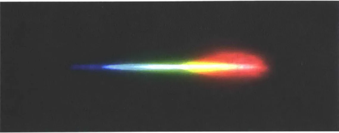
Figure 2.4: Real image of white light continuum generated in our setup.
the crystal optical axis to achieve a phase matching condition. The first amplification stage typically produces total pulse energy of 1 vtJ (signal and idler).
In the second amplification stage, the amplified beam is directed to the second nonlinear crystal (Crystal 2) and meets the 90% pump beam. Similarly, the amplification efficiency is tuned by varying the second pump delay (Delay 2) and by rotating the crystal axis. This OPA is capable of producing total output energy of 45 tJ (signal + idler) with efficiency of 20% when the idler wavelength is set to 2.1 ptm. The output of this OPA is used as the pump pulse in transient absorption setup because it can provide a tunable pump wavelength at high peak intensity.
2.1.4. White light continuum
White light continuum generation is a nonlinear optical process that converts laser pulses with narrow spectral bandwidth into pulses with very broad spectral bandwidth. For instance, in our setup we use a near infrared laser pulse that is focused into a transparent nonlinear medium to generate a visible white beam when projected on the screen (Fig 2.4). This phenomenon was first observed by R. Alfano and S. Shapiro in 1970 [21]. Such a spectral broadening is driven by the nonlinear effects of self-phase modulation (SPM). This results from the Kerr nonlinearity of materials that also gives rise to Kerr self-focusing. We discuss this briefly as follows. Laser pulses with a gaussian intensity time profile is given by
(a)
(b) Time
Time
Figure 2.5: (a) Laser pulse with a gaussian temporal profile. (b) Frequency shift due to self-phase modulation after passing through a transparent nonlinear medium.
t 2
I(t) = Io exp ( ) (2.1)
where Io is the peak intensity and T is the l/e pulse duration (Fig 2.5a). At high intensity,
laser pulses that are traveling inside a medium can induce a refractive index change
n(I) = no + n21 (2.2)
where no is the linear refractive index and n2 is the nonlinear refractive index due to X(3)
nonlinearity of the medium. The electric field of an incident laser pulse propagating in vacuum in Z direction can be expressed as E(t) = Eo cos(kz - wt). The time-varying laser
intensity results in a time-varying refractive index of material n(t), leading to a phase shift of the pulse's electric field
2rwn(t)
0p(t) = wt - kz = wot - ) L (2.3)
jAo
where wo and Ao are the carrier frequency and vacuum wavelength of the pulse, and L is the distance the pulse has traveled. The time-varying phase shift results in a time-varying frequency shift of the pulse (Fig 2.5b), and the instantaneous frequency is given by
Sapphire
White light
+-L
Figure 2.6: Incoming near IR laser pulse undergoes a self-phase modulation inside a sapphire
glass, resulting in an outgoing white light continuum with a linear chirp.
d4(t) (47rLnl2IO \ t2 (.
w(t) dt ( + -T2 t ex (2.4)
We can analyze the frequency shifts in three different time segments. The leading edge of the pulse shifts to lower frequencies (red-shifted), the trailing edge shifts to higher frequencies (blue-shifted), while the center exhibits no frequency shift. Although the carrier frequency o(t) varies in time, the envelope temporal profile is effectively unchanged. Thus the spectral broadening maintains the incident pulse duration. However, the effect of group velocity dispersion through a transparent medium still occurs. In medium with normal dispersion, the red leading edge of the pulse travels with a faster group velocity, while the blue trailing edge with a slower group velocity. This effect spreads the frequency components temporally, an effect known as chirp, which can be as wide as 1 picosecond for wavelength range of 500-700 nm (Fig 2.6). Nevertheless, the individual packets of frequency components still maintain the femtosecond pulse duration of the incident pulse, which is an important criterion for ultrafast transient absorption experiment.
In the above discussion, we have shown that self-phase modulation in the time domain can result in a white light continuum generation. Meanwhile, self-phase modulation in the spatial domain can also result in a distinct appearance of the white light pattern on the screen. The continuum appears as a round white disk surrounded by a concentric rainbow-like pattern (Fig 2.7a-d). This is called a conical emission and it exhibits a large divergence angle. This is similar to the Kerr self-focusing effect except now we have multiple different wavelengths in the continuum.
Figure 2.7: Capturing the conical emission feature. (a) Full intensity white light continuum. (b)
Reduced intensity white light continuum, showing the rainbow-like pattern due to conical emission. (c) Orange color component after using 590 nm band pass filter. (d) Red color component after using 660 nm band pass filter.
2.2. Data analysis
Throughout our analysis, we used the proper definitions of reflectance R, transmittance T and absorptance a, which respectively means the fractions of incident electromagnetic power that is reflected, transmitted and absorbed at the monolayer interface (between vacuum and substrate). This is in contrast to reflectivity and transmittivity, which are technically only valid for semi-infinite system. We also used more familiar names such as absorbance and absorption to mean, quantitatively, the absorptance
a of monolayer TMDs.
Pump-probe experiments detect small changes in probe reflectance (or transmittance) that is induced by pump excitation. This gives the differential reflectance
AR/R as a function of energy and time delay, from which we can obtain the transient
reflectance, R(t) = R0(1 + AR(t)/RO), where Ro is the reflectance of the system in equilibrium. In fact, the absorptance a (or the induced absorptance Aa) is what we really want (as shown in the main text) because it provides the explicit information about the optical transition matrix element of the system. The absorptance and the reflectance are related through the complex dielectric function J. This relation can be derived using Maxwell equations shown in section 2.2.2. We obtain 9(o, t) by fitting R(o, t) using a Kramers-Kronig (KK) constrained variational analysis [22] shown in Section 2.2.1. Finally, we construct a(o, t) by repeating this procedure at different time delays. The details of the above procedure are described as follows, in the case for monolayer TMD WS2.
2.2.1. Kramers-Kronig analysis
First, we want to find the relation between the complex dielectric function and the optical properties such as reflectance, transmittance and absorptance by using Maxwell's equations. It is important to include the substrate influence on electromagnetic radiation especially for atomically-thin materials. Here, the current density in a monolayer WS2
sample is described by a delta function,
jx
= d(o))(z)E, where d is the complexconductivity and Ex is the x-component of the probe electric field (along the sample's surface). By substituting this into Maxwell's equations and using the appropriate boundary conditions between the monolayer and the substrate, we can obtain the reflectance as
(1 - - 2 + ( 21(Ej - 1))2
R (w) = (2.5)
(1 + n+ E2) + +( (E1 - 1))2
and the transmittance as
T (w)=4 (2.6)
(1 + nS + 762)2 + ( (El - 1))2
where ns is the substrate's refractive index (1.7675 for sapphire at photon energy of 2.07 eV), d is the effective thickness of the monolayer (0.67 nm), E, and E2 are the real and
imaginary parts of the dielectric function, respectively. Here, the 2D dielectric function is expressed as
4mi3/d
+(o) = 1
id+(2.7)
Meanwhile, the absorptance can be expressed as
4 wdE2
a(o) = (2.8)
) +
n,(1
+ 7E2) + (w(Ej - 1))2These expressions are exact, and they are valid for any monolayer materials on a dielectric substrate. We find that the presence of the substrate significantly influences the optical properties of the monolayer WS2 above it. As compared to an isolated monolayer
WS2, the reflectance is enhanced, while both the transmittance and the absorptance are
reduced. In graphene, the above expressions can be further simplified because the real part
of its dielectric function is featureless in the visible spectrum (El ~ 1, negligible q2). This is,
however, not the case for monolayer WS2, and we must include both the real and imaginary
,parts of the dielectric function to obtain accurate results. In situation where none of the equilibrium absorptance, reflectance or transmittance spectrum is available, the pump-induced absorptance Aa can still be estimated from the measured AR/R or AT/T through the following expression
AR (ns+ 1 )+ s
(,y2]+
y2) (. = + 1 2 (2.9) S- (ns Y2 AT ns+l (y2+y2) - = + + Aa (2.10) T 24Y2Iwhere AR and AT are the pump-induced changes of the probe reflectance R and transmittance T, ns is the refractive index of the substrate, yi = aod(El - 1)/c, and
Y2 = wdE2/C. In situation where y2 and y2 are small, such as graphene and few other
TMDs, only the first term in the bracket needs be considered.
In our analysis, we used the equilibrium absorptance a of monolayer WS2 measured using differential reflectance microscopy. The absorptance spectrum contains peaks from the A exciton at 2.0 eV. The equilibrium reflectance Ro can then be constructed from a by finding the appropriate complex dielectric function j as expressed in Equations 2.7 & 2.8. To do this, we implemented a Kramers-Kronig (KK) constrained variational analysis [22] to extract j from the measured a in thin-film approximation. Here, the total dielectric function is constructed by many Drude-Lorentz oscillators, which are anchored at equidistant energy spacing, in the following form
N 2
+)= E(2.112,k
k=1 0 yk
In our calculations, we used N = 40 oscillators with a fixed linewidth of Yk = 50 meV
spanning the energy range of 1.77 eV OO,k 2.40 eV, and we found that these
parameters can fit a spectrum very well. We can then construct Ro spectrum by using J obtained from the above analysis.
The transient absorptance spectra a(t) can be obtained by performing similar (KK) analysis. This time we inferred the absorptance from the reflectance at different time delays: R(t) = RO(1 + AR(t)/RO), where the differential reflectance AR(t)/RO is measured
directly from the experiments.
2.2.2. Maxwell's equations for monolayer sample
In this section, we provide a full derivation from Maxwell's equations in order to obtain the exact solutions of reflectance R (w), transmittance T(w) and absorptance spectra
a(w) for any monolayer materials on a substrate. Readers who are interested in this
section should also refer to the original articles by L. A. Falkovsky [23] and T. Stauber [24] in the study of graphene. Here, we express the solutions in terms of the complex dielectric function E(o) or conductivity d(w) for Kramers-Kronig analysis shown in previous section.
The electromagnetic wave equation at frequency a), inside a medium with a dielectric constant e and a current density
j,
can be expressed asV(V - E) E = 2 E + C2 j (2.12) We consider a situation (Fig 2.8) where the monolayer medium spreads on the xy plane with a current density
j,
= j(w)6(z)Ex(x, t) that is driven by a propagating electric fieldon the xz plane of the form E = (E0 , 0, Eoz)e (kr-t). By evaluating the partial derivatives of E, the two components of the wave equation can be expressed as
dE~ O2EX w 4wicv
z 2 -e-E = ix (2.13)
ik Z dz Z2 C 2 Ex C2j
ikx a* + k - 1E to 2Ez = 0 (2.14)
az
(X C 2where we have used 0/Ox -> ikx because the law of refraction requires that kx is
conserved, while kz is not. Boundary conditions for the tangential and normal components of the field (red arrows) yield
Ex = (E - Er) cos 61 = Et cos Ot (2.15)