Controlling Nanomaterial Self-Assembly for Next Generation
Optoelectronic Applications
by
Mark Clayton Weidman Bachelor of Chemical Engineering
University of Delaware, 2011
SUBMITTED TO THE DEPARTMENT OF CHEMICAL ENGINEERING IN PARTIAL FULFILLMENT OF THE REQUIREMENTS FOR THE DEGREE OF
DOCTOR OF PHILOSOPHY IN CHEMICAL ENGINEERING at the
MASSACHUSETTS INSTITUTE OF TECHNOLOGY February 2017
© 2017 Massachusetts Institute of Technology. All rights reserved.
Signature of Author: _____________________________________________________________________________________________________________________________
Department of Chemical Engineering September 28th, 2016
Certified by: _________________________________________________________________________________________________________________________________________
William A. Tisdale Charles and Hilda Roddey Career Development Professor of Chemical Engineering Thesis Supervisor
Accepted by: ________________________________________________________________________________________________________________________________________
Daniel Blankschtein Herman P. Meissner Professor of Chemical Engineering Chairman, Committee for Graduate Students
3
Controlling Nanomaterial Self-Assembly for Next Generation
Optoelectronic Applications
by
Mark Clayton Weidman
Submitted to the Department of Chemical Engineering on September 28th, 2016 in partial fulfillment of
the requirements for the degree of Doctor of Philosophy in Chemical Engineering
Abstract
Semiconductor nanocrystals, also known as quantum dots, are an exciting class of materials because their band gap can be tuned according to the nanocrystal size. In this way, the material band gap can be largely decoupled from its atomic composition – a property unique to this system. The potential applications for semiconductor nanocrystals are wide ranging and include: LEDs, photovoltaics, photon downconversion, photon upconversion, and thermoelectrics. However, their size-dependent band gap can also be a hindrance, as any size variation in the ensemble of nanocrystals introduces energetic disorder and spatial disorder in films. While synthesized as a colloid, for most applications the nanocrystals are deposited as a thin film. The rate of energy transfer between nanocrystals in the film, dictated by the arrangement and distance between neighbors, is therefore a critical parameter affecting device efficiency. As a result, controlling the nanocrystal physical arrangement is crucial to the success of these materials. Despite this, there is a lack of understanding of how to observe and control these processes at the nanoscale.
This thesis begins by improving the synthesis of lead sulfide (PbS) nanocrystals to produce narrow size dispersity ensembles with tunable average size by ensuring the reaction is diffusion-limited. We then experimentally determine what parameters (ligand coverage, solvent, size dispersity) most affect the ability of these nanocrystals to self-assemble into highly ordered superlattice structures. We show that superlattices can be produced with a wide variety of surface ligands of differing lengths, either directly from a colloidal suspension or post-deposition and we thoroughly characterize the interparticle spacing as a function of ligand species. Next, we demonstrate an in situ X-ray scattering technique which enables the real-time visualization of nanocrystal self-assembly, with details unprecedented by any other experimental method. This technique led to a better understanding of the colloid to superlattice transition, including the observation of intermediate states and the ability to compare kinetics of different self-assembly aspects. Finally, we present experimental measurements demonstrating that nanocrystal size dispersity and self-assembly are critical to efficient energy transfer in films and that as energetic disorder is minimized through improved synthetic methods, spatial disorder becomes an increasingly important parameter to control. In the final experimental chapter of this thesis, we apply this knowledge to a different material system – perovskite nanoplatelets, which have the potential to be useful as an inexpensive, solution-processable emission material. For these 2D materials, we optimize the thickness homogeneity and study the self-assembly of the nanoplatelets into stacked superstructures. We highlight the incredible tunability of this material system accessible through thickness and compositional tuning, which allows absorption and emission to be shifted across the entire visible range. Lastly, we demonstrate the potential of this system for next generation LEDs.
Thesis Supervisor: William A. Tisdale
5
Acknowledgements
There are many, many people I want to thank who have contributed in some way to this thesis. First, there are funding agencies that have made this work possible through their financial support: NSF GRFP, US Department of Energy, Center for Excitonics, and MIT Energy Initiative.
My passion for math and chemistry was first encouraged by two incredible teachers in high school, Dr. John Sohn and Mr. Christopher Bibeau. During my undergrad studies at the University of Delaware, I found that chemical engineering was a perfect combination of both these subjects. It was also at UD when I first started doing research in the lab of Dr. Jingguang Chen. Dr. Chen was an outstanding teacher and research advisor who gave me interesting projects in his group and encouraged me to pursue grad school. He also paired me with Dan Esposito, then a graduate student in his group, who became my research mentor. Dan was incredibly patient, enthusiastic, and generous with his time. His teaching was instrumental in my development as a researcher and my path towards grad school.
My thesis advisor, Will, has made all of this work possible. Joining his just-started lab at MIT was the best decision I made in my grad school career. Will’s enthusiasm and excitement for science is rivaled only by his commitment to quality. Will puts his students’ best interest before his own and allows his students to focus solely on research with the flexibility to explore any project which interests them. Will has initiated many productive collaborations for me, enabled me to attend conferences, and encouraged me to apply for scholarships. He leads by example and everyone in the lab has become better at presenting their work and making it understandable to a wide audience as a result of his teaching. Being a part of Will’s lab has also been a very enjoyable time – from our annual dinners, Jamboree, group meetings – Will has cultivated a friendly atmosphere that emphasizes a happy work-life balance. Will is someone who never seems to have a bad day and I am truly fortunate to have had an advisor as great as him.
This work has also been guided by my two excellent committee members. Professor Olsen was first to suggest doing X-ray scattering measurements, which proved to be a staple of this thesis. Additionally, his Structure of Soft Matter class helped me to better understand many of the processes and characterization techniques related to nanocrystals. Professor Bulović always provided excellent suggestions in our meetings, made his lab resources readily available, and helped foster collaborations with his group members, particularly in relation to our perovskite study. He has also been a role model for how to address the big problems facing the world and how to make science accessible to the public.
With that in mind, I want to thank the members of the Bulović and Bawendi labs at MIT. Though we work on similar projects, both labs have been extremely inviting and inclusive to me. The Bawendi lab was even gracious enough to let me work in their wetlab while ours was still being constructed. Dong-Kyun Ko was the person who first showed me how to make nanocrystals. Chia-Hao Chuang, Darcy Grinolds, and Jenn Scherer helped me better understand PbS synthesis and measure the properties of my materials. Joel Jean and Farnaz Niroui trained me on several important instruments in their lab related to this work. Sam Stranks was a valuable source of knowledge for perovskites and helped measure some of their properties. Parag Deotare helped us setup our exciton diffusion imaging and was critical to getting it working in the infrared. I had the privilege of working with several talented undergraduate students during my time at MIT. Megan Beck was instrumental in developing our synthesis methods, Victoria Petrova helped develop our in situ monitoring capability, and Quan Nguyen developed our solution-phase ligand exchange procedure with great care. I am excited to see what lies ahead for these very talented students.
6 I also was able to work with two excellent Masters students from ETH Zurich: Robert Keitel, who shed light on the thermal properties of our PbS nanocrystals and their applicability for thermoelectrics and Michael Seitz, who contributed significantly to all the perovskite work and notably developed our tin-based perovskites.
A large portion of the results in this thesis were measured at synchrotron beamlines. I want to thank the beamline operators, who were both fantastic resources for understanding this technique. Kevin Yager at Brookhaven National Laboratory helped me immensely to understand the data when I first started doing these measurements and to explore novel techniques. Detlef Smilgies at the Cornell High Energy Synchrotron Source helped us to do time-resolved scattering measurements and understand the data. He was very generous with giving us beamtime and was always fun to talk to during long measurement sessions.
I owe a huge debt of gratitude, both in terms of research contributions and friendship, to the members of the Tisdale Lab. That starts with Ferry Prins, who was the first post-doc in the lab and had a huge influence on the first group of grad students. Ferry not only had great ideas but also had seemingly unending patience when teaching. More so, Ferry became a mentor and a friend and I will always remember our trips to the Muddy’s and seeing the Rolling Stones with him. Rachel Gilmore and Jolene Mork were the other first members of Will’s group and helped to get this lab started and establish a good lab culture. Rachel has contributed significantly to this thesis and her excellent work has helped justify my self-assembly research. Jolene has always been a useful resource, especially for her vast chemistry knowledge, as well as a fun lab member. Matt Ashner helped setup the diffusion imaging measurements and has been a great source of knowledge relating to optics. Aaron Goodman has always given helpful suggestions in lab and for presentations and has been an excellent friend to have in lab. Of course, Buddy (Aaron’s dog) has provided me with endless joy over the past few years. Dan Congreve joined the lab as a post-doc during the last year and has been a source of knowledge relating to nanomaterial device work and a fun person to collaborate with. I thank Dan for his work on the layered perovskite LEDs that he has allowed to be used here. Barb has been an amazing admin for the group and help enormously with getting us whatever we need and has also been a fun and caring person to talk with. I want to thank the other members of the lab – Lisa, Liza, Nabeel, Oat, Pooja, Sam, SK, and Yunan – for making this a great lab to work in over the last five years.
I want to thank my amazing group of friends at MIT who have made these last five years truly special. I am lucky to have met new friends from all over the country and all over the world. We have had great times together exploring Boston and vacationing in places like Las Vegas, San Diego, Austin, Prague, Budapest, and Tokyo. My friends were there for all the good times but also there for me when I needed support and encouragement when we were all adjusting to life here as first year students. A sincere thank you to David, Eric, Helen, Karthik, Lionel, Rosanna, Sean H., Sean F., Steven, Thomas, Tony, William, and Xiao.
I also want to thank my high school friends Anker and Bryan for helping me to relax and forget about research for a while and always cracking me up. My college roommates Rich and Alex were always quick to come visit and made sure we had a great time. I also want to thank Cara for her support and friendship as we both navigated grad school at the same time.
My beautiful girlfriend Jen has been a huge supporter and always been understanding about my research schedule. Jen is proud of and interested in my research, but more importantly she gives me something to look forward to and can always make me laugh.
7 I want to thank my family members – Uncle Scott, Aunt Linda, Amanda, and Rebecca. Scott and Linda have set a great example of why to pursue higher education and have visited me whenever they are nearby Cambridge. Scott has always been very interested in my work and has given me useful guidance throughout. JJ and Betsy have looked after me ever since I came to Cambridge and came to visit frequently to take me out for lunch. They made it clear that their home was always open to me, and I sincerely thank them for that peace of mind. Lori, Mike, and Collin have supported every goal of mine since I was just a kid and never failed to let me know they were proud of me. They bring joy to my whole family and our lives are so much better because they are a part of it. The Budgies – Dave, Von, Lindsey, and Jeanno – have been like a second family to me. They are always there for me when I need them and will always be a special part of my life. And lastly, my Mom and Dad. None of this would have ever been possible without them. They never fail to put my best interests above their own and have given me their love and support with every decision I have made. For that I can never thank them enough.
9
Table of Contents
Chapter 1 – Introduction ... 19
1.1 – Nanocrystal History and Physics ... 20
1.2 – Importance of Size Dispersity ... 23
1.3 – Importance of Self-assembly ... 23
1.4 – X-ray Scattering ... 25
1.5 – Perovskite Nanoplatelets ... 26
1.6 – Thesis Overview ... 28
Chapter 2 – Minimizing Size Dispersity in PbS Nanocrystals ... 29
2.1 – Introduction ... 30
2.2 – Nanocrystal Growth Theory... 30
2.2 – Quantifying Size Dispersity ... 31
2.3 – Monodisperse Growth Mechanism ... 33
2.4 – Nanocrystal Purification ... 35
2.5 – Nanocrystal Sizing Curve ... 36
2.6 – Photoluminescence Properties ... 38
2.7 – Self-assembly ... 40
2.8 – Conclusions ... 42
2.9 – Experimental Methods ... 43
Chapter 3 – Making Superlattices ... 47
3.1 – Introduction ... 48 3.2 – Solvent ... 48 3.3 – Size Dispersity ... 50 3.4 – Ligand Coverage ... 52 3.5 – Ligand Length ... 53 3.6 – Conclusions ... 55 3.7 – Experimental Methods ... 56
Chapter 4 – Ligand-Exchanged Superlattices ... 59
4.1 – Introduction ... 60
4.2 – Monodisperse PbS Nanocrystal Size Series ... 60
4.3 – Self-assembly with Native Ligands ... 61
10
4.5 – Interparticle Spacing Analysis ... 68
4.6 – Avoiding Cracking ... 71
4.7 – Conclusions ... 72
4.8 – Experimental Methods ... 73
Chapter 5 – Watching Self-assembly ... 75
5.1 – Introduction ... 76
5.2 – Characterizing the Initial and Final States ... 77
5.3 – Observing Self-assembly in Real-time ... 80
5.4 – Kinetics of Superlattice Transformation ... 82
5.5 – Conclusions ... 86
5.6 – Experimental Methods ... 87
Chapter 6 – Correlating Energy Transfer with Film Structure... 89
6.1 – Introduction ... 90
6.2 – Charge Carrier Dynamics ... 90
6.3 – Exciton Diffusion Imaging ... 95
6.4 – Spectrally, Temporally Resolved Photoluminescence Measurements ... 98
6.5 – Conclusions ... 99
6.6 – Experimental Methods ... 100
Chapter 7 – Perovskite Nanoplatelets ... 101
7.1 – Introduction ... 102
7.2 – Nanoplatelet Synthesis ... 104
7.3 – Nanoplatelet Characterization ... 106
7.4 – Varying Metal (B) and Halide (X) Components ... 110
7.5 – Varying Cation (A) Component ... 111
7.6 – Continuous Halide Tunability ... 114
7.7 – Layered Perovskite LEDs ... 117
7.8 – Conclusions ... 119
7.9 – Experimental Methods ... 120
Outlook ... 123
List of Publications ... 125
11
List of Figures
Figure 1.1 Lycurgus Cup, made of glass with embedded gold nanocrystals, appears different colors depending if it is illuminated from outside the cup or inside the cup. Reproduced with permission.1 ... 20
Figure 1.2 Semiconductor nanocrystals exhibit quantum confinement, giving them tunable properties intermediate of those of the bulk state and single atom state. ... 21 Figure 1.3 Size-series of semiconductor nanocrystals under ultraviolet illumination. Reproduced with permission.6 ... 22
Figure 1.4 (a) atomic depiction of a typical nanocrystal core with bound surface ligands. (b) high-resolution TEM image of single nanocrystal with visible lattice fringes due to the crystalline atomic lattice. (c) low magnification TEM image of a nanocrystal array, with separation between the nanocrystal cores as a result of the surface ligands. ... 22 Figure 1.5 Schematic illustrating a monodisperse and polydisperse ensemble of particles, and how – when nanocrystal size determines its band gap – ensemble size dispersity can play a large role in performance. ... 23 Figure 1.6 SEM image of body-centered cubic PbS nanocrystal superlattice showing long-range ordering. Inset is the superlattice top layer – an exposed (110) close-packed plane. ... 24 Figure 1.7 Entropic relationship between the two states – colloid and superlattice – as a function of the volume fraction of nanocrystals in the solvent. The crossover around 55% volume fraction indicates when spontaneous crystallization can occur... 25 Figure 1.8 Depiction of X-ray scattering geometry for simultaneous 2D GISAXS and GIWAXS pattern collection from a thin film of nanocrystals. ... 25 Figure 1.9 Efficiency of photovoltaic devices over time based on active material: single-crystal silicon, organics, and perovskites. Source: NREL. ... 26 Figure 1.10 Representations of the different metal halide perovskite allotropes: (a) bulk perovskite unit cell and typical constituent ions, (b) cubic nanocrystal, and (c) nanoplatelet. ... 27 Figure 1.11 Stages of self-assembly characterized by electron microscopy. (a) TEM image of a single PbS nanocrystal (b) TEM image of a 2D monolayer of PbS nanocrystals. (c) TEM image of a 3D body-centered cubic superlattice of nanocrystals. (d) SEM image of nanocrystal superlattices highlighting the extensive long-range ordering observed. ... 28 Figure 2.1 Typical hot-injection synthesis scheme. (a) Separate reaction precursor solutions just prior to the injection step. (b) Reaction flask post-injection, showing an immediate color change from clear to black (indicating IR absorbing nanocrystals). (c) Stages of nanocrystal growth as a function of time and precursor concentration, according to the LaMer growth mechanism. ... 31 Figure 2.2 Comparison of absorption spectra and TEM micrographs for nanocrystals having the same peak absorption wavelength but different HWHM values. ... 32 Figure 2.3 HWHM of the first absorption peak plotted versus peak wavelength for different Pb:S precursor ratios. All syntheses were performed at a reaction temperature of 120°C. The dashed gray line is the expected trend for a nanocrystal ensemble having 3.3% size dispersity. ... 33
12 Figure 2.4 Absorption spectra, plotted both in terms of wavelength and energy, using a 24:1 Pb:S precursor ratio, showing the synthetic range of 1000 – 1800 nm (1.25 – 0.70 eV). The bottom two spectra (dark violet, purple) were synthesized at 40°C and 80°C, respectively, while all others were synthesized at 120°C. Labels indicate the average diameter of the nanocrystals, as determined by the sizing curve... 34 Figure 2.5 XRD of as-synthesized nanocrystals before purification (gray) and after purification (black). The blue vertical bars are the reference PbS peak locations (ICDD PDF number 00-005-0592), inset is HRTEM of a single PbS nanocrystal with scalebar of 5 nm. ... 36 Figure 2.6 TEM images of (a) unpurified PbS nanocrystals, showing PbCl2 impurities, and (b) PbS nanocrystal
purified following the oleic acid purification scheme. ... 36 Figure 2.7 Nanocrystal band gap versus diameter, as measured by TEM and solution phase SAXS. The best-fit curve (dotted line) is given by Equation 2.2. ... 37 Figure 2.8 (a) Photoluminescence spectra for nanocrystals dispersed in tetrachloroethylene. (b) Comparison of absorption spectra (solid lines) and photoluminescence spectra (dashed lines). (c) Stokes shift plotted as a function of peak absorption wavelength. ... 38 Figure 2.9 Photoluminescence lifetime measurements for nanocrystals in solution and in thin film. An exponential fit to the solution data gives a lifetime of 1.8 µs. The 1/e lifetime of the thin film is 260 ns. .. 39 Figure 2.10 Absorption spectra for 4.7, 5.9, and 7.4 nm diameter nanocrystals before and after storage in air for 3 months. For all sizes, the peak positions and HWHM values are constant over time. ... 39 Figure 2.11 Air-stability of PbS nanocrystals over the course of 1 year, showing the absorption and GISAXS / GIWAXS remain largely unchanged. Nanocrystals were stored as a dried powder in a glovebox during the majority of the time. ... 40 Figure 2.12 Two and three-dimensional self-assembly of PbS nanocrystals. The TEM image in (a) of a monolayer shows near ideal hexagonal close packing. The TEM image in (b) shows a three-dimensional superlattice approximately 5 nanocrystal layers thick. The GISAXS pattern in (c) shows long-range ordering of a body-centered cubic superlattice. The in-plane and out-of-plane scattering vectors are denoted, with tick increments of 0.1 A-1. ... 41
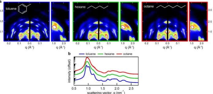
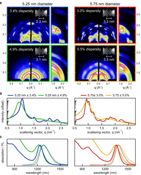
Figure 2.13 Current-voltage characteristics for a photovoltaic test cell made using PbS nanocrystals made from the method detailed in this chapter. (credit: Chia-Hao Chuang) ... 41 Figure 2.14 (a) in situ PL monitoring setup, the addition of an blue excitation LED light and fiber optic dip-probe enable the monitoring of PL during synthesis. (b) Typical spectra obtained at 2 second intervals as the nanocrystals grow in solution. (c) PL peak values as a function of growth time. ... 46 Figure 3.1 Solvent effects on self-assembly. (a) GISAXS and GIWAXS patterns for nanocrystal films spin-coated from dispersions in toluene, hexane, and octane. (b) Azimuthally integrated GISAXS patterns. .... 49 Figure 3.2 Size-dispersity effects on self-assembly. (a) GISAXS and GIWAXS patterns for 5.25 and 5.75 nm diameter nanocrystals with varying size dispersity. (b) Azimuthally integrated GISAXS patterns and (c) solution-phase absorption and photoluminescence spectra of the nanocrystal samples. ... 50 Figure 3.3 Ligand coverage effects on self-assembly. (a) GISAXS and GIWAXS patterns for samples with decreasing ligand coverage – accomplished through successive precipitations. (b) Azimuthally integrated GISAXS patterns and (c) solution-phase absorption spectra of the nanocrystal samples. ... 52
13 Figure 3.4 Ligand length effects on self-assembly. (a) GISAXS and GIWAXS patterns for nanocrystals having oleic acid, dodecanoic acid, or hexanoic acid surface ligands (decanoic acid sample not shown). Superlattice unit cells and their orientation relative to the substrate are depicted in the insets. (b) Solution-phase absorption and photoluminescence spectra of the nanocrystal samples. (c) Measured interparticle spacing (GISAXS and TEM) as a function of the number of carbons in the surface ligand species, compared to the expected interparticle spacing for the extreme cases two ligand lengths and one ligand length between neighboring nanocrystals. ... 54 Figure 4.1 Characterization of the three sizes of PbS nanocrystals used in this study. Data from the “large” diameter batch are shown in red (d = 7.3 nm), “medium” in green (d = 6.2 nm), and “small” in blue (d = 5.4 nm). All measurements have been normalized and offset for clarity. (a) Absorption (solid lines) and photoluminescence (dashed lines) spectra. (b) Solution-phase SAXS measurements. (c) XRD with reference PbS pattern (ICDD PDF no. 00-005-0592) shown in gray. (d) TEM images; scale bars are 20 nm. ... 61 Figure 4.2 SEM micrographs of spin-coated nanocrystal films made from the large diameter nanocrystals: (a) top view of an exposed BCC (110) plane, (b) top view of an exposed BCC (100) plane, (c) film with discontinuity showing the average thickness of ∼15 nanocrystals, and (d) horizon-view of a nanocrystal superlattice with exposed edge (image taken near the edge of the spin-coated sample, where film thickness is greater). ... 62 Figure 4.3 (a),(c),(e) GTSAXS patterns from spin-coated films of the three nanocrystal sizes: large diameter (red borders), medium diameter (green borders), and small diameter (blue borders). Corresponding GIWAXS patterns of the films are presented in (b),(d),(f). ... 63 Figure 4.4 Diagram of the two film deposition methods studied here. The one-step method is characterized by a thick film and 24 h ligand exchange while the layer-by-layer constitutes many thin layers with 30s ligand exchanges in between. ... 64 Figure 4.5 SEM images of 3-mercaptopropionic acid-treated films show that, while the layer-by-layer method creates a more homogeneous film, the one-step method better preserves local nanocrystal ordering. ... 65 Figure 4.6 GISAXS patterns at an incident angle of 0.3° for all three sizes of nanocrystals studied and made using the one-step method and the layer-by-layer method. From left to right the columns have ligands of oleic acid, 1,8-octanedithiol, 1,4-butanedithiol, and 1,3-benzenedithiol. Comparing between the different methods shows how ordering is better maintained using the one-step method while comparing between the different sizes of nanocrystals shows that ordering is better maintained when the ligand volume constitutes a smaller fraction of the total volume. ... 66 Figure 4.7 Comparison of the GISAXS patterns (left-hand column) and GIWAXS patterns (right-hand column) for films of large diameter nanocrystals with oleic acid ligands and 3-mercaptopropionic acid ligands. The one-step method preserves the superlattice order and the cohesive nanocrystal facet arrangement better than the layer-by-layer method. ... 67 Figure 4.8 Interparticle spacings for the ligand species studied, plotted from shortest to longest. The colored bars indicate the standard deviation among the three different core sizes used. ... 69 Figure 4.9 Experimental interparticle spacing as a function of number of carbons in the ligand for the dithiol and monothiol ligand species studied. The dashed lines are the simulated distances for these ligand ... 70
14 Figure 4.10 SEM images of ligand exchanged films spin-coated from nanocrystals initially with (a,c,e) oleic acid or (b,d,f) hexanoic acid surface ligands. Spin-coating from a suspension of hexanoic-acid capped nanocrystals then performing a ligand exchange could greatly reduce film cracking. ... 71 Figure 5.1 The disparate initial and final states of nanocrystal self-assembly. ... 76 Figure 5.2 (a) Absorption and photoluminescence of 5.6nm diameter lead sulfide nanocrystals as a colloidal suspension. (b) TEM image of a BCC superlattice of the nanocrystals with a superimposed [100]SL view of
four unit cells with a lattice constant of 9.05 nm. Inset (left) shows a high-resolution TEM image of a single nanocrystal in which the atomic planes are visible and the corresponding nanocrystal model (right) that leads to this pattern. (c) Atomic model of the nanocrystals used in this study highlighting a hexagonal (111)NC face and a square (100)NC face. The ligand coverage density has been decreased for the image to
better show the nanocrystal core. Inset shows the simplified nanocrystal representation to be used in subsequent figures. ... 77 Figure 5.3 X-ray scattering from the colloidal form (initial state) and the self-assembled superlattice (final state). (a) GISAXS and GIWAXS patterns from a colloidal suspension of the nanocrystals in toluene. Inset shows the azimuthally integrated GISAXS pattern and the fit to a 5.6nm diameter spherical form factor. (b) Illustration of randomly oriented nanocrystals in solution corresponding to the data shown in (a). (c) GISAXS and GIWAXS patterns for a spin-coated thin film of nanocrystals that have self-assembled into a BCC superlattice with atomically aligned nanocrystals. Inset shows the azimuthally integrated GISAXS pattern. (d) Illustration of two layers of the atomically aligned BCC nanocrystal superlattice on the substrate as defined by the data in (c), where the BCC (110)SL plane is parallel to the substrate. (e) Experimental
apparatus for simultaneous GISAXS and GIWAXS measurement during controlled solvent evaporation. .. 78 Figure 5.4 GISAXS patterns for the final BCC superlattice overlaid with the expected scattering peaks (white dots) for BCC superlattices with different planes parallel to the substrate plane. The (110)SL parallel case
matches the experimental scattering peaks. ... 79 Figure 5.5 GIWAXS patterns for the final orientationally-aligned BCC superlattice overlaid with the expected scattering peaks (white dots) for an atomic PbS crystal with different planes parallel to the substrate plane. The (110)PbS parallel case matches the experimental scattering peaks. ... 79
Figure 5.6 Time-resolved X-ray scattering reveals the transition from a disordered colloid to a highly ordered superlattice. (a–h) Temporal evolution of GISAXS (square panels) and GIWAXS (vertical panels) patterns during the in situ measurement of nanocrystal self-assembly. The GISAXS patterns show the transition from a colloidal suspension to an FCC superlattice to a BCC superlattice via contraction of the c axis. The white circles on the left halves of the GISAXS patterns are the predicted scattering locations for the superlattice parameters indicated above each image. The GIWAXS patterns show the early onset of orientational alignment as well as the shape transformation of the 200NC scattering peak. ... 81
Figure 5.7 Visualizing the FCC to BCC transition with unit cells. Simplified model showing the transition between (a) an FCC superlattice and (b) a BCC superlattice. Two FCC unit cells are shown in blue while the BCC unit cell is shown in red. ... 82 Figure 5.8 Kinetics of structural rearrangement during self-assembly. (a) Contraction of the c axis results in an FCC to BCC transition through the BCT intermediate phase. (b) Plane alignment of neighboring nanocrystals occurs early in the self-assembly process and is maintained thereafter. (c),(d) The
surface-to-15 surface distance between nanocrystals (c) and the nanocrystal/superlattice tilt (d) change in accordance with the superlattice kinetics given in (a). ... 82 Figure 5.9 Time-evolution of GIWAXS intensity versus angle (relative to the sample horizon), showing the single peaked nature of the (111)NC scattering peak and the initially dual-peaked nature of the (200)NC
scattering peak, which merges to a single peak over time. ... 83 Figure 5.10 Characterizing nanocrystal tilt relative to the substrate by using low symmetry atomic planes. The tilt is calculated based on the angle between the low symmetry plane and the nanocrystal (110)NC
plane. ... 84 Figure 5.11 Overall depiction of nanocrystal self-assembly highlighting the transition from FCC to BCC superlattice states. The top depiction shows how the nanocrystals move relative to the substrate; the bottom images highlight how the superlattice unit cell changes relative to a fixed orientation in space. The blue axes connect the nanocrystals that make up the FCC unit cell, whereas the red axes connect the nanocrystals that make up the BCC unit cell. ... 85 Figure 6.1 Transient absorption schematic. An excitation pump is initially absorbed by the sample followed by a broadband probe pulse to determine the absorption spectrum of the sample. The time delay between these two pulses is varied to determine the transient absorption profile. ... 91 Figure 6.2 Schematic showing the redshift of the average charge carrier energy as a result of preferential hopping to lower energy nanocrystals. This redshift is proportional to the amount of size dispersity in the sample and the inhomogeneous linewidth. ... 91 Figure 6.3 (a) Absorbance (solid lines) and photoluminescence (dashed lines) of solution-phase PbS nanocrystals with varying size dispersity. (b) Absorbance linewidth (standard deviation) as a function of peak energy. The dashed lines show the estimated size dispersity of the ensemble, assuming a delta function homogeneous linewidth (method detailed in Chapter 2). ... 92 Figure 6.4 TA spectra ethanethiol treated nanocrystal films made from (a) “polydisperse” and (d) “monodisperse” ensembles. Overlaid solid lines are the steady-state absorption spectra. Dashed lines show the bleach peak position as a function of time. (b, e) Spectral slices at selected times showing the more pronounced redshift of the bleach peak in the polydisperse sample compared with the monodisperse sample. (c, f) Peak bleach position as a function of time. ... 93 Figure 6.5 (a) Homogeneous linewidth (standard deviation) for the absorbance and photoluminescence spectra, calculated from the total linewidth and the fitted inhomogeneous linewidth. (b) Average hopping time as a function of nanocrystal diameter. The hopping rate is much slower samples with higher size dispersity, and the hopping rate increases as NC size decreases. ... 94 Figure 6.6 (a) Hopping times from Figure 6.5c plotted vs center-to-center NC spacing, rather than NC diameter. (b) The hopping rate decreases with increasing center-to-center spacing. (c) Even after accounting for a greater distance travelled per hop, mobility and diffusivity decrease with increasing center-to-center NC spacing. ... 94 Figure 6.7 Contribution of energetic disorder to the average hopping time – the other major influencing factor is the center-to-center distance... 95 Figure 6.8 Exciton diffusion measurement setup. In a microscope, a nearly diffraction-limited laser pulse excites a small area of a nanocrystal film (~400 nm FWHM). The photoluminescence is collected and
16 magnified such that an APD, with active area smaller than the emission spot, can be physically scanned through the emission spot to resolve how it spreads with time. Courtesy of Aaron Goodman. ... 96 Figure 6.9 Exciton diffusion imaging of PbS nanocrystals with oleic acid ligands and hexanoic acid ligands. TEM images of the samples show the excellent self-assembly properties of both samples and the large different in interparticle spacing. We present both the short-time dynamics (exciton diffusion regime) and long-time dynamics (non-diffusive population)... 97 Figure 6.10 (a) Standard deviation of Gaussian fits to the emission peak at each time step and (b) fractions of excitons surviving versus the exciton diffusion length of those excitons. ... 98 Figure 6.11 Separation of the diffusive population and non-diffusive populations based on emission position and time. ... 98 Figure 6.12 (a) Short and long-time dynamics of the photoluminescence spectrum, as compared with the steady-state spectrum. (b) Plot of the photoluminescence peak emission as a function of time after the laser excitation, showing two distinct regimes like that found in the exciton diffusion imaging measurement. ... 99 Figure 7.1 (a) Bulk perovskite unit cell (white cube) and the chemical species used for A, B, X, and L in this study. (b) Perovskite nanoplatelets of thicknesses n = 1 and n = 2, where n represents the layers of metal-halide octahedra and n-1 represents the number of complete unit cells incorporated in the nanoplatelet thickness. ... 102 Figure 7.2 Absorption spectra from bulk MAPbBr3 polycrystalline film and from L2[MAPbBr3]PbBr4 (n=2)
nanoplatelets in toluene, showing free-charge carrier-like absorption and excitonic-like absorption, respectively. Diagram showing how the thin dimension of the nanoplatelets leads to low dielectric screening and a large exciton binding energy, in comparison to the bulk case which exhibits the opposite behavior. ... 103 Figure 7.3 Schematic of non-solvent crystallization used for nanoplatelet synthesis. ... 104 Figure 7.4 Sequential images taken during the dropwise addition of precursors in DMF to a toluene solution, resulting in the formation of perovskite nanoplatelets that exhibit blue photoluminescence. Total elapsed time for the image series was less than one second. ... 105 Figure 7.5 Solution and thin film photoluminescence for L2[FAPbBr3]PbBr4 nanoplatelets. Insets show
photographs of samples under an ultraviolet lamp. ... 105 Figure 7.6 Perovskite nanoplatelets of varying thicknesses – note the shoulders present in n > 2 thickness spectra, which result from the difficulty of controlling nanoplatelet thickness homogeneity. ... 106 Figure 7.7 TEM images of n = 1 and n = 2 thickness nanoplatelets, L2[ABX3]n-1BX4, with A = FA, B = Pb or Sn,
and X = Cl, Br, or I. ... 107 Figure 7.8 (a) XRD patterns for n = 1 (L2PbBr4) and n = 2 (L2[FAPbBr3]PbBr4) nanoplatelets showing periodic
reflections from nanoplatelet stacks which form in thin film samples (indicated by diamonds). Black circles indicate peaks corresponding to the bulk perovskite unit cell. Sections of the XRD patterns have been scaled to better show the peaks at larger angles. The XRD patterns indicate a stacking distance of 1.7 nm and 2.3 nm for n = 1 and n = 2, respectively, regardless of chemical composition. (b), (c) Schematic representations of the nanoplatelet stacks and relevant distances. ... 108
17 Figure 7.9 XRD patterns for L2PbBr4 nanoplatelets where the ligand species, L, was either octylammonium
(OA), butylammonium (BA), or an equimolar mixture of the two (BA/OA), which results in changes to the nanoplatelet superlattice stacking distance. ... 109 Figure 7.10 (a) Solution phase absorption (dotted lines) and photoluminescence (solid lines) spectra for n = 1 and n = 2 nanoplatelets in toluene, highlighting the changes which occur when the halide (X) is changed from Cl to Br to I and when the metal (B) is changed from Pb to Sn. ... 110 Figure 7.11 Nanoplatelet suspensions in toluene under ambient lighting and ultraviolet lighting. ... 111 Figure 7.12 Absorption and photoluminescence spectra for n = 2 nanoplatelets in toluene with varying cation (A) species for (a) L2[APbBr3]PbBr4 nanoplatelets and (b) L2[APbI3]PbI4 nanoplatelets. ... 112
Figure 7.13 (a) Absorption spectra for n = 1 and n = 2 nanoplatelets showing continuous tunability as a function of halide composition. Mixtures were made between Cl/Br and Br/I in increments of 10% between the pure compositions. (b) Absorption peak as a function of halide composition. (c) Photoluminescence of n = 2 nanoplatelets for all Br/I mixtures and from 100% Br to 50/50% Cl/Br, with trace colors reflecting the color of emission. All Absorption and photoluminescence measurements were taken in solution phase (toluene). ... 115 Figure 7.14 Stability of nanoplatelets under exposure to (a) ambient laboratory conditions – air and humidity effects – and (b) ultraviolet light (~10 mW). ... 116 Figure 7.15 (a-d) Absorption (solid line) and photoluminescence (dashed line) of the layered methylammonium lead halide perovskite films, where X is the halide used in the mixture and L is the stoichiometric excess of the butylammonium ligand species separating the layers (stoichiometric = 100%). (e) X-ray diffraction measurements, showing periodic reflections at 4.6° (1.94 nm d-spacing) and 6.5° (1.36 nm d-spacing), corresponding to the thickness of the n = 2 (diamonds) and n = 1 (circles) layered perovskites, respectively. Courtesy Daniel Congreve. ... 118 Figure 7.16 Electroluminescence from 2D quantum-confined layered perovskite light emitting devices. Bulk photoluminescence spectra are shown for reference in the dashed lines. Courtesy Daniel Congreve... 118
18
List of Tables
Table 2.1 Reaction guidelines for PbS nanocrystal synthesis. ... 35
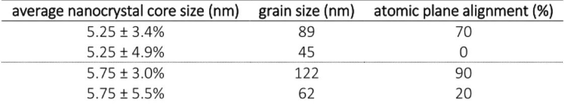
Table 3.1 Grain size and Atomic Plane Alignment for Variable Solvent Samples. ... 49
Table 3.2 Grain size and Atomic Plane Alignment for Variable Size Dispersity Samples. ... 51
Table 3.3 Grain size and Atomic Plane Alignment for Variable Ligand Coverage Samples. ... 53
Table 4.1 Interparticle spacing for the two deposition methods and ligand species studied, averaged over the three different nanocrystal sizes. ... 68
Table 5.1 FCC superlattice unit cell parameters used for indexing the GISAXS patterns in time. ... 88
Table 7.1 Summary of absorption and emission properties of perovskite nanoplatelets (L2[ABX3]n-1BX4) and bulk, polycrystalline perovskite (ABX3) phase (denoted n = ∞). ... 113
Table 7.2 Photoluminescence quantum yield (PL QY) of select nanoplatelets. ... 114
19
20
1.1 – Nanocrystal History and Physics
The influence of nanocrystals – materials with bulk-like atomic lattices but physical dimensions <100 nm – on human society dates back as far as the 4th century with the Roman-made Lycurgus Cup. The Lycurgus
Cup employs gold nanocrystals embedded in the glass matrix to produce different colors depending on whether the illuminating light reflects off the cup (green) or is transmitted through the interior (red).1 It is
unclear whether this material was made intentionally or the result of a happy accident, but does represent one of the first examples of using nanomaterials for their unique and interesting properties.
Figure 1.1 Lycurgus Cup, made of glass with embedded gold nanocrystals, appears different colors depending if it is illuminated from outside the cup or inside the cup. Reproduced with permission.1
A greater understanding and appreciation for nanocrystals was made possible through the development of the electron microscope, which made visualization of these particles possible for the first time. As a result, Ernst Ruska received the 1986 Nobel Prize in Physics for his work on the design and development of the first electron microscope. Around the same time as this achievement was being recognized, Louis Brus and coworkers (Steigerwald, Alivisatos, Bawendi) at Bell Laboratories had begun studying small clusters of semiconductor materials and found a relationship existed between the band gap of the material and its size.2 When the nanocrystal size is sufficiently small such that it approaches the characteristic length scale
of an electron-hole pair in that material, the nanocrystal band gap becomes dependent on the nanocrystal size and shape. Additionally, the energy levels in the nanocrystal become quantized, as opposed to the continuum of energy levels present in a bulk material. This quantum-size effect is depicted graphically in Figure 1.2. As a first approximation, the increase in band gap due to quantum confinement can be calculated according to the particle-in-a-box model:
𝐸𝑔(𝑟) = 𝐸𝑔𝑏𝑢𝑙𝑘+ ħ
2𝜋2
2𝑚𝑒ℎ𝑟2 (1.1)
where Eg is the band gap of the nanocrystal as a function of its radius (r) and meh is the reduced mass of the
21 Figure 1.2 Semiconductor nanocrystals exhibit quantum confinement, giving them tunable properties intermediate of those of the bulk state and single atom state.
Semiconductor nanocrystals, also known as quantum dots (QDs), have thus become an active area of research due to this unique ability to decouple a material’s band gap from its atomic composition. The strength of these materials is demonstrated in Figure 1.3, which shows colloidal suspensions of different sized cadmium selenide (CdSe) nanocrystals under ultraviolet illumination. The nanocrystals absorb the ultraviolet light and re-emit (with high efficiency) light of a color representative of their band gap. As CdSe nanocrystals can be tuned to emit light across the visible spectrum, these nanocrystals have been highly developed to maximize properties such as photoluminescence quantum yield and stability. They have been commercialized by companies such as QD Vision, Inc. for display technologies and are being developed for use as the active material in LEDs.
While there exist many methods for producing semiconductor nanocrystals, such as epitaxial growth or plasma synthesis, we have focused on the most common way of producing nanocrystals – colloidal synthesis. Colloidal syntheses are typically performed at low temperatures (100-300°C), can produce high concentrations of nanocrystals, and impart solution processability to the nanocrystals.3-5 This last property
is due to the surface ligands which cap the nanocrystals. The ligands play an integral part in both giving the nanocrystals colloidal stability and limiting growth in the system such that there is resistance to forming bulk crystals. Using a colloidal method produces nanocrystals like that shown in Figure 1.4a, where the nanocrystal core is typically made up of several thousand atoms, with the outermost layer of the nanocrystal being passivated by surface ligands. These surface ligands are typically long hydrocarbons with anchoring groups such as acids or thiols. As a result, the nanocrystals are usually dispersible in a variety of nonpolar solvents, which interact favorably with the aliphatic groups of the ligands.
Typical transmission electron microscopy (TEM) images nanocrystals are shown in Figure 1.4b,c. A high-resolution image of a single nanocrystal is presented in Figure 1.4b, where the interference of the electron beam and the atomic lattice of the nanocrystal produces the observed pattern, with periodicity equal to that of the atomic lattice. The lower magnification image in Figure 1.4c is of a 2D ordered array of
22 nanocrystals. The cores of the nanocrystals scatter the electron beam more than the carbon support and thus appear darker in the image. The surface ligands on the nanocrystals are not visible as the contrast is low between the carbon-based ligands and carbon support on which the nanocrystals are deposited. However, the separation between the nanocrystal cores is due to the surface ligands and this separation can be tuned based on the size of the surface ligand species.
Figure 1.3 Size-series of semiconductor nanocrystals under ultraviolet illumination. Reproduced with permission.6
For this work, we have chosen to focus on lead sulfide (PbS) nanocrystals. Bulk PbS has a band gap of 0.42 eV,7 which means nanocrystalline PbS can be tuned over a range of approximately 0.5 – 2.5 eV. This range
makes PbS nanocrystals particularly well suited for applications such as photovoltaics,8-11
photodetectors,10,12 and infrared light emission.13 PbS nanocrystals are still in the development stage and
have yet to be commercialized, but could be an excellent material for flexible, inexpensive optoelectronic equipment.
Figure 1.4 (a) atomic depiction of a typical nanocrystal core with bound surface ligands. (b) high-resolution TEM image of single nanocrystal with visible lattice fringes due to the crystalline atomic lattice. (c) low magnification TEM image of a nanocrystal array, with separation between the nanocrystal cores as a result of the surface ligands.
23
1.2 – Importance of Size Dispersity
In most applications of nanocrystals, it is desirable to have a monodisperse ensemble – that is, nanocrystals of nearly all the same size. The term “monodisperse” typically refers to an ensemble with the standard deviation being less than 5% of the average diameter. An ensemble with size dispersity greater than 5% is typically called “polydisperse”. These two situations are illustrated in Figure 1.5. In light emission applications, a narrow size distribution produces the most spectrally pure emission possible, as depicted in Figure 1.5. Narrow emission linewidth has emerged as an essential characteristic for commercial viability for CdSe nanocrystals.14 For infrared photodetection and emission, two applications for PbS nanocrystals,
monodispersity provides narrow and well-controlled absorption and emission. In photovoltaic devices, a narrow size ensemble creates a flat energy landscape, which should maximize the rate at which charge carriers can be extracted from the nanocrystal film.15 Furthermore, simulations suggest that having the
narrow energy distribution imparted by monodispersity is key for maximizing the open-circuit voltage in these devices.15,16 Monodispersity is also critical for the formation of nanocrystal superlattices, an
important aspect of nanocrystal films which will be discussed in the following section.17 Lastly, having
nanocrystals of all the same size and energy better facilitates fundamental studies of nanocrystal excitonic structure and photophysical processes such as multiple exciton generation18 and hot electron transfer.19
For these reasons, a key part of this work was being able to synthesize monodisperse PbS nanocrystals over a wide range of varying sizes.
Figure 1.5 Schematic illustrating a monodisperse and polydisperse ensemble of particles, and how – when nanocrystal size determines its band gap – ensemble size dispersity can play a large role in performance.
1.3 – Importance of Self-assembly
When nanocrystals are synthesized with a sufficiently narrow size distribution, spontaneous self-assembly occurs as colloidal solvent evaporates and the volume fraction of nanocrystals to solvent surpasses the phase transition threshold.20 In systems with well-controlled size dispersity, this leads to long-range
nanocrystal superlattices like that shown in the SEM image of Figure 1.6. While the thermodynamically favored superlattice structures are that of face-centered cubic (FCC) and hexagonally close packed (HCP),20
it is typically observed that PbS nanocrystals self-assemble into FCC or body-centered cubic (BCC) superlattices.21-25 It is believed that the BCC structure is formed due to preferential ligand coverage on
certain facets of the nanocrystals, which can better interact with neighboring ligands in the BCC structure, or because BCC allows for more uniform distribution of ligands around the nanocrystal core.21,23,26,27
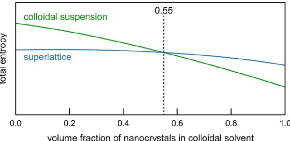
24 The self-assembly of nanocrystals into an ordered superlattice structure may seem surprising and counterintuitive at first glance. Simplifying the problem and treating all nanocrystals as a hard sphere, it is found that the phase transition is temperature-independent and therefore this is an entropically-driven process. But how can a well-ordered crystal have higher entropy than a disordered system? The answer is due to the efficiency of packing in a superlattice structure. In the superlattice geometry, each particle has more volume locally to explore and the total number of configurations possible is greater, due to the more efficient packing.20 Thus at a certain volume fraction of the nanocrystals in their solvent, approximately
55%, the entropically favored state becomes the crystalline state. This crossover, represented graphically in Figure 1.7, enables the spontaneous formation of nanocrystal superlattices.
Figure 1.6 SEM image of body-centered cubic PbS nanocrystal superlattice showing long-range ordering. Inset is the superlattice top layer – an exposed (110) close-packed plane.
From a practical standpoint, the assembly of semiconductor nanocrystals into a superlattice allows for the densest packing of nanocrystals in a film, which can lead to several beneficial properties.28 For instance,
this could be useful in nanocrystal solar cells as it decreases the film thickness required to reach a desired light absorbance. A superlattice structure also minimizes the average distance between neighboring nanocrystals, which can increase the rate of energy transfer in the film.29 As discussed earlier, there are
many different applications where PbS nanocrystals could find use. For efficient operation, these diverse applications often require very different rates of transport between neighboring nanocrystals. In photovoltaics it is desirable to maximize charge carrier extraction and transport between neighboring nanocrystals15 whereas in light conversion applications the aim is to isolate the nanocrystals from one
another, typically by embedding them in a matrix (oleic acid ligands could be useful for this application).30
Light-emitting diodes fall somewhere in between, seeking to balance charge transfer with efficient radiative recombination.13 The most readily accessible way to control the rates of transport in nanocrystal devices is
by changing how they self-assemble in order to regulate their physical distance and electronic coupling. 13,31-35 Lastly, the potential for wave-function delocalization and mini-band formation (which could greatly
enhance energy transfer in nanocrystal films) requires minimal physical disorder in a nanocrystal solid, which is most readily achieved in a self-assembled superlattice structure.15,36-39
25 Figure 1.7 Entropic relationship between the two states – colloid and superlattice – as a function of the volume fraction of nanocrystals in the solvent. The crossover around 55% volume fraction indicates when spontaneous crystallization can occur.
For these reasons, we set out to better understand the intricate process of self-assembly and how nanocrystal physical arrangement affects the optoelectronic properties of that film. Our goal was to understand how to make monodisperse PbS nanocrystals, how they self-assemble, and how this affects film performance. Overall, this contributes to the growing theme in research of controlling and directing processes at the nanoscale.
1.4 – X-ray Scattering
There are several techniques suited for the characterization of nanocrystal superlattices, such as SEM and TEM. However, these techniques are best suited for studies of local ordering, in the single micron length scale regime. Furthermore, sample thickness is constrained to a few nanocrystal layers for TEM measurements. The resolution limits of the SEM instrument is a challenge with <10 nm diameter nanocrystals as well as charging effects, which are observed in superlattices with long surface ligands.
Figure 1.8 Depiction of X-ray scattering geometry for simultaneous 2D GISAXS and GIWAXS pattern collection from a thin film of nanocrystals.
An alternative to electron microscopy is X-ray scattering, which, depending on the scattering angles measured, can probe sample features from the angstrom (atomic lattice) to nanometer (superlattice) length scales. Specifically, we have heavily relied on synchrotron-based grazing-incidence X-ray scattering
26 measurements to characterize our nanocrystal superlattices. A diagram of the grazing-incidence setup is shown in Figure 1.8. The high-flux X-ray beam impinges on the sample at a shallow angle – typically 0.25° – and the scattering patterns are collected on area detectors positioned to capture different length scales of interest. The grazing-incidence small-angle X-ray scattering (GISAXS) pattern gives information about the arrangement of the nanocrystals in their superlattice, such as the superlattice type, unit cell size, and positioning relative to the substrate. The grazing-incidence wide-angle X-ray scattering (GIWAXS) pattern gives information about the atomic lattice planes, similar to an X-ray diffraction measurement. By collecting both of these patterns simultaneously and using area detectors to collect the whole pattern, a richly detailed picture of the self-assembly is obtained. Furthermore, these measurements are indicative of a large area of the film (typically the beam width, ~50 µm, by the length of the sample, ~1cm) and can be acquired in about one second due to the high X-ray flux available at the synchrotron. For these benefits, we have found GISAXS/GIWAXS to be the most accurate and detailed characterization method for nanocrystal superlattices.
1.5 – Perovskite Nanoplatelets
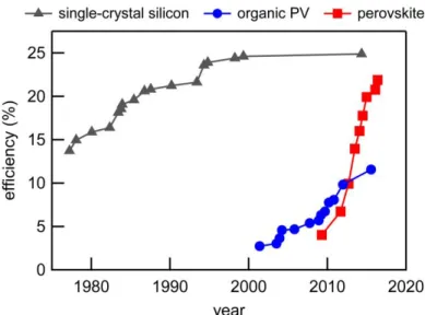
Bulk metal halide perovskite crystals have received significant attention in recent years due to their facile synthesis, long charge carrier diffusion lengths, and low trap state density.40-42 Because of these properties,
metal halide perovskites show excellent potential for LEDs, photovoltaics, and photodetectors.43-48 Most
notably, perovskite photovoltaics have seen a boom in power conversion efficiency values from 3.8% to greater than 20% in a five year time span (2009-2016).49-52 When compared with the development of other
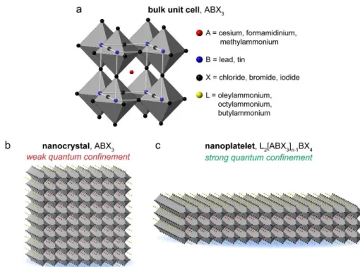
active materials, as shown in Figure 1.9, the incredible rise of perovskites becomes even more evident. The term “perovskite” describes the unit cell structure, shown in Figure 1.10a. There are many chemical constituents which can be used in this geometry. Recent work in photovoltaics and LEDs has focused on lead halide based systems.
Figure 1.9 Efficiency of photovoltaic devices over time based on active material: single-crystal silicon, organics, and perovskites. Source: NREL.
Recently, synthetic capabilities have been developed to controllably form colloidal perovskite nanocrystals and nanoplatelets. The nanocrystals are typically cubic, with side lengths of 4 nm or larger, like that depicted in Figure 1.10b.53-58 The use of long, coordinating ligands in the synthesis both controls nanocrystal
27 yields (PL QY) in the range of 50-90% and their emission can be tuned to span the visible range of the spectrum. At this size, the nanocrystals may show signs of weak quantum confinement but typically have more bulk-like absorption properties.
Figure 1.10 Representations of the different metal halide perovskite allotropes: (a) bulk perovskite unit cell and typical constituent ions, (b) cubic nanocrystal, and (c) nanoplatelet.
On the other hand, perovskite nanoplatelets can be synthesized with thicknesses less than 4 nm, such that they exhibit the effects of strong quantum confinement. By adjusting some of the synthesis conditions for nanocrystals, it is possible to confine the nanoplatelet growth in one dimension, leading to laterally large 2D nanoplatelets which are only a few unit cells thick (Figure 1.10c). As a result, the nanoplatelets show thickness-dependent absorption and emission which is blue-shifted from that of the bulk phase by ~0.6 eV. Our lab first identified and characterized these colloidal perovskite nanoplatelets in 2015 as a side product of the nanocrystal synthesis, which appeared as additional blue-shifted peaks in the absorption and emission spectra.59 As these are a recently developed colloidal semiconductor material, our focus has been
on producing homogeneous products and mapping out the properties of different atomic makeups for this flexible material system.
28
1.6 – Thesis Overview
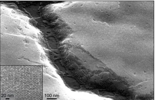
The overarching theme of this thesis is making high quality nanomaterials, understanding and controlling their assembly properties at the nanoscale, and determining how these physical properties affect the optoelectronic properties of the film. We aim to understand all the physical properties of our nanomaterials, from number of atoms which make up the individual particles to how they arrange in two and three dimensions. The stages of this process are illustrated in Figure 1.11.
Figure 1.11 Stages of self-assembly characterized by electron microscopy. (a) TEM image of a single PbS nanocrystal (b) TEM image of a 2D monolayer of PbS nanocrystals. (c) TEM image of a 3D body-centered cubic superlattice of nanocrystals. (d) SEM image of nanocrystal superlattices highlighting the extensive long-range ordering observed.
Chapter 2 focuses on how we were able to develop a synthesis for high quality PbS nanocrystals with narrow size dispersity by ensuring our reaction was diffusion-limited and not kinetically-limited. Once we were able to reliably produce these PbS nanocrystals over a wide range of diameters, we experimentally examined which parameters most affect their ability to self-assemble, using simultaneous GISAXS and GIWAXS in combination with electron microscopy. This work is detailed in Chapter 3. We then used the same approach to study how ligand exchange, which is critical for many applications, affects the nanocrystal superlattice. In Chapter 4 we present these findings and demonstrate methods for producing superlattices with compact surface ligands. We then focused our attention on the poorly-understood transition between colloidal state and superlattice state. In Chapter 5 we demonstrate that synchrotron-based X-ray scattering enables the real-time tracking of this transition with rich details that are only obtainable through this method. Finally, in Chapter 6 we present experimental evidence showing how size dispersity and resulting superlattice assembly is critical to maximizing the performance of nanocrystal films. In Chapter 7 we look at a new nanomaterial system – perovskite nanoplatelets – and use our previously developed techniques to maximize ensemble homogeneity and understand their self-assembly into stacked superstructures. We detail why these are an exciting new class of colloidal nanomaterials and demonstrate some of the first ever LEDs from these materials. Overall, this work aims to advance our understanding of processes at the nanoscale and how we can begin to direct those processes for improved performance.
29
Chapter 2 – Minimizing Size Dispersity in PbS Nanocrystals
The basis of this chapter has been published as:
M. C. Weidman, M. E. Beck, R. S. Hoffman, F. Prins, W. A. Tisdale, “Monodisperse, Air-Stable PbS Nanocrystals via Precursor Stoichiometry Control”, ACS Nano 8, 2014.
30
2.1 – Introduction
Despite the benefits offered by monodisperse nanocrystal ensembles, synthetic methods for PbS nanocrystals3,4,60 have lagged behind those for cadmium selenide (CdSe)5,61-64 and lead selenide (PbSe) 17,65-67 in terms of the monodispersity achievable over a wide range of band gap values. While the band gaps of
PbS and PbSe nanocrystals can be tuned over similar ranges, PbS offers unique advantages over PbSe in optoelectronic devices, such as improved air stability60 and the higher abundance / lower cost of sulfur as
compared to selenium.68 Furthermore, PbS is consistently the highest-performing material used in
nanocrystal solar cells.8,18,69,70
In this chapter, we show that the initial ratio of lead to sulfur precursor strongly influences the growth and monodispersity of PbS nanocrystals. For the prototypical reaction of PbCl2 with sulfur in oleylamine,3,60 we
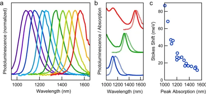
found that a large excess of lead precursor results in the formation of fewer nuclei and extends the period of growth by monomer addition from solution. In effect, this change better balances the amount of sulfur (limiting reagent) which goes towards nucleation and how much is left over for nanocrystal growth post-nucleation. By increasing the Pb:S precursor ratio to as much as 24:1, we were able to delay the onset of Ostwald ripening for up to 6 hours, making it possible to synthesize monodisperse PbS nanocrystals having peak absorption over a range of 1000–1800 nm (1.25-0.70 eV, 4.3-8.4 nm diameter) and size dispersities of 3-5%, without performing size-selective precipitations. We have also developed a new purification method such that excess lead precursor in the reaction product can be efficiently removed. Due to the unprecedented monodispersity of these nanocrystals, the half width at half max (HWHM) of the first absorption peak reaches values as small as 20 meV, suggesting an ensemble that is almost entirely homogeneously broadened. The nanocrystals have correspondingly narrow emission peaks and small Stokes shifts. The nanocrystals also exhibit exceptional air stability, as evidenced by high quantum yield and unchanging absorption spectra when stored in air for several months.
2.2 – Nanocrystal Growth Theory
The most common method for synthesizing nanocrystals is the hot-injection method, in which a solution of the chalcogenide precursor is injected into a solution of the metal precursor, with the latter typically being held at an elevated temperature. For PbS nanocrystals, elemental sulfur in a coordinating solvent (oleylamine) can be injected into lead chloride also in oleylamine to form PbS nanocrystals. The pre- and post-injection states are depicted, along with photographs, in Figure 2.1a and b. The reaction can be thought of as a phase change in which the system transitions from a supersaturated solution of precursors to below the saturation limit via the formation of nanocrystals. The classic model of nanocrystal nucleation from solution is the La Mer model.71-73
The La Mer model is graphically represented in Figure 2.1c. As the chalcogenide precursor is injected into the hot metal precursor, the concentration of precursor monomers spikes and, if concentrations are sufficiently high, causes a nucleation burst and forms the nanocrystal nuclei. The size of the initial nuclei can depend on several factors, but is notably sensitive to the temperature of the solution. The observed trend is that lower solution temperatures lead to smaller nuclei. The formation of nuclei quickly depletes the precursor concentration, such that it drops below the nucleation threshold. At this stage, no new nuclei form, however, there is still a sizeable quantity of precursors available in solution. These precursors add to the existing nanocrystals to increase their size, as larger nanocrystals are thermodynamically favorable. This is the “growth by monomer addition” regime. In this regime, if the system is well mixed, the nanocrystals will grow in a size-focusing, monodisperse fashion. This is because the monomers add at a constant rate to the nanocrystal surface, meaning that the diameter of smaller-than-average nanocrystals grows at a faster rate than the diameter of larger-than-average nanocrystals, leading to the size-focusing behavior. To
31 produce monodisperse nanocrystals over a wide range of sizes, it is desirable to make the growth by monomer addition regime (area shaded in blue) as long as possible.
Figure 2.1 Typical hot-injection synthesis scheme. (a) Separate reaction precursor solutions just prior to the injection step. (b) Reaction flask post-injection, showing an immediate color change from clear to black (indicating IR absorbing nanocrystals). (c) Stages of nanocrystal growth as a function of time and precursor concentration, according to the LaMer growth mechanism.
Once the precursor concentration is depleted, the nanocrystals continue to grow but in a dispersity-increasing fashion called Ostwald ripening. In the Ostwald ripening regime, the nanocrystals progress towards thermodynamically-favored larger crystals but by dissolution of smaller nanocrystals or the combination of nanocrystals. To produce monodisperse nanocrystals, this regime should be avoided.
2.2 – Quantifying Size Dispersity
To determine the effect of Pb:S precursor ratio on nanocrystal growth, PbS nanocrystals were synthesized at 120°C with Pb:S precursor ratios of 4:1, 8:1, and 24:1. After injection of the sulfur solution into the lead solution, growth was allowed to occur at 120°C for several hours. During this time, the nanocrystals increased in size and the first absorption peak shifted to longer wavelengths. In this work, we use the HWHM of the first absorption peak as a metric for the size dispersity of the nanocrystals, with a small HWHM value signaling a monodisperse batch of nanocrystals. The HWHM is determined from the peak absorption to the half max value at longer wavelength (i.e. to the right of the first absorption peaks shown in Figure 2.2).
32 Figure 2.2 Comparison of absorption spectra and TEM micrographs for nanocrystals having the same peak absorption wavelength but different HWHM values.
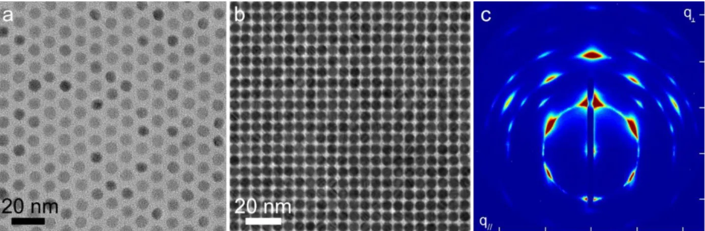
To illustrate that HWHM is a reliable metric for dispersity, we compare in Figure 2.2 the absorption spectra of nanocrystals synthesized with the same first absorption peak location, but different peak HWHM values. The spectrum shown in red has a HWHM of 42 meV while the blue spectrum has a HWHM of only 25 meV. We can identify five absorption features in the blue spectrum (determined by taking the second derivative of the data, not shown), whereas only two absorption features are observed in the red spectrum. The transmission electron microscopy (TEM) images of these samples confirm the improved monodispersity of the 25 meV HWHM sample over the 42 meV sample, as well as the ability to self-assemble, which is lacking in the 42 meV sample.
In Figure 2.3, we plot the HWHM for nanocrystals synthesized with varying Pb:S precursor ratios as a function of their peak absorption wavelength. We include the smallest HWHM values obtained for at least two syntheses at each precursor ratio studied. The dashed gray line is the expected trend for a nanocrystal dispersion having 3.3% size dispersity (see further discussion below on this calculation). For a 4:1 precursor ratio, the HWHM followed the line of constant monodispersity until growth reached a peak wavelength value near 1400 nm, at which point HWHM began to increase rapidly. With an 8:1 Pb:S ratio, the monodisperse growth occurred until about 1600 nm, at which point HWHM started to increase with increasing absorption wavelength. For a ratio of 24:1, the monodisperse growth proceeded up to 1800 nm, and reached values as low as 20 meV. Interestingly, a precursor ratio of 24:3 resulted in a growth curve similar to 8:1, indicating that it is precursor ratio – rather than total precursor concentration – that enables monodisperse growth. Elemental analysis by energy-dispersive X-ray spectroscopy (EDS) confirmed previous reports that PbS nanocrystals prepared by this reaction are lead-rich.3,60 A comparison between
the similarly sized nanocrystals shown in Figure 2.2, synthesized using 4:1 and 24:1 Pb:S ratios, revealed no statistically significant difference in their elemental composition.