HAL Id: hal-03092482
https://hal.archives-ouvertes.fr/hal-03092482
Submitted on 5 Jan 2021
HAL is a multi-disciplinary open access
archive for the deposit and dissemination of
sci-entific research documents, whether they are
pub-lished or not. The documents may come from
teaching and research institutions in France or
abroad, or from public or private research centers.
L’archive ouverte pluridisciplinaire HAL, est
destinée au dépôt et à la diffusion de documents
scientifiques de niveau recherche, publiés ou non,
émanant des établissements d’enseignement et de
recherche français ou étrangers, des laboratoires
publics ou privés.
Reliable method for accurate measurements of the
breakdown voltage in microgaps
Aditya Purba, Antoine Belinger, Jean-Pascal Cambronne, Ngapuli Sinisuka, K
Makasheva
To cite this version:
Aditya Purba, Antoine Belinger, Jean-Pascal Cambronne, Ngapuli Sinisuka, K Makasheva. Reliable
method for accurate measurements of the breakdown voltage in microgaps. IEEE Conference on
Electrical Insulation and Dielectric Phenomena (IEEE CEIDP 2020), Oct 2020, East Rutherford,
United States. �hal-03092482�
Reliable method for accurate measurements
of the breakdown voltage in microgaps
Aditya Eka Purba Sejati LAPLACE, Université de Toulouse,
CNRS, UPS, INPT Toulouse, France Bandung Institute of Technology
Bandung, Indonesia PT. PLN Persero Jakarta, Indonesia purba.aditya@yahoo.com
Ngapuli I. Sinisuka Bandung Institute of Technology
Bandung, Indonesia n.irmea@gmail.com
Jean-Pascal Cambronne LAPLACE, Université de Toulouse,
CNRS, UPS, INPT Toulouse, France cambronne@laplace.univ-tlse.fr
Kremena Makasheva LAPLACE, Université de Toulouse,
CNRS, UPS, INPT Toulouse, France makasheva@laplace.univ-tlse.fr
Antoine Belinger LAPLACE, Université de Toulouse,
CNRS, UPS, INPT Toulouse, France belinger@laplace.univ-tlse.fr
Abstract— The up-to-date tendency of compact design of low/medium voltage equipment implies micrometer distances between the active parts. In order to reduce losses and prevent operational failure of the devices under such conditions, knowledge on the breakdown voltage is essential. However, measurements of the breakdown voltage in microgaps remains quite delicate experiment, mainly because of difficulties related to the accurate definition of the distance between the electrodes. To overcome these limitations, we propose here a reliable method based on measurements of the current amplitude and phase between current and applied voltage for AC signals. It is shown that when contact between the two electrodes occurs the current amplitude increases substantially and the phase changes abruptly to zero. Thus, no arbitrary conditions are needed to define the contact point. The system is well-defined and the procedure accuracy improved.
I. INTRODUCTION
Due to the fast development of massive technology solutions, microelectronic industry and nanotechnology products increase very rapidly in numbers and varieties. The era of migration towards smaller dimensions of the outcome devices presents new challenges related among others to the reliability of the equipment. To meet these challenges, an in-depth understanding of the equipment failure on the physical side is required, so that the long-term reliability of products or processes can be evaluated. Accordingly, many research groups renewed their interest to the study of electrical breakdown phenomena in micro- and even nano-gaps [1-9].
Electrical breakdown in gases is well described by the Paschen’s law that uniquely relates the breakdown voltage with the pressure times distance (p × d) product. Contrary to the case of large scale electrode separations, the experiments performed in microgaps (< 10 µm) at atmospheric pressure show much lower breakdown voltages than the ones predicted by the Paschen’s law [1-4, 6-8]. When reducing the inter-electrode distance, mechanisms like field electron emission start playing
role in the electron yield in addition to the secondary electron emission and the ionization in the gas, leading to lower breakdown voltages. In general, the electrical breakdown is defined by the combined effect of a large number of parameters: nature of the gas, pressure, inter-electrode distance, geometry of the electrodes, cathode material, and in particular its work function, surface roughness, protrusions, ambient temperature,
etc. For microgaps the above parameters may present instable
features due to gradient variations and interdependence, and thus make the analysis of the underlying mechanisms more difficult. Therefore, to reach a better understanding of the phenomena at play a reliable method for measurements of the breakdown voltage in micrometer gaps is essential.
The breakdown voltage criterion is often chosen to be the presence of measurable current (in the order of a few milliamps) in the circuit after applying voltage from the power supply [1-4, 7, 8]. Critical step in the breakdown voltage measurement procedure in microgaps is defining the contact point between the two electrodes. Once the contact point is found, one of the electrodes is stepped back to precisely define the inter-electrode distance. According to the reported in the literature studies there are different protocols for determining the contact point, particularly in tip-to-plane electrode configuration: (i) observation under optical microscope until achieving mechanical contact between the electrodes [7]. This procedure is acceptable in the general case, but does not consider any electrical properties of the environment. It might lead to a large uncertainty in the breakdown voltage value that is attributed to a given inter-electrode distance, especially for very small microgaps; (ii) more reliable criterion is obtaining electrical contact between the two electrodes [1-4, 7, 8]. To reach contact, the tip-electrode is slowly approached to the plane and the contact point is defined when measurable current is detected in the circuit after applying a DC bias of 1-2 V. This criterion meets all required conditions, but registering gradually increasing currents in the order of 1 nA might be delicate.
To precisely define the contact point our strategy relies on using the threshold behavior of some characteristics of the current and voltage waveforms by using AC signals. In this paper we focus on description of the performed experiments and the simulation approach that has been applied for development of the method for accurate measurements of breakdown voltages in microgaps. Control of the contact point, hence the inter-electrode distance, certainly adds value to the precise description of breakdown phenomena in microgaps.
II. EXPERIMENTAL SETUP, SIMULATION APPROACH AND
MEASUREMENT PROCEDURE
A. Schematic Design and Apparatus
The electrode configuration is tip-to-plane; the tip electrode is a tungsten needle with well controlled radius (Rc = 10 µm)
facing an Au-metallized plate (Fig. 1). This experimental set-up is an improved version of a previously developed system in LAPLACE [9, 10]. The needle is connected to a voltage source through a 142 kΩ series resistance (Rm) and the plate electrode
is grounded. An AC signal (0.1 – 10 MHz, 10 V) is applied to the needle for the contact point definition. Then the breakdown voltage is measured for 1 – 10 µm gaps at atmospheric pressure and room temperature. To that end the tip is connected to a Keithley 2410 DC voltage source supplying voltages up to 1100 V. The current is detected using a Tektronix CT-1 with P6041 current probe (5 mV/mA) connected to a Wavesurfer 3024 oscilloscope.
Fig. 1. Schematic design of experimental set-up.
The position of the plane (cathode) electrode can be adjusted manually through a x-y linear stage. The tip (anode) electrode settings are made in x-axis by using a micro positioner: piezo-actuator, PI Hera 621.UD with E.709-CRG controller, connected to a PC. The piezo-electric actuator enables control of the distance between the two electrodes with accuracy of ± 10 nm. To obtain this high precision the electrodes are placed on a marble plate. Observation of the tip-to-plane electrode configuration is performed by using a Keyence VHX-1000 digital microscope.
B. Simulation approach to consider effects induced by protrusions on the equivalent capacitance in the gap
As mentioned above irregularities on the electrode surface (roughness, protrusions) modify the breakdown voltage for a
given electrode configuration due to a strong enhancement of the electrical field in the gap [9, 10].
Fig. 2. The simulated electrode configuration without protrusion in (a) and with protrusions in (b).
To account for effects induced by protrusions on the equivalent capacitance variation in the gap we have performed numerical simulations by using the FEMM software (Ver.4.2). The simulation applies finite element modeling (FEM) to extract the equivalent capacitance in the gap as function of the inter-electrode distance and compare it to the one in presence of protrusions on the electrode surface. Basically, the concept of FEM analysis involves four steps, namely discretizing the solution area into a number of sub-regions or finite elements, then obtaining an equation for a typical element followed by assembling all the elements in the solution region, and the last step is solving the system of the obtained equations [11]. The considered in the simulation tip-to-plane electrode configuration is shown in Fig. 2(a). The surface irregularities are considered by an isosceles triangle protrusion with a maximum height of 10 nm (comparable to the measured by profilometry highest peak on the Au-metalized plate electrode, results not shown here) placed on the surface of the plane electrode in front of the tip, as illustrated in Fig. 2(b). Such configuration represents the worst scenario. The other parameters involved in the FEM simulation are: needle (tip) electrode made of tungsten with radius Rc = 1 μm and length of
50 μm, and gap between the electrodes varied in the range 10 – 200 nm. The applied on the tip (anode) voltage is Vanode = 300 V, while the plane electrode is grounded
(Vcathode = 0 V).
C. Procedure for measurement of contact between electrodes
The measurement procedure, applied to define contact between the electrodes, follows two protocols for accuracy. The first protocol concerns the needle approach to the plate at nanometer scale (flowchart is shown in Fig. 3). The needle electrode is moved in small steps by using the piezo-actuator. In non-contact conditions, current flow occurs with significant phase difference with respect to the input source. When the contact point is achieved (d = 0) the phase difference between the input source and the output current becomes close to zero. The second protocol is performed after each step of the first one. It consists in a simple measurement of the current amplitude. The contact occurs when the current amplitude increases drastically. Thus the contact point between the two electrodes is defined when both protocols are validated.
Pack Anode Piezo-actuator Additional Support
Base Support
a axe unique – centre Metrique 32 mm
S
142 kΩ
A
+
-Gap
Voltage Source Amp meter
Oscilloscope Camera/Microscope Keyence
Fig. 3. Flowchart of the procedure to define contact point between needle and plate electrodes (d = 0 position).
III. RESULTS AND DISCUSSION
The developed method is presented for a frequency of 0.2 MHz and applied voltage of 10 V between the electrodes (Fig. 4). The variation of the current amplitude and phase is followed when the tip-electrode approaches the plane-electrode until contact. We note hereafter the amplitude of current with contact IC and without contact INC, respectively. We also define
the phase between the voltage and the current when the electrodes are not in contact by NC and the phase when the
electrodes are in contact by C.
Fig. 4. Current and voltage waveforms. Applied voltage 10V (black curve) in both cases. In blue, the current when the electrodes are not in contact. In red,
the current when contact occurs.
As can be observed on Fig. 4, the current amplitude doubles and the phase is greatly reduced when the electrodes are in contact compared to the no contact conditions. When the electrodes are not in contact, the current is limited by the
equivalent capacitance due to the gap (Cg) between the
electrodes and the resistance of measurement (Rm) as presented
in Fig. 5. Basically, when the contact occurs there is no gap. The capacitance is short circuited and the current is only limited by the resistance. Therefore, the phase C is close to zero and
the current IC increases.
Fig. 5. Equivalent circuit of the system: Rm is the measurement resistance,
Cg is the equivalent capacitance of the gap.
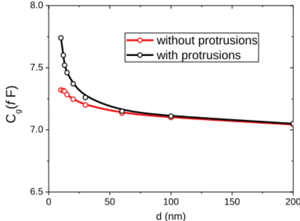
The gap capacitance is the main difference between the measurement with contact and without contact. However, it is very difficult to estimate experimentally the value of this capacitance from the current and voltage measurements. Indeed, a very small error on the estimation of a parasitic impedance (as the wire inductance) affects strongly the value of the capacitance. In consequence, we have calculated this capacitance by simulation, as shown in Fig. 6. The obtained results show that the Cg-value is not significantly affected by the inter-electrode
distance (d) or by the presence of protrusions on the electrode surface. The Cg-value remains between 7 and 8 femto Farad. As
long as there is no contact, the displacement of the electrode does not affect the equivalent circuit (Rm and Cg). This explains as why
experimentally the current (INC and NC) is not modified by the
gap d as long as there is no contact between the electrodes. It also strengthens the reliability level of the method because modification on the current (phase and amplitude) can only occur due to contact between the electrodes.
Fig. 6. Comparison of the equivalent capacitance values against inter-electrode gaps with and without protrusions based on the simulation results.
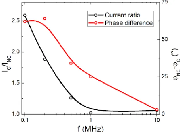
The method, that we propose here, to detect the contact is accurate as long as the impedance of the capacitance is higher or equivalent to the resistance. As defined by the two protocols presented above, there are two conditions to fulfil in order to get high accuracy: the current amplitude ratio IC/INC and the
current phase difference NC – C should be large. In addition,
the change of the current phase occurs suddenly when the contact condition is achieved. Fig. 7 shows the frequency range
START
Move the piezo actuator slowly (incremental -> 10 nm)
Finish Yes No
Applied Voltage –> 10 V (phase angle between Input voltage and
Output current is far from zero)
Define as contact (d = 0) Default adjustment: no contact
between needle and plate electrodes
Phase angle monitored on oscilloscope
close to zero?
When contact occurs
Cg Rm 0 50 100 150 200 6.5 7.0 7.5 8.0 Cg (f F) d (nm) without protrusions with protrusions
of applicability of the method. For frequencies below 0.1 MHz, the current amplitude is not significant to be measured with accuracy and the method cannot be applied. For 1 MHz the current amplitude ratio IC/INC is close to 1, as shown in Fig. 7.
There is no difference in the current amplitude, yet the phase difference is still up to 25°. For frequencies above 1 MHz, the current phase difference NC – C is close to zero because the
value of the capacitance impedance is quite low compared to the series resistance. Therefore, in our configuration, this method is practical for applied frequencies in the range 0.1 MHz - 1 MHz.
Fig. 7. Evolution with the frequency of the current ratio (black) and the phase difference (red). The current ratio is defined as IC/INC. The current phase
difference is defined as NC-C.
The developed in this work method allows to position accurately the needle against the plate electrode, i.e. the corresponding breakdown voltage can accurately be attributed to the inter-electrode distance. The uncertainty in the inter-electrode distance is defined only by the piezo-actuator. Compared to the other methods described earlier, the double information acquired here (phase shift and growth of the current amplitude) ensures the accuracy of the contact. Moreover, the conditions for contact are not arbitrary. They are imposed by the system. Then the step back of the needle electrode with the piezo-electric actuator defines exactly the inter-electrode distance d.
Fig. 8. Breakdown voltage versus the inter-electrode distance in air at atmospheric pressure and room temperature.
Application of the method is demonstrated in Fig. 8. A continuous voltage is applied and the breakdown voltage (VB)
is determined for different inter-electrode distances in the range 1 – 10 µm. The three characteristic regions for microgaps are clearly observable: the classical curve of breakdown voltage following the Paschen law (for gaps higher than 9 µm), the plateau (between 5.5 and 9 µm) and the deviation from Paschen region (for gaps below 5.5 µm).
IV. CONCLUSION
The method developed in this work allows accurate measurements of the breakdown voltage in microgaps. It relies on the threshold behavior of some characteristics of the current and voltage waveforms by using AC signals to define contact between the two electrodes. Two conditions are required to be fulfilled in order to get high accuracy: the current amplitude ratio IC/INC and the current phase difference NC – C should be
large. Thus the criterion for contact between the electrodes is not arbitrary. It is entirely imposed by the system. Future work will be directed to systematic studies of the breakdown voltage in microgaps as function of the gas nature, pressure, cathode material, surface roughness, and other relevant factors.
REFERENCES
[1] J.-M. Torres and R. S. Dhariwal, “Electric field breakdown at micrometer separations,” Nanotechnology, vol. 10, pp. 102-107, 1999.
[2] P. G. Slade and E. D. Taylor, “Electrical breakdown in atmospheric air between closely spaced (0.2μm-40 μm) electrical contacts,” IEEE Trans. Components Packag. Technol., vol. 25, no. 3, pp. 390–396, 2002.
[3] M. Klas and Š. Matejčík, “DC breakdown in air, oxygen and nitrogen at micrometer separations,” HAKONE 2010 - 12th Int. Symp. High Press. Low Temp. Plasma Chem., vol. 2, pp. 112–116, 2010.
[4] A. Peschot, N. Bonifaci, O. Lesaint, C. Valadares, and C. Poulain, “Deviations from the Paschen’s law at short gap distances from 100 nm to 10 μm in air and nitrogen,” Appl. Phys. Lett., vol. 105, p. 123109, 2014. [5] K. Makasheva, C. Villeneuve-Faure, C. Laurent, B. Despax, L. Boudou,
and G. Teyssedre “Dielectric charging by AFM in tip-to-sample space mode: overview and challenges in revealing the appropriate mechanisms,” Nanotechnology, vol. 26, p. 295704, 2015.
[6] D. B. Go and A. Venkattraman, “Microscale gas breakdown: ion-enhanced field emission and the modified Paschen’s curve,” J. Phys. Appl. Phys., vol. 47, no. 50, p. 503001, 2014.
[7] G. T. Anuraga, J.-P. Cambronne, S. Dinculescu, N. I. Sinisuka, and K. Makasheva, “A Contribution to Breakdown Voltage Characteristics in Air for Inter-electrode Distances 1 - 10 μm at Various Pressures,” Book Series:
IEEE Nanotechnology Materials and Devices Conference (IEEE NMDC 2016), vol. 1, pp. 44-45, 2016.
[8] K. Tofani, J.-P. Cambronne, S. Dinculescu, N. I. Sinisuka, and K. Makasheva, “Methodology for analysis of electrical breakdown in micrometer gaps in tip-to-plane configuration,” Book series: IEEE
Nanotechnology Materials and Devices Conference (IEEE NMDC 2018),
vol. 1, pp. 1-4, 2018.
[9] Fathur Rahman, Jean-Pascal Cambronne, Antoine Belinger, Ngapuli I. Sinisuka, and Kremena Makasheva, “Electric Field Enhancement Factor defined by nanoprotrusions on the electrode surface in microgaps in needle-plate configuration,” 14th IEEE Nanotechnology Materials and
Devices Conference (IEEE NMDC 2019), October 27–30, 2019,
Stockholm, Sweden.
[10] Y. Fu, P. Zhang and J.P. Verboncoeur, "Pashen's curve in microgaps with an electrode surface protrusion", Appl. Phys. Lett., vol 113, p. 054102, 2018. [11] M. N. O. Sadiku, “A Simple Introduction to Finite Element Analysis of
Electromagnetic Problems,” IEEE Trans. Educ., vol. 32, no. 2, pp. 85–93, 1989.