.
Design and Implementation of a Preload
MASSACHUSETTS INSTITUTE
Electronics Architecture for
a MEMS
OF TECHNOLOGYAccelerometer
OCT 0
4 2010
by
..
LIBRARIES
Alvin Lai Lin
Submitted to the Department of Electrical Engineering and Computer
Science
in partial fulfillment of the requirements for the degree of
Master of Engineering in Electrical Engineering and Computer Science
at the
MASSACHUSETTS INSTITUTE OF TECHNOLOGY
ARCHIVES
February 2006
@ Alvin Lai Lin, MMVI. All rights reserved.
The author hereby grants to MIT permission to reproduce and
distribute publicly paper and electronic copies of this thesis document
in whole or in part.
A uthor ... . .... .. ... ...
Department of Electrical Engineering and Computer Science
r
February 3, 2006
Certified by...
....
.. .. ... .David J. McGorty
Principal Member Technical Staff, C.S. Draper Laboratory
Thesis Supervisor
Certified by...
...
i
bJeffrey
H. Lang
w1 -~ ProfessorThesis Advisor
Accepted by...
Arthur C. Smith
Design and Implementation of a Preload Electronics
Architecture for a MEMS Accelerometer
by
Alvin Lai Lin
Submitted to the Department of Electrical Engineering and Computer Science on February 3, 2006, in partial fulfillment of the
requirements for the degree of
Master of Engineering in Electrical Engineering and Computer Science
Abstract
This thesis describes the design and implementation of an electronics system to provide rebalancing and readout for a force-rebalanced microelectromechanical ac-celerometer. A feedback control loop is devised using a novel preload architecture, compensating the proof mass of the sensor and providing an accurate acceleration measurement. This architecture is compared to alternative methods of linearizing the control loop. The electronics system is divided into analog and digital subsystems. The design is analyzed at several abstraction levels. The system is implemented for prototype testing with discrete components on a printed circuit board with a MEMS sensor attached. A computer program is implemented to receive and process the readout data using the serial port.
The design methodology consists of a top-down design flow based on simulation. At each iteration in the design process, the lower level abstraction is verified with the previous model. Eventually, the design reaches the level of synthesizable digital logic and discrete analog components. This thesis describes the design process and implementation details for creating an accelerometer system prototype ready for lab testing. Detailed simulations indicate that the implemented design is likely to meet the design goals for a personal navigation system suitable for a human or land vehicle. Conclusions on design methodology and verification techniques are also presented.
Technical Supervisor: David J. McGorty
Title: Principal Member Technical Staff, C.S. Draper Laboratory
Thesis Advisor: Jeffrey H. Lang Title: Professor
Acknowledgments
I would like to thank my thesis supervisors, Dave McGorty and Professor Jeff
Lang for their guidance and support during this research. In addition, this work would not have been possible without the tremendous contributions of my friends and colleagues at Draper Laboratory, especially Richard Elliott and John LaChapelle. I am extremely grateful for their assistance throughout the course of my resesarch..
This thesis was prepared at The Charles Stark Draper Laboratory, Inc., under Contract B54530612 / 4200047939, sponsored by Honeywell International Inc., Min-neapolis, Minnesota.
Publication of this thesis does not constitute approval by Draper or the sponsoring agency of the findings or conclusions contained herein. It is published for the exchange and stimulation of ideas.
Permission is hereby granted to the Massachusetts Institute of Technology to reproduce any or all of this thesis.
Contents
1 Introduction
15
1.1 O verview .. . . . . . . . . 15 1.2 Design Methodology... . . . . . . . . . .. 16 1.3 Research Objective... . . . . . . .. 18 1.4 T hesis O utline . . . . 18 2 System Overview 19 2.1 Sensor Characteristics ... . . . .. 202.1.1 Ideal Sensor Model & Behavior . . . . 20
2.1.2 Physical Sensor Details & Consequences . . . . 26
2.1.3 Modeling the MEMS Sensor . . . . 27
2.2 Electronics Requirements... . . . .. 28
2.3 Architecture Design... . . . . . . . . 28
2.3.1 Preload Architecture Concept . . . . 29
2.3.2 Alternative Architecture... . . .. 31
2.4 Analog & Digital Subsystems . . . . 32
2.5 Frequency and Sample Rate Selection . . . . 34
2.6 Functional Simulation... . . . . . . .. 36
3 Digital Design
39
3.1 D igital Overview . . . . 393.2 Demodulator. . ... . . . .. 41
3.4 PI Controller...
. . . .
. . . .
48
3.5 CIC Interpolation Filter.. . . .
. . . .
50
3.6 Torque Adjustment Module . . . .
52
3.7 D/A Sigma-Delta Modulator.... . . .
. . . ..
53
3.7.1
Coefficient Generation . . . .
54
3.7.2
Output Density of Ones Scaling . . . .
57
3.8
Output Transmitter . . . .
58
3.8.1
Acceleration Output CIC Decimation Filter..
. . . ..
59
3.8.2
Compensation Variable CIC Decimation Filter . . . .
60
3.8.3
UART.. . . .
. . . .
61
3.9 Synthesis Results... . . . .
. . . .
64
4 Analog Design
67
4.1 Analog Overview . . . .
67
4.2 Level Shifter . . . .
69
4.3 Low Pass Filter . . . .
71
4.4 Torque Commutator . . . .
73
4.5 Slew-Rate Limiter... . . . .
. . . .
75
5 Implementation Details
79
5.1
Coefficient Scaling
. . . .
79
5.2 ASIC & PC Interfacing
. . . ..
81
5.3 Software Design . . . .
82
5.4 Component Selection... . . . .
. . . .
84
5.4.1
Analog Multiplexer.. . . . .
. . . .
84
5.4.2
ASIC Interface Level Shifters . . . .
85
5.4.3
FPGA.. . . .
. . . .
85
5.4.4
O p-A m ps . . . .
86
5.4.5
Torque Channel Level Shifter . . . .
86
5.5
Printed Circuit Board Layout . . . .
86
5.5.1
Layer Stackup . . . .
87
5.5.2 Sensor Placement . . . . 90
5.5.3 Bypass/Decoupling Capacitors... . . . . .. 90
5.5.4 Sym m etry . . . . 91
List of Figures
1-1
Top-down Design Methodology
. . . .
2-1 High Level Block Diagram of Accelerometer System . . . . .
2-2 Physical Diagram of MEMS Accelerometer .
...
2-3 Ideal Characterization of Sensor Scale Factor . . . .
2-4 Ideal Characterization of Sensor Torque Constant . . . .
2-5 Example Scheme to Rebalance Sensor Using DC Torquing
2-6 Finite Slew Rate Effects on Torque Voltage . . . .
2-7 Preload Scheme to Rebalance Sensor . . . .
2-8 Preload Architecture Electronics Overview....
. . . ...
2-9 Frequency Spectrum of Ideal 20KHz Square Wave . . . .
2-10 Functional Model Setup for Preload Architecture
. . . .
2-11 Functional Model Simulation Results... . . . .
3-1
3-2
3-3
3-4
3-5
3-6
3-7
3-8
3-9
3-10
Digital Subsystem Block Diagram . . . .
40
Optimized Sine Storage for Demodulator ROM
. . . .
42
Demodulator Multiplexer to Eliminate Multiplications
. . . .
43
Integrator Stage for CIC Filter . . . .
44
Comb Stage for CIC Filter . . . .
44
Frequency Response for CIC Decimation Filter . . . .
45
Block Diagram for CIC Decimation Filter... . . . .
. . .
47
Simulation Model for PI Controller...
. . . . .
. . . .
48
System Step Response for Properly Tuned K, and Ki
. . . ..
49
Block Diagram for CIC Interpolation Filter . .
Noise Transfer Function Magnitude Response
M odulator . . . .
Standard Form for Sigma-Delta Modulator . .
Component of Output Transmitter . . . .
Example UART Packet . . . .
Order of Transmitted Output Data Packets
Output Transmitter Finite State Machine
3-11
3-12
3-13
3-14
3-15
3-16
3-17
4-1
4-2
4-3
4-4
4-5
4-6
4-7
4-8
4-9
4-10
5-1
5-2
5-3
5-4
5-5
5-6
5-7
Digital Torque Magnitudes in Response to a
+10g
Step Input
Screenshot of Data Capturing Java Application . . . .
Layer Stackup for PCB . . . .
Power Plane in PCB.
. . . .
.
Sensor Placement and Signal Integrity Protection . . . .
Bypass Capacitor Placement for the MAX3221 . . . .
Bypass Capacitor Placement for the FPGA . . . .
.
81
.
83
.
87
.
89
.
89
.
90
.
91
. . . .
for D/A Sigma-Delta
.
. . . .
55
. . . .
55
. . . .
58
. . . .
61
. . . .
62
. . . .
64
Abstract Analog Subsystem Block Diagram . . . .
Detailed Analog Subsystem Block Diagram . . . .
Power Spectrum for Sigma-Delta Modulator Output . . . .
Zoomed Power Spectrum for Sigma-Delta Modulator Output . . . . .
Analog Subsystem Active 4th Order Sallen-Key Butterworth Low Pass
F ilter C ircuit . . . .
Analog Subsystem Low Pass Filter Magnitude Response . . . .
Power Spectrum of Analog Subsystem Low Pass Filtered Output
.
. .
Inverter C ircuit . . . .
Slew-Rate Limiter Circuit: First Order Sallen-Key Butterworth Filter
Slew-Rate Limited Torque Signal . . . .
List of Tables
1.1 Design Goals for Accelerometer Electronics . . . . 16
2.1 Typical Sensor Characteristics . . . . 23
2.2 Nominal Voltages for Preload Architecture... . . . . . . ... 30
2.3 Nominal Frequencies and Sample Rates for Preload Architecture . . . 34
3.1 CIC Decimation Filter Parameters... . . . . . . . . . 43
3.2 CIC Decimation Filter Attenuation at Selected Frequencies . . . . 46
3.3 Register Sizes for CIC Decimation Filter . . . . 47
3.4 Tuned Ki and K, From Step Response of Detailed Simulation . . . . 49
3.5 CIC Interpolation Filter Parameters... . . . . . . . . 51
3.6 Register Sizes for CIC Interpolation Filter... . . . . . . .. . 51
3.7 Density of Ones for Sigma-Delta Modulated Outputs. . . . . ... 53
3.8 Parameters for D/A Sigma-Delta Modulator . . . . 54
3.9 State Space Coefficients for Sigma-Delta Modulator... . . . . . . 56
3.10 Feedback Values for Sigma-Delta Modulator... .. . 57
3.11 Acceleration Output CIC Decimation Filter Parameters.. . . ... 59
3.12 Register Sizes for Acceleration Output CIC Decimation Filter . . . . 60
3.13 Compensation Variable CIC Decimation Filter Parameters . . . . 60
3.14 Register Sizes for Compensation Variable CIC Decimation Filter . . . 61
3.15 Synthesis Sizes for Digital Blocks . . . . 64
3.16 Percent of Total Synthesis Size for Digital Blocks... . . . . . . 65
4.2 Level Shifter Signal Representations . . . .
70
4.3 Example Scheme to Create Out-of-Phase Commutated Torque Signals
75
5.1
Components Chosen for the Prototype Board . . . .
84
5.2 Percentage Utilization of the FPGA . . . .
85
5.3 Voltage Levels, Functions, and Presence on Power Plane of Voltage
Chapter 1
Introduction
1.1
Overview
The development of microelectromechanical systems (MEMS) has unlocked a spec-trum of applications which are uniquely leveraged by these systems. MEMS systems contain electronic components as well as micromachined mechanical components and are able to provide sensing, mechanical action and computation capabilities on one integrated circuit [10]. Such a MEMS system is capable of better performance and longer operational lifetime than the corresponding macroscopic system. For these reasons, the Charles Stark Draper Laboratory has been developing high performance inertial sensors using M\JEMS technology. These sensors typically consist of single axis accelerometers or plane rotation gyroscopes.
Single axis accelerometers are useful for many applications involving navigation or movement. The acceleration measurement can be used to prevent a vehicle or person from being operated in a manner that exceeds its safety boundaries or structural integrity limits. The acceleration can also be integrated over time to provide a velocity estimate. This velocity estimate is useful for navigation purposes; it can be integrated over time to provide a position estimate. Using MEMS technology to implement accelerometers allows for a small package size and a durable and reliable system. In addition, several accelerometers can be packaged together to allow for an integrated three axis solution.
Characteristic
Target Specification
Input Range ±10g Input Bandwidth 0Hz to 100Hz Input Attenuation >-3dB
Table 1.1: Design Goals for Accelerometer Electronics
The MEMS accelerometer is a passive sensor that consists of micromachined me-chanical parts that can be stimulated with electrical signals [10]. An electronics system is required to read, filter, and process the signals coming out of the sensor as well as provide the necessary signals going into the sensor [28]. This thesis describes the design and implementation of such an electronics system. The electronics system uses a novel approach that has not been used before in the design of accelerometer electronics. Thus, there are no stringent specifications placed on the performance of the final system. Rather, there are several design goals set with the intention of providing a framework from which performance can then be measured and compared to alternative systems. These design goals are outlined in Table 1.1. They are the specifications necessary (without precision requirements) for a personal navigation accelerometer.
1.2
Design Methodology
The design methodology consists of a hierarchical approach with a heavy emphasis on simulation. Recent advances in computer simulation technology allow the system to be represented from an ideal mathematical model all the way down to register transfer level (RTL) logic for the digital subsystem. Confirmation of a working system at all levels of abstraction ensure that the design works as intended and will have minimal unexpected effects after implementation and fabrication.
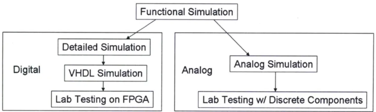
The first modeling and simulations are run at the highest possible level, with subsequent simulations adding detail by replacing high level blocks with more detailed blocks. This is commonly referred to as a top-down design process [23]. As the blocks gain detail, they more closely resemble the real world components which they
Functional Simulation
Detailed Simulation
Digital
VHDL Simulation
Analog
Analog Simulation
Lab Testing on FPGA
Lab Testing w/ Discrete Components
Figure 1-1: Top-down Design Methodology
represent. The design is complete when the blocks are as detailed as possible can
no longer be replaced with more exact models. At this point, the design is ready to
translate into real world electronic components for final testing.
Figure 1-1 illustrates the top-down design methodology for the entire electronics
system. In the first step, the entire system is simulated at a functional level. As
each simulation at a given abstraction level runs satisfactorily, the design process can
continue by following the arrows down the chain. After the functional simulation,
the first digital simulation is a detailed version of the digital components. In this
detailed model, all digital signal processing structures are intact in their architecture,
but they .are not detailed to the point where registers and transistors are defined.
Next, VHDL is used to describe the digital hardware and the simulation results of
this hardware are compared to the detailed simulation results. The only difference
between the detailed simulation and the VHDL simulation should be the differing
levels of quantization found in the two simulations. The final testing phase for the
digital electronics system is to synthesize the digital logic onto an FPGA for lab
testing. This is the most convenient way to run an test with an actual MEMS sensor
rather than a model.
The analog design methodology is also shown in Figure 1-1 and is different than
the digital design methodology. The functional simulation can lead directly into an
analog simulation of the design, bypassing the detailed simulation found in the digital
design flow. A detailed simulation is not necessary because the functional simulation
can translate well into the analog design and simulation without an intermediate step. After the analog simulation is verified, lab testing can be performed to verify that the analog components match the analog simulation.
1.3
Research Objective
The objective of this thesis is to design and implement an electronics design for a force rebalanced MEMS accelerometer using the preload architecture. Since the preload architecture has never been implemented, the design requires a development of the entire electronic system. The design process is clearly described and documented, with all significant design decisions explained. The final product is a working MEMS accelerometer system on a test board, capable of accurately measuring acceleration within the limits described in Table 1.1.
1.4
Thesis Outline
The remainder of this thesis is organized as follows. Chapter 2 provides a high level system overview of the accelerometer electronics system, as well as a detailed description of the MEMS sensor. Chapter 3 presents the design of the digital logic. Chapter 4 presents the design of the analog circuitry. Chapter 5 describes the software design as well as other implementation details such as part selection and printed circuit board (PCB) layout. Chapter 6 details some final conclusions and makes suggestions for future work.
Chapter 2
System Overview
In this chapter, the overall system is described. The MEMS sensor is explained and characterized in detail. Next, the electronics requirements for the system are given. After this, the preload architecture is presented, which provides insight on how the system is organized. Alternative architectures are also discussed along with several key advantages and disadvantages of each alternative. Finally, the an overviews of the analog and digital subsystems are presented with an explanation on the separation of the two domains.
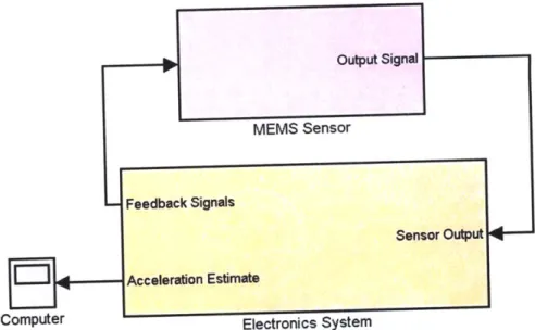
A high level block diagram of the accelerometer system is shown in Figure 2-1. In this figure, the entire electronics system is abstracted into one block. The MEMS sensor receives input signals from the electronics system, and it responds
to these with an output signal. This sensor output signal is then taken into the electronics system where processing and analysis is done. The electronics system produces an acceleration estimate from the sensor output, which it packages and sends to a computer so that readout can be performed. In addition, the electronics system takes this acceleration estimate and uses it to provide the proper input signals into the MEMS sensor.
Output Signal -MEMS Sensor Feedback Signals Sensor Output Acceleration Estimate
Computer Electronics System
Figure 2-1: High Level Block Diagram of Accelerometer System
2.1
Sensor Characteristics
The MEMS accelerometer used for this thesis belongs to a class of MEMS
accelerom-eters known as force-rebalanced acceleromaccelerom-eters [28]. This name refers to the fact
that a force is applied to the MEMS device in order to eliminate unwanted non-linear
effects. To understand how these accelerometers are used in a closed loop system, the
sensor must be understood in more detail. This section describes the workings of the
MEMS accelerometer.
2.1.1
Ideal Sensor Model & Behavior
The sensor around which the preload architecture is designed can be modeled as
an asymmetrical proof mass rotating around a pivot, as shown in Figure 2-2. The
input axis is perpendicular to the plane of the proof mass. Because the proof mass is
asymmetrical, it has more mass on one side of the pivot and applied acceleration on
the input axis causes a rotation around the pivot. This angle of rotation can then be
detected by capacitive pickoff.
Referring to Figure 2-2, the distance between the sense plates and the proof mass
changes as the mass rotates around the pivot. Since the capacitance is inversely
proportional to the distance between the parallel plates, the capacitance thus changes depending on the rotation angle of the proof mass. When a voltage is applied to the sense plate, charge is accumulated on the proof mass according to the capacitor law
Q
= CV. Thus, as the capacitance changes, the amount of charge accumulated on the proof mass changes as well. An external charge amplifier can convert this charge into a voltage level, and thus the rotation of the proof mass can be detected.Movement of the proof mass can be modeled as dynamics of a mass-spring-damper system. The amount of rotation of the proof mass has a non-linear relationship with acceleration, dependent on the spring constant. Detection of the rotation is also non-linear, of the form 1 where g is the distance gap between the sense capacitorsg and the proof mass. This is due to the inverse relationship between capacitance and distance. These non-linearities pose a problem for the electronics system. While the acceleration could be computed using non-linear equations, this method would rely on models of the sensor which may not be fully accurate due to real world non-idealities. In addition, the range of inputs is limited because the proof mass will eventually reach its physical limit of rotation. At this point, the proof mass will not be able to rotate further and stronger accelerations will not be measurable.
A better method for obtaining an accurate acceleration measurement is to ensure
that the proof mass never moves significantly. By running the sensor in a closed loop system, the proof mass can be restored to its null position during operation, thus eliminating the non-linear factors. In the closed loop sytem, the position of the proof mass remains relatively constant and the rebalancing force will have a linear relationship with the input acceleration. This rebalancing force is equal and opposite to the external acceleration torque, and thus the acceleration can be measured.
Four torque plates are used to provide the rebalancing force to the proof mass. Two plates are above and below the proof mass left of the pivot point and the other two plates are on the right side of the pivot point. The left and right torquers provide force around the pivot point in opposite directions. Figure 2-2 shows a side view representation of the MEMS accelerometer, illustrating the torque and sense plates.
Left Upper Torque Left Upper Sense Right Upper Sense Right Upper Torque
I'll
I
Q
Pivot Point
I
T
T
T
T
Left Lower Torque Left Lower Sense Right Lower Sense Right Lower Torque
Figure 2-2: Physical Diagram of MEMS Accelerometer
and the spring and 1 non-linearities can be ignored. In order to design this feedback
9
loop, though, the characteristics of the sensor must still be understood. The sensor characteristics must also be known in order to construct an accurate model of the sensor. Such a model is required in order to design a feedback system that can properly rebalance the sensor.
Although there are non-linear effects regarding the relationship between input torque voltage, input acceleration, and output voltage, the system can be simplified into small signal inputs and the corresponding small signal output. This simplification is possible if we assume that in the final system, the proof mass is restored to the null position. As long as the null position is maintained, simplifications can be made in the ideal model of the sensor. The rotational stiffness and the capacitor non-linear dynamics can both be ignored. In this case, the capacitive pickoff voltage coming out of the charge amplifier is linearly dependent on the input acceleration. This gain term is referred to as the scale factor of the sensor. The scale factor thus has units of
V. In other words, applying a certain amount of acceleration to the sensor will result
9
in a linearly dependent amount of voltage on the output where the gain is given by the scale factor. The scale factor is measured in real world g's where g = 9-8 to
Characteristic Value
Scale Factor
1.5"-Torque Constant 0.29+
Table 2.1: Typical Sensor Characteristics
000--0.01
10 -8 6 4 -2 0 2
Input Acceleration (g) 4 6 a 10
Figure 2-3: Ideal Characterization of Sensor Scale Factor
Again assuming that the input acceleration as well as the input torques are
rela-tively small, the input torque voltages have a square relationship with the position of
the proof mass. The proportionality constant relating rebalanced g's to input voltage
squared is referred to as the torque constant. Rebalanced g's refers to the input
ac-celeration that would be necessary to produce a certain output voltage. The torque
constant could have been given in terms of output voltage divided by input voltage
squared, but the definition in terms of rebalanced g's is more convenient for design
and testing. The torque constant has units of -. Typical values for the scale factor
and torque constant are shown in Table 2.1.
To illustrate the effect of acceleration input on the accelerometer output voltage,
.... ... .... . ...
-- Let Torque AcW Rigto: Torqer Active
023
Torque Plaes DC Volltage M
Figure 2-4: Ideal Characterization of Sensor Torque Constant
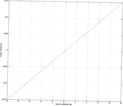
we must assume that the proof mass is at the null position. Of course, this depends
on the system being properly rebalanced, but the initial assumption can be that the
mass does not move. At the null position, the non-linearities mentioned above can be
ignored. If the input torquers are held at OV, the output voltage varies as shown in
Figure 2-3. The x-axis represents the input acceleration in g's, where g
= 9-8m.The
y-axis represents the output voltage. Thus, the slope of this graph is the scale factor
of the accelerometer.
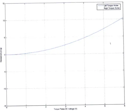
The accelerometer has two sets of torque plates, the left set and the right set.
Applying a certain voltage V to the left set of torquers results in a rotational force
on the proof mass around the pivot. Applying that same voltage V to the right set of
torquers results in an equal and opposite rotational force on the proof mass. Since the
force applied is proportional to the square of the voltage, it doesn't even matter if
+V
or -V is applied, since the force will be proportional to V
2anyways. Assuming there
are no other non-linearities in the system we can create a graph of the acceleration
............ ... ....
Right Torquer Active
Left Torquer Active
% 3
-10 - -ft -2 0 2 4 6 8 10
Input Accelernatin
Figure 2-5: Example Scheme to Rebalance Sensor Using DC Torquing
that would be balanced by a certain voltage applied to each torque plate. This graph
is shown in Figure 2-4.
In Figure 2-4, one curve corresponds to the left torque plate active (with the right
torque voltage at
OV).
The other curve is the opposite situation with the right torque
plate active (with the left torque voltage at OV). This graph implies one rebalancing
methodology for a closed loop accelerometer system. Since we know that both Figures
2-3 and 2-4 hold true when the proof mass is at its null position, we can match the
graphs to each other and figure out what voltage to apply to the torque plates. For
example, if the input acceleration was 10g, 5.9V should be applied to the left torquer.
If the input voltage was -10g, then 5.9V should be applied to the right torquer. This
scheme was used for previous accelerometer designs and works adequately, although
it suffers from a few drawbacks which are mentioned in Section 2.3.2.
Since the relationship between input acceleration and necessary rebalancing
volt-age is known, a scheme can be developed that rebalances the sensor based on the
current acceleration. An example graph of transfer characteristics is shown in Figure
2-5. This is not the scheme used in the preload architecture, but it does help
demon-strate the concept behind force rebalancing the proof mass. In this scheme, when there is a positive acceleration, a DC voltage is placed on the right torquer. When there is a negative acceleration, a DC voltage is placed on the left torquer. Obeying the torque constant scaling factor, the DC voltage shown in Figure 2-5 perfectly re-balances the sensor and keeps the proof mass in the null position. Although this is not the rebalancing scheme used in the preload architecture, this scheme provides a conceptual foundation on which the preload architecture can be built.
2.1.2
Physical Sensor Details & Consequences
As the sensor is being torqued, the torquers cannot simply use a DC voltage to rebalance the proof mass. A DC voltage would build charge on the proof mass, creating another non-linear system as the charged proof mass experiences electrostatic forces with the charged torque plates. In addition, the charge built on the proof mass would affect the charge on the sense plates, thus corrupting the output signal. To counteract this effect, a square wave is applied to the torquer plates so that no net charge builds up on the proof mass. In actuality, charge inevitably does build up on the proof mass, but the torque square wave can operate at a frequency distinct from the sense square wave so that the two do not interfere with each other. An ideal square wave has the same effect as a DC voltage due to the square law. For each pair of torquer plates, the upper plate and the lower plate have opposite polarity input square waves so that at any given moment, they both provide the same direction of force on the proof mass.
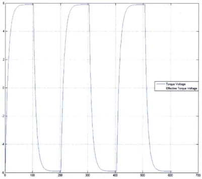
Although an ideal square wave would have the same net torque as a DC voltage, it is impossible for a real electronic system to generate an ideal square wave. Instead, the system generates a square wave with a finite slew rate. An example wave is shown in Figure 2-6. This figure shows the equivalent torquing voltage that could be applied if charge buildup on the proof mass was not a concern. This equivalent voltage is simply the absolute value of the actual voltage placed on the torquer plates. This
Figure 2-6: Finite Slew Rate Effects on Torque Voltage
effective voltage is not a clean DC voltage and is marred whenever the square wave
switches polarity. Thus, the actual torque placed on the sensor is neither constant nor
at the desired voltage level. A non-constant torque is acceptable, as long as we ensure
that the frequency spectrum does not affect the sensor operation or the readout of the
sensor. However, differing slew rates on the left and right torquers (due to mismatched
analog components) will result in differing equivalent DC voltages. The solution is to
purposely reduce the slew rate to a known value so that both left and right torquers
match exactly in their slew characteristics.
2.1.3
Modeling the MEMS Sensor
The MEMS sensor is modeled with the rotational stiffness and capacitive pickoff
non-linearity that occur when the proof mass is rotated. Simulations using the MEMS
sensor model cannot assume that these non-linearities are eliminated; instead, the
simulations must show that the acceleration readout from the electronics is accurate
despite the non-linearities. However, as long as the feedback loop is implemented properly and the bandwidth constraints on the input are properly designed, the po-sition of the proof mass will stay near 0 and the assumptions on the scale factor and torque constant will hold true. Detailed models of various MEMS sensors have been developed by Draper Laboratory engineers and the design of such models is outside the scope of this thesis.
2.2
Electronics Requirements
There are several design requirements that every electronics architecture for the ac-celerometer must obey. For the control loop to close and rebalance the proof mass, the system must be linear time-invariant. The square relationship between the torque input is not a linear relationship; this must be linearized in some way. The preload architecture is able to linearize the system, which will be discussed further in Section
2.3.1.
The sensor output is amplitude modulated to the square wave placed on the sense plates. The electronics must demodulate this signal in order to obtain the proof mass position. The digital electronics must also be capable of reading out the acceleration estimate to an external microprocessor or computer.
While there are no strict requirements on hardware size or power consumption, the minimization of both these characteristics is preferred. An efficient design in terms of hardware and power can be more easily adapted for use in an ASIC. A lower power design will extend the operational lifetime of the electronics system when running on battery power. In addition, the lack of wasteful electronics makes the system simpler and easier to debug.
2.3
Architecture Design
Any architecture that provides feedback for a force rebalanced MEMS accelerometer must be capable of linearizing the feedback loop. In the control loop, the only
non-linear relationship is the square law between the torque voltage and the sensor output voltage. There are a variety of ways to linearize this relationship. The preload architecture has been developed as one way to create a linear feedback loop.
2.3.1
Preload Architecture Concept
With zero input acceleration, the preload architecture uses a bias voltage VB as the amplitude of each torquer square wave. With a non zero input acceleration, a voltage
77a proportional to the readout acceleration is added to one torquer and subtracted
from the other torquer. If the left torquer amplitude is VL and the right torquer amplitude is VR, they can be defined as follows.
VL = VB + V.
(2.1)
VR = VB -V
(2.2)
Thus, the total rebalanced acceleration can be computed as a function of these voltages and the torque constant T.
a TLVZ - TRv = TL(VB 2VBVa V2) - TR(B2 - 2VBVa+V2) (2-3)
If TR and rL are equal, Equation 2.3 can be simplified as follows.
a = 4TVBVa (2.4)
Even if TR and TL are not exactly matched, this can be compensated by sending different VB values to each torquer as well as having different gains on the two Va
signals coming out of the processing. Thus, the control loop has been linearized and a feedback controller can be used to restore the proof mass to its null position. In addition, the Va value that is used to restore the proof mass is proportional to the input acceleration and can be read out to an external processor or computer.
Variable Nominal Value
VB
2.936V
Va
0.2936V
Table 2.2: Nominal Voltages for Preload Architecture
-10 - -6 -4 -2 0 2 Input Accleration (g)
4 6 8 1
Figure 2-7: Preload Scheme to Rebalance Sensor
for the preload architecture. In the preload scheme, both torquers are simultaneously
active so there is more power consumed in the torquers. To minimize this power
consumption, VB should be minimized while satisfying the design constraints listed
in 1.1. Thus, at a
+10g
or a -10g input acceleration, one torquer should be completely
off. Using this realization allows us to solve for nominal values of VB and va. These
values are listed in Table 2.2.
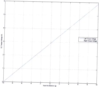
Using the nominal design settings for the preload architecture, we can construct
a graph similar to Figure 2-5 that shows the needed DC torque voltages to rebalance
each possible acceleration in the input range. This graph for the preload architecture
is shown in Figure 2-7. In fact, the nominal voltage for
VBis a minimum value. If
the DC torque voltage were to somehow go negative, this would destroy the linearity
Ld Torquo Vokg. Right Torque Voket.
of the preload architecture. The square law of the sensor guarantees that only the absolute value of the torque voltage matters. In addition, the torque plates actually receive a square wave modulated voltage instead of a DC voltage. So the supposed negative DC voltage torque would actually end up being an unintended positive value. Figure 2-7 shows the input and output characteristics for a perfectly rebalanced sensor. The major difference between this graph and Figure 2-5 is that in the preload scheme, the torque magnitudes are always a linear function of acceleration. By con-trast, the scheme where only one torquer is active has a square root relationship with the input acceleration.
2.3.2
Alternative Architecture
An alternative design to the preload architecture is an electronics system designed to rebalance the sensor using the scheme shown in Figure 2-5. In this scheme, either the right or left torquer is activated depending on whether the input acceleration is positive or negative. The inactive torquer receives a OV signal.
A control loop can be designed to rebalance the sensor so that the proof mass
remains in the null position. Since there is an inherent square law in the sensor, the control loop must contain a square root function in order to linearize the feedback path. In addition, there must be a sign selector bit that determines whether the left or right torquer is active.
The requirements of the alternative architecture's control loop present several dis-advantages. Performing a digital square root computation is relatively wasteful and impractical compared to the strictly linear operations needed for the preload architec-ture's control loop. An algorithm such as Dijkstra's square root algorithm in digital logic requires multiple clock cycles to converge to a solution and requires a relatively large area of hardware [27]. Multiple clock cycles of processing time is disadvanta-geous since this increases the latency of the control loop. A control loop with more latency has a higher time constant and is slower to respond to perturbations, thus leading to decreased accuracy in the system. The feedback system relies on move-ments in the proof mass quickly being compensated; a slow feedback time constant
means that the non-linearities cannot be ignored since the proof mass will be slow to move back to the null position. A large area of logic is also a problem. The system will eventually be migrated to an ASIC and extra space results in added cost and added power consumption.
As mentioned above, a sign selector bit is necessary in the alternative architecture to indicate which torque plates are active. This sign bit causes problems, especially around 0g. Around Og, it is critical that the sign selector bit is perfectly synchronized with the torque magnitude; otherwise, the system will be attempting to rebalance in the wrong direction. While the feedback loop will ensure that the system remains stable, this will still lead to inaccurate measurements around 0g since it is impossible to perfectly synchronize these signals independent of temperature. In addition, at exactly Og, the sign bit will show up as a white noise source since external noise will cause the indicated acceleration to flicker between positive and negative values. This white noise sign bit causes capacitive coupling problems with other signals, further reducing the system's accuracy at 0g.
The preload architecture is able to eliminate the problems of both the digital square root and the sign selector bit. While it suffers from its own drawbacks (notably, higher torque power consumption), it does not suffer from accuracy problems around
0g. It is capable of a lower latency, since it does not have any iterative algorithms in
the control loop. Finally, the preload architecture should be able to have a smaller physical size due to a reduced amount of logic.
2.4
Analog & Digital Subsystems
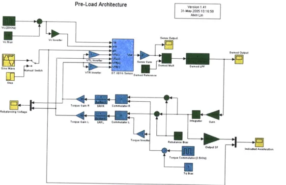
Figure 2-8 shows a representation of the electronics design needed for the preload architecture. Coming out of the sensor, the sense gain and anti-aliasing filter are built into the accelerometer interfacing ASIC, so they are outside the scope of this thesis. Every other component shown in this diagram (with the exception of the sensor) is designed and implemented.
Version 1.842 01-Aug-2005 10 3529
Pre-Load Architecture
A
n unsu e
sip
aV
ilei
Spea
Anf
Sgh.Di gi
Dsad
ToWVT invde DT)010 Sanse r SD "
Sma
t
Rate
aloq soLPFiR
TorqRegulNto
-
bTtiga
n
SM R R SAt R4
ign
by
sna ro
Ced
modlatd sgna ino abasbad vlue A th rde COdeim
tio
SFilerniaeduAesto
theamplratgasrel as8 Preomadwps Arhiecur notchtrns Overichwilbfute
ofnterge an contlliaknfle an pematio furheor hedit spine th controltao
hasoeelatoretrized the raoutiga coul atually hia beena taket from seea paces
inthy o here l
higa signalesig propotonal dt
al.eouaoun
h
mltd
moatedh otor h signalaloge into a
2ndad au. t order CIC intoation filterus
thtiessthe sample rate.aspefom
nextas bloc cnsitch fltnhh oprains to puer
the preoidn arhecturk opeation keescriedroo Eqaihlpstions .n..
ATehe tput
torquee vltagesaree cuaedutheudculy goithweare sigmdeta frodevraulatosesa
oversample the digital signal to push the quantization noise out of band.
After the torque signal sigma-delta modulators, analog circuitry is needed to create
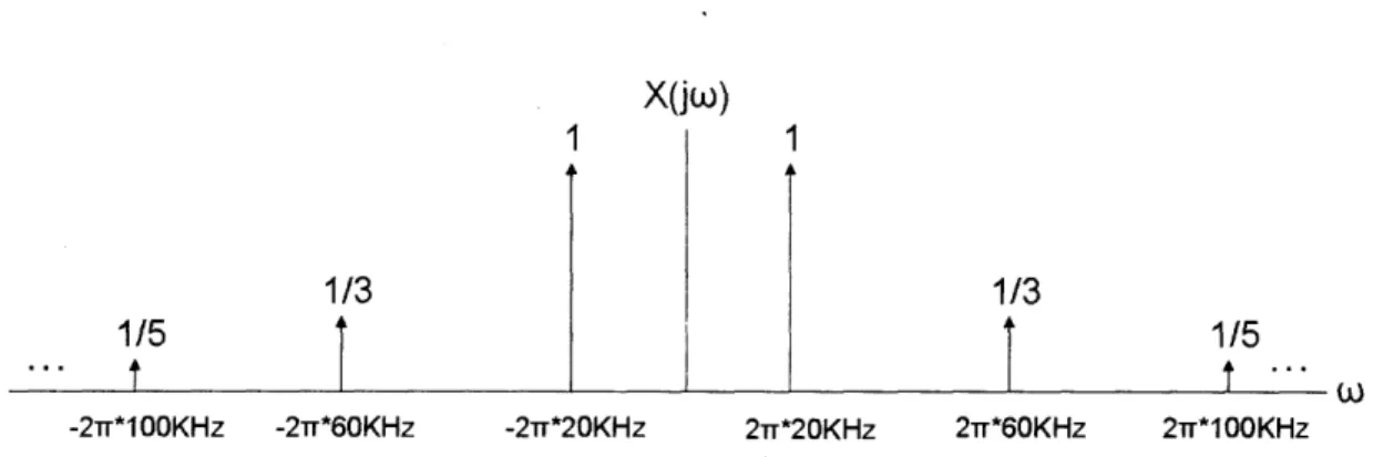
X(joW)
1/5
1/3
1
-2Tr*100KHz -2-r*60KHz -21T*20KHz1/3
1/5
2r*20KHz 2-r*60KHz 2rr*100KHzFigure 2-9: Frequency Spectrum of Ideal 20KHz Square Wave
the proper torque voltages. An analog low pass filter eliminates the modulation of the
sigma-delta modulator and creates a baseband signal. Next, a regulator adjusts the
digital voltage level to the proper analog levels. The signals must then be amplitude
modulated to the torque commutation frequency to avoid charge buildup on the
sensor. The slew rate of the commutated torque signals must be limited with another
low pass filter to match slew rates on all torque signals. A final inversion is necessary
on some torque signals before they enter the sensor.
2.5
Frequency and Sample Rate Selection
Signal
Nominal Value
Sense Generator
20KHz
Digital Input Sample Rate
5.12MHz
Digital Processing Rate
20KHz
Output Sample Rate
625Hz
Digital Output Sample Rate
5.12MHz
Torque Commutator
2.5KHz
Table 2.3: Nominal Frequencies and Sample Rates for Preload Architecture
There are various analog and digital signals in the preload architecture that require
frequency and/or sample rate selection. They must be carefully picked to avoid
interfering with each other while insuring proper operation of the sensor. Nominal
values for these frequencies and sample rates are shown in Table 2.3.
A sense generator frequency of 20KHz is used for this specific accelerometer due
to the physical characteristics of the sensor. With this sense generator frequency, the proof mass position is amplitude modulated to 20KHz. Assuming the only spectral content of the sensor output is at 20KHz, then a digital input sample rate of 40KHz would be necessary to sample the signal. However, the sense generator is a square wave and thus the input signal has many harmonics that will cause aliasing in the spectrum of interest if the input sample rate is set too low. The anti-aliasing filter built into the accelerometer interface ASIC has its cutoff frequency at 2MHz, so it cannot be counted on to eliminate these harmonics.
The spectrum of an ideal 20KHz square wave is depicted in Figure 2-9. Harmonics are present on all odd multiples of the carrier frequencies. The magnitude of the harmonic goes down inversely with the multiple. For example, the magnitude of the harmonic at the 7th multiple of the carrier frequency is I the magnitude of the carrier frequency. Thus, if we choose 5.12MHz to be the sample rate, the harmonic at the Nyquist frequency of 2.56MHz has a magnitude of 2 042H, = 7.81 * 10-3 assuming
the carrier has a magnitude of 1. This represents at least 42.14dB of attenuation
(referenced to the carrier) on the harmonics that will be folded down into the spectrum of interest. However, the output signal of the sensor is not an ideal square wave so the attenuation at higher frequencies is even higher than this. In addition, the interface
ASIC contains an anti-aliasing filter with a cutoff at 2MHz, so the aliasing is negligible.
The bulk of the digital processing occurs at a lower sample rate than the input sample rate to the digital subsystem. Once the signal comes in, digital signal pro-cessing can be performed to avoid aliasing and corruption effects from analog noise, capacitive coupling, and the expected harmonics from the square wave. The signal does not need to be processed at 5.12MHz, especially with an input bandwidth limit of 100Hz. Although it could be processed at this speed, such processing would be very wasteful on power, since many more operations than necessary would be performed. Instead, the main signal processing is performed at 20KHz. This frequency is much more than necessary to fully represent the 100Hz range of data. However, the signal processing should not be set too low; otherwise, the latency of the loop would increase
and have negative effects on the feedback response. In addition, the ratio of 5.12MHz
to 20KHz has convenient aspects in regard to the CIC decimation filter, which will
be further explained in Section 3.3.
The output sample rate refers to the signal that is transmitted to a computer.
625Hz was chosen for this sample rate because it is capable of fully representing the
100Hz input bandwidth. This signal is not in the feedback path, so latency is not
a concern with this relatively slow sample rate. 625Hz also divides into 20KHz by
a power of 2, allowing efficient decimation. Finally, 625Hz is sufficiently slow that
64-bit data could be transmitted into a PC's serial port at that rate.
The output was interpolated back up to 5.12MHz in preparation of entering the
D/A sigma-delta modulator. 5.12MHz was chosen as a sufficiently high oversampling
ratio for the sigma-delta modulators, pushing the noise out of band.
The torque commutator frequency had to be chosen to not interfere with the
sense generator frequency. Due to the proximity of the sense generator plates and
torque plates in the MEMS accelerometer, there is substantial coupling between the
torque plates and the charge pickoff on the sense plates. Thus, a 2.5KHz square
wave is used for the torque commutation frequency. This square wave only has odd
harmonics, so it does not contain a harmonic at 20KHz. The harmonics that appear
at 17.5KHz and 22.5KHz are a concern, but can be filtered out if they pose a problem.
In addition, 2.5KHz for the torque commutators is fast enough to avoid the charge
buildup problem where charge accumulates on the proof mass.
2.6
Functional Simulation
The preload architecture was simulated at varying levels of complexity. Before
de-tailed models of the digital components were constructed, a system level simulation
was first constructed. In this system level simulation, the details regarding the inner
workings were abstracted into functional blocks. A Simulink model for this functional
simulation is shown in Figure 2-10. The purpose of this simulation model is to verify
that the preload architecture can properly rebalance the accelerometer and properly
Pre-Load Architecture version 1.41 31-May2005 10 16 50-AMn Un sensei outputd Ve ElioaE DrmidOtput VTLof the senaion
aInDd o
Mtprove
LPa t
ev er is. pVTRrnr
et DT im
S Dde
eee CStep
Torque
T iin
R SRFR
Commutato
R
c
Reolation Voltage
O
Torque
ogin
L SRFL
Commtim
siul ati
oTo,. rvi t Rebalanc Bins
Torque Com. ae gC.61012)
Tqitas
Figure 2-10: Functional Model Setup for Preload Architecture
read out the input acceleration.
In this model, many of the implementation details have been eliminated in an
attempt to create a working closed loop simulation to prove that the preload
archi-tecture works in concept. There is no discrete time processing in this model. Instead,
everything is processed in continuous time. The CIC decimation filter has been
re-placed with a continuous time low pass filter, since there are no sample rates to
convert. The digital PI controller is replaced with a gain and an integrator. The
interpolation filter and sigma-delta modulators are completely eliminated since they
have no meaning in a continuous time simulation.
The simulation results from this functional model are shown in Figure 2-11. The
input waveform is a 10g amplitude sine wave at 100Hz. The output readout has
some noticable latency and attenuation; both of these factors are expected due to the
transfer characteristics of the control loop.
Time (sec)
Figure 2-11: Functional Model Simulation Results
Chapter 3
Digital Design
The majority of the signal processing for the preload architecture is performed in the digital domain. Generally, performing computations in the digital domain is beneficial when there is a large amount of data that needs to be processed quickly and accurately [2]. Digital circuitry is ideal for this application because it is resistant to electrical noise and temperature effects as well as being robust to process variations during manufacturing [9].
This chapter first provides an overview of the digital system and explains the required function of each component block. Next, it goes into detail on the design and
implementation of each block. Finally, a synthesis analysis is presented, comparing the implementation size of the various components.
3.1
Digital Overview
An overview of the digital subsystem is shown in Figure 3-1. In this diagram, the analog blocks have been compressed into abstract subsystems while the digital blocks are shown in relative detail. The signal coming in from the analog input stage is a sigma-delta modulated signal at 5.12MHz. This is a 1-bit signal with a sample rate of 5.12MHz, and it represents the sensor signal amplitude amplitude modulated at 20KHz. Thus, the signal needs to be demodulated to move the signal to baseband.
Tq W.ar
Figure 3-1: Digital Subsystem Block Diagram
filter is used to reduce the sample rate. Separate from the feedback
path, another CIC
decimation filter is used to further decrease the sample rate to 625Hz
so that it can be
transmitted to a computer. Before being transmitted, this data
is packaged using a
UART transmitter so that it can be received by the software running
on the computer.
In the feedback path after the digital compensator, the signal is interpolated
back up
to 5.12MHz. Several math operations are performed on the signal
in order to compute
the proper rebalancing voltages for the torque plates. These math
operations comprise
the core operation of the preload architecture and are represented
in Equations 2.1
and 2.2. Finally, the signal goes through a D/A sigma-delta
modulator to transmit
the torque amplitudes back into the analog domain.
All signals in the DSP path are represented as two's complement
fixed point
values between -1 and +1. Thus, the most significant bit (MSB) is
the sign bit and
all other bits represent the fractional value of the signal. Fixed point
representations
in the feedback loop have the advantage that they result in smaller
and simpler
hardware than the analogous floating point logic
[4].
Using two's complement fixed
point representations, the precision of each register can easily be controlled
by simply
adding more least significant bits to the register.
3.2
Demodulator
The first digital stage in the preload architecture is the demodulator. The demodula-tor is necessary because the output of the sensor is amplitude modulated to the sense generator signal, which is nominally 20KHz. The demodulation can be performed by multiplying the incoming signal by a 20KHz sine wave perfectly in phase with the sense generator square wave. In actuality, the signal coming in from the sigma-delta modulator is slightly out of phase with the demodulation reference due to analog de-lays. This discrepancy manifests itself as a constant phase delay and thus a constant gain error (with absolute value less than 1) on the demodulated output. The phase difference was experimentally measured to be small, so the gain error was negligible.
There are several ways to generate the digital sine values necessary for the de-modulation. One of the simplest and most effective methods is by table lookup [16]. In this method, the values of the sine are precomputed and stored in a ROM and referenced by an index. The drawbacks to this method is that the precomputed values must be rounded and are only available for quantized time instances. In the preload architecture, this is not a problem because the sample rate is fixed and the precision of the sine values can be arbitrarily increased as necessary by increasing the bits for each sample.
As an optimization of ROM size at the expense of more logic, only the first quadrant of the sine wave is stored in the ROM. Using this information, the value of the entire sine wave can be determined at any phase value. Another optimization is that the sign bit of the sine wave is not stored in the ROM. Since only the first quadrant of the sine wave is stored, the sign bit is known to be always 0, indicating a non-negative number. Simple logic can be used to determine the proper sign bit and values in the other quadrants of the sine wave. The demodulator functions as a digital multiplexer. When the sigma-delta modulated input is high, the output is the current value of the demodulator reference. When the sigma-delta modulated input is low, the output is the inverted value of the demodulator reference.