HAL Id: tel-02908238
https://tel.archives-ouvertes.fr/tel-02908238
Submitted on 28 Jul 2020HAL is a multi-disciplinary open access archive for the deposit and dissemination of sci-entific research documents, whether they are pub-lished or not. The documents may come from teaching and research institutions in France or abroad, or from public or private research centers.
L’archive ouverte pluridisciplinaire HAL, est destinée au dépôt et à la diffusion de documents scientifiques de niveau recherche, publiés ou non, émanant des établissements d’enseignement et de recherche français ou étrangers, des laboratoires publics ou privés.
To cite this version:
Akanksha Kapoor. Core-shell InGaN/GaN wire for Flexible LEDs. Materials Science [cond-mat.mtrl-sci]. Université Grenoble Alpes, 2020. English. �tel-02908238�
THÈSE
Pour obtenir le grade de
DOCTEUR DE L’UNIVERSITE GRENOBLE ALPES
Spécialité : NANOPHYSIQUE
Arrêté ministériel : 25 mai 2016 Présentée par
Akanksha KAPOOR
Thèse dirigée par Joël EYMERY et codirigée par Christophe DURAND
préparée au sein du Labor atoire PHotonique, ELectronique et Ingéniérie Quantiques (PHELIQS)
dans l'École Doctorale Physique
Core-shell InGaN/GaN wires for Flexible
LEDs
Thèse soutenue publiquement le 4 June 2020 devant le jury composé de
Prof. Peter James Parbrook University of Cork, Ireland, Rapporteur Prof. Jean-Paul Salvestrini
Georgia-Tech Lorrain, Rapporteur Prof. Agnès Trassoudaine
Université Clermont Auvergne, Examinatrice Dr. Thierry Baron
Directeur de recherché, CEA-LTM, Président du Jury Dr. Maria Tchernycheva
Directrice de recherché, C2N Paris, Examinatrice Dr. Benjamin Damilano
Chargé de recherché, CNRS-CRHEA, Examinateur Dr. Joël EYMERY
Directeur de recherché, CEA/IRIG/MEM, Directeur de thèse Dr. Christophe DURAND
With all due respect dedicated to my parents -
Archana & Vimal
ACKNOWLEDGEMENT
The journey of my Ph.D. not just helped me to learn plenty of scientific skills but also instilled me with personal developments. The questions like ‘Why’ and ‘How’ have now increased in my mind. I feel fortunate to be welcomed at CEA Grenoble, an organization filled with scientific experts in abundance. Looking back at every single day of my thesis, I now believe that great accomplishments are a result of patience, hard work and dedication.
This work could be possible only with the huge support of my supervisors who kept pushing me to give my best. First and foremost, I would like to express my sincere gratitude to my thesis supervisor Dr. Joël Eymery. I was always inspired by his vast knowledge and never ending enthusiasm towards the subject. His supervision taught me that ‘no result is also a result’ in a scientific domain. He guided me with significant remarks and showed me the right direction when I had several choices ahead of me during the experiments. This greatly enhanced the quality of my work.
I extend my heartfelt acknowledgement to my thesis co-supervisor Dr. Christophe Durand. His guidance gave me pedagogical insights and helped me to thoroughly understand the results. The hours of productive discussions with him increased my curiosity towards the subject, making me enjoy my own work. He always motivated me and had faith in me. His positive approach also helped me to overcome the difficulties faced during experiments.
I would like to thank Henri Mariette (former director of NPSC), Régis André and Bruno Gayral (directors of NPSC), and Jean-Michel Gerard (director of PHELIQS) for making the laboratory a warm and friendly place. I also acknowledge the French laboratory of excellence - GANEX for funding my thesis project. I sincerely thank Jean Dussaud for his technical expertise regarding the MOCVD system. Many issues have been faced in the equipment one after the other and could only be managed with his constant help and support.
guidance of Dr. Maria Tchernycheva (at C2N, Paris) during my Ph.D. work. She welcomed me at C2N to provide me with trainings regarding device fabrication and their detailed electrical characterizations. I would like to thank Dr. Catherine Bougerol for providing us with important TEM measurements followed by detailed discussions. Her constructive feedback helped me to comprehend the results in a better way. In addition, she also helped me in my defense rehearsal and I have always found a mentor in her who encouraged me during all these years. I would like to acknowledge Dr. Eric Robin (at CEA/IRIG/MEM, LEMMA Laboratory) for his help in EDX measurements. His support helped me to obtain some new and interesting results during the final year of my thesis. My sincere thanks goes to Dr. Gwenole Jacopin (at Institute Néel, CNRS) for his enormous help in the cathodoluminescence measurements which form an important part of my thesis work. He helped me in analyzing the results and delivering some new perspectives through regular discussions, giving me a clear understanding of my work. I could perform other optical characterization in my work, thanks to the support of Dr. Bruno Gayral, Dr. Eva Monroy and Dr. Joel Bleuse. They helped me in the installation of the setups and have been always available to resolve the experimental issues or my scientific queries.
I would like to thank Dr. Jean Paul-Barnes (at CEA-Leti) for his support and guidance in ToF-SIMS measurements. His clear explanations and productive comments allowed me to learn the technique efficiently. I sincerely acknowledge the support of Dr. Gilles Le Blevennec (at CEA Leti’s Optics and Photonics Division (DOPT)). He not only provided me with different phosphors but also helped me in performing their detailed characterizations.
A major part of my thesis work involved activities that were performed at PTA clean rooms. I am very thankful to Marlène Terrier, Thierry Chevolleau, Thomas Charvolin, Jean-Luc Thomassin and Frédéric Gustavo for their cooperation and advices during fabrication process of the devices.
I deeply appreciate the assistance of other fellow colleagues in my team namely, Martin Vallo for presenting me the clean room activities and wire growth, Amine EL Kacimi for introducing me to
FIB preparation of the wires.
I consider myself fortunate to be welcomed by a lively and cheerful NPSC team. I got the opportunity to meet many other young scientists in the team and our journey of thesis together brought some of us in a strong bond of friendship: Madalina, Marion, Maria, Vincent, Saptarshi, Akhil, Alberto, Houssaine, Nathaniel, Saransh, Guillerme, Anjali, Romain, Ioanna, Alexandre, Tan, Farsane, Remy, Jane & Sergi. I received some good French learning exercises during my lunch time with Catherine, Yann and Houssaine. I would also like to give a special mention to Monika and Nitika, my Indian friends who were not less than a family in Grenoble. I will always cherish our endless talks during dinner.
I also owe gratitude to my mentor back in India – Prof. S. Annapoorni who laid a strong foundation of Physics in my career and helped me to work hard for a bright future.
Lastly, I would like to thank my mom, Archana and my dad, Vimal from the bottom of my heart for their constant love and blessings. Thank you for inspiring me and teaching me to work with dedication and honesty. Special thanks and love to my brother, Utkarsh for making me laugh during the grim of times. I am also grateful to Lakshay who stood as a pillar for me during these years.
ॐ॥ जय गुरूजी ॥ॐ
OUTLINE
Introduction………..1
1. Background of Nitride based visible LEDs studies 1.1 Basics of nitride semiconductors….………...…….6
1.1.1 Crystal structure………..6
1.1.2 Polarity………7
1.1.3 Lattice mismatch……….8
1.1.4 Polarization………...9
1.1.5 Band gap………...11
1.2 Conventional nitride based LEDs using planar structures.………12
1.2.1 Standard structure on sapphire………...…………...12
1.2.2 Ways to improve light efficiency……….………….13
1.2.3 Demonstration of green LEDs………..……….16
1.3 Moving towards wire-based LED………...…………..19
1.3.1 Benefits of wires over planar based LEDs……….19
1.3.2 Different ways to grow GaN wires………...21
1.3.3 Demonstration of MOVPE grown wire-based LEDs…………..………..……23
1.3.3.1 Early demonstration of blue emission……….…..23
1.3.3.2 Achieving white LEDs using phosphors………...………27
1.4 LEDs with additional functionality of flexibility………..….29
1.5 Objectives of the present thesis………..………..…….32
References………..………...……33
2. Growth of InGaN/GaN core-shell wires by MOVPE 2.1 Self-assembled (SG) and self-catalyzed growth of wires………..44
2.1.1 Basics of MOVPE growth technique………...44
2.1.2 Catalyst-free growth of GaN wire with silane addition……….46
2.2.2 Inhomogeneities in indium composition……….………..………52
2.2.3 Length variations in wire-assembly………...………..……….…54
2.3 Route to achieve uniformity in wire lengths: Organized wires……….…57
2.3.1 Methodology involved in selective area-growth (SAG) on sapphire…………57
2.3.2 Difficulties related to SAG and reproducibility control……….59
2.3.2.1 Influence of silane flow………...60
2.3.2.2 Technological issues in fabricating the SiNx mask………...61
References………..…...64
3. Control of wavelength emission from m-plane InGaN/GaN radial QWs 3.1 State of the Art………..68
3.1.1 Blue emission: Previous work by the group………..68
3.2 Green emission………..72
3.2.1 Growth of InGaN QWs as a function of QW growth temperature………72
3.2.2 Optical characterization using photoluminescence (PL) and cathodoluminescence (CL)……….………..74
3.2.3 Structural characterization using STEM combined with EDX...………...76
3.2.4 Estimation of indium content in QWs by atomic probe tomography (APT)….78 3.2.5 Electroluminescence (EL) of single wire device………...………79
3.2.6 Challenges to achieve reproducibility in green emission………..…81
3.3 Dual color emission………...87
3.3.1 MOCVD growth and structural observation……….…..……...87
3.3.2 Optical Characterization………...88
3.3.2.1 Temperature dependent PL (TDPL) and power dependent PL (PDPL).88 3.3.2.2 Low temperature CL measurement…………..……….90
3.3.3 Structural Characterization………...91
3.3.3.1 STEM observation………92
3.3.3.2 In-content profile by EDX analyses………..94
4.1 State of the Art………..………..104
4.2 Investigating the role of GaN-spacer and InGaN underlayer on m-plane InGaN SQW………...105
4.2.1 MOCVD Growth and structural observation…….……….….…105
4.2.2 Optical characterization using PL and CL.………...………..107
4.2.3 Estimating carrier lifetime using time resolved (TRCL) measurements……..110
4.3 Understanding the influence of GaN spacer growth on InGaN QW by STEM and EDX analyses………...………...………..112
References………...117
5. Integrating wires in flexible LED device 5.1 Fabrication of flexible LED devices………..………...………..124
5.1.1 Ni/Au deposition for ohmic contact……….………..…….……...124
5.1.2 Wire encapsulation in PDMS matrix…….……….………..………..125
5.1.3 Ti/Al/Ti/Au deposition for n-GaN contact…..………...……..…..…130
5.1.4 Dispersing silver nanowires for p-GaN contact..………...………….…130
5.2 EL from LED device based on wire-assembly……….………..132
5.2.1 Demonstration of blue, green, dual-color and multi-color emission………..133
5.2.2 Discussion about current injection………..………139
5.2.3 Origin of wavelength variation in wire-based LED………….………..142
5.3 The color control in LED using phosphor down conversion………..146
5.3.1 Investigating yellow phosphors dispersed in PDMS………..146
5.3.2 Study of the fluorescence from phosphors excited by a blue LED…………149
References……….………..152
1
INTRODUCTION
Escalation of GaN LEDs
The first epitaxial growth of GaN by hydride vapor-phase epitaxy (HVPE) technique in 1969 at Radio Corporation of America (RCA) was indeed the beginning of a new revolution in the LED industry. Even if a high threading dislocation density and difficulties with p-type doping came across, the material seemed promising to researchers for making blue LEDs. Eventually, a Mg-doped GaN LED was reported in 1972 but showed a poor efficiency due to high contamination present in the HVPE process.* This slowed down the further research to realize GaN blue LEDs until Amano and Akasaki
reported a significant improvement in the optical and electrical properties of GaN film in 1986.†
The films were grown by metal organic vapor phase epitaxy (MOVPE) with use of low temperature AlN buffer layer on sapphire substrates. They also proposed a method to p-dope GaN by the activation of Mg atoms with the help of electron beam excitation.‡ With this new demonstration
(n-doping was much easier), the first GaN LED functioning as a p-n junction was reported. Unfortunately, this was practically cumbersome for the industrial production and it was still not possible to tune the emission color. The work was then fueled by the remarkable efforts of Nakamura and Mukai in 1991 who produced highly p-type Mg-doped GaN films using thermal annealing.§
They also developed high quality InGaN layers and revealed that the luminescing can be varied in the blue-violet range by changing the indium content in the InGaN alloy.** Finally the first
InGaN/GaN based blue and green LEDs and laser diodes were established and soon
* Maruska, H. P. et al. Violet Luminescence of Mg-Doped GaN. Appl. Phys. Lett. 1973, 22 (6), 303–305.
† Amano, H. et al. Metalorganic Vapor Phase Epitaxial Growth of a High Quality GaN Film Using an AlN Buffer Layer.
Appl. Phys. Lett. 1986, 48, 353–355.
‡ Amano, H. et al. P-Type Conduction in Mg-Doped GaN Treated with Low-Energy Electron Beam Irradiation (LEEBI).
Jpn. J. Appl. Phys. 1989, 28 (12), L2112–L2114.
§ Nakamura, S. et al. Thermal Annealing Effects on P-Type Mg-Doped GaN Films. Jpn. J. Appl. Phys. 1992, 31 (2), 139– 142.
2
commercialized.††,‡‡ This also opened a range of other applications such as solar cells and
photodiodes. The novel discoveries by Amano, Akasaki and Nakamura thus awarded them with a Nobel Prize in 2014.
The GaN blue LEDs have largely replaced the conventional light sources like incandescent bulbs and fluorescent lamps and are widely commercialized especially when combined with phosphors to emit white light. A huge development over the past few years have also led to the achievement of green and even red emission from GaN based LEDs but with a low efficiency. The standard LED design consists of a planar InGaN/GaN thin film heterostructure that has exhibited a high external quantum efficiency (EQE) of 84.3% for blue emission.§§ Further improvement in the efficiency can
be obtained from these structures if we are able to address optimization issues like light extraction, efficiency droop and in-built electric fields. The use of nanostructures such as nanowires (NWs) have the potential to overcome some of the issues faced in thin film LED. Thanks to their smaller footprint and high surface to volume ratio, NW based LEDs can be obtained with a larger lattice mismatch, lower defect density and higher light extraction. The growth of active InGaN QWs on the non-polar sidewalls in NW geometry suppresses the built-in electric fields increasing in theory the radiative efficiency of the device.
Peculiarities from the Laboratory
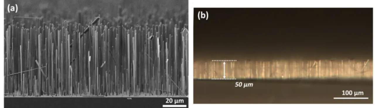
The extensive work performed in our laboratory over the past few years has focused on the MOVPE growth of GaN wires covered by core-shell InGaN/GaN quantum wells. The approach to grow GaN wires with silane addition has been developed in our group in 2010 and facilitated the growth of ultra-long wires on full 2-inch sapphire substrates. Soon, the growth of m-plane InGaN QWs around the wire sidewalls allowed achieving a blue InGaN/GaN wire LED emitting at 410 nm.
†† Zhang, M. et al. Candela-Class High-Brightness InGaN/ AlGaN Double-Heterostructure Blue-Light- Emitting Diodes.
Appl. Phys. Lett. 1994, 64 (13), 1687.
‡‡ Nakamura, S. et al. InGaN-Based Multi-Quantum-Well-Structure Laser Diodes. Jpn. J. Appl. Phys. 1996, 35 (2), L74– L76.
§§ Narukawa, Y. et al. White Light Emitting Diodes with Super-High Luminous Efficacy. J. Phys. D. Appl. Phys. 2010, 43,
3
Simultaneously, the unique method to fabricate flexible LEDs with core-shell wires was established in collaboration with the C2N laboratory by mechanical lift-off of embedded-wire in a polymer. The first flexible blue LED was achieved in the group in 2015. A flexible white LED was also demonstrated very soon by combining the blue LED with phosphors. These achievements are a result of strong collaboration among teams working at INAC/CEA, Grenoble and C2N, Université Paris-Sud. The growth and optical studies of the wires were carried at CEA Grenoble under the supervision of Jöel Eymery and Christophe Durand. The group of Maria Tchernycheva at C2N, Paris focused their activity on the flexible device fabrication and their electrical characterization.
After these breakthroughs achieving different interesting results by the team so far, the goal of the present thesis is to gain a reproducibility control and perform further optimizations of the previous results. The work also targets to achieve longer wavelength emission than blue from core-shell geometry, which has been challenging so far due to difficulties related to In-rich QWs. A color mixing in the single core-shell wire aiming dual-color wavelength emission is also targeted. The previous work concerning the white light emission using phosphors needs further improvement. The optimization of phosphors to be combined with the blue LED in terms of phosphor particle size and composition can allow to gain higher efficiencies. In order to achieve these objectives, the overview of the Ph.D. thesis will be the following:
Organization of the Manuscript
Chapter 1 will give a background of the nitride LEDs studies and realizations. The basic properties of the nitride semiconductor will be briefly summarized. The different design structure of planar LED shall be presented followed by a discussion about the typical issues of light extraction and efficiency droop reported for these LEDs. An alternative approach of using NW LEDs would be proposed explaining their various benefits compared to thin films. An approach of demonstrating flexible LEDs will also be provided, highlighting some novel achievements of the group. The chapter will finish by explaining concisely the objectives of the thesis.
4
The details about m-plane InGaN/GaN core-shell wire growth will be focused in Chapter 2. The growth of GaN wires with silane addition will be explained followed by the influence of different growth parameters to obtain m-plane radial InGaN QWs. Various heterogeneities encountered during the wire growth such as mixing of wire polarity, inhomogeneities in indium incorporation, and non-uniformity in wire length will be explained. The selective area growth (SAG) shall also be presented containing the technicalities involved in mask fabrication and to check the reproducibility control.
Chapter 3 illustrates different wavelength emission from m-plane InGaN/GaN core-shell heterostructures by tuning the indium content inside InGaN QWs. A reproducibility control will be first tested for the blue emission. A detailed study combining structural, optical as well as electrical properties will be then performed to target green emission from m-plane radial QWs in core shell geometry. A dual color wavelength emission from core-shell wires is also targeted with two different families of InGaN QWs containing different indium content.
Chapter 4 is dedicated to the improvement of efficiency for blue emission. The influence of an InGaN under layer (UL) and GaN spacer will be investigated in core-shell wires containing single InGaN QW with a detailed study using different optical measurements like photoluminescence (PL), time-resolved cathodoluminescence (CL) as well as structural characterization including STEM and EDX analyses.
Lastly, Chapter 5 will detail the technology involved in flexible device fabrication and the electrical measurements of the fabricated devices. The different steps involved in the fabrication process carried out in clean room environment will be thoroughly explained. Different flexible devices with blue, green, multi-color and dual color wires will be focused to be measured with electroluminescence (EL). The device fabrication will also be followed by some preliminary work performed with phosphors. Optimization of phosphors slabs in terms of composition and thickness will be focused to be combined with the blue LED to improve the white light emission.
Chapter 1: Background of Nitride
based visible LEDs studies
This chapter provides an overview about the studies and realizations of GaN-based LEDs. The basic properties of the nitride semiconductors are described in the first section including the crystal structure, crystal polarity, lattice mismatch with different substrates and the electronics structures. The second section presents basic designs for planar LED structures followed by the commonly reported issues like poor light extraction and efficiency droop. Different heterostructures such as the use of surface texturing to efficiently extract the light, incorporating electron blocking layer (EBL) to prevent electron leakage, integrating superlattices beneath the active QW region are discussed. The benefits of utilizing nanowires for LEDs compared to thin film LEDs are presented in the third section followed by different ways for growing GaN wires by bottom-up approach using metal organic chemical vapor deposition (MOCVD). Different NW LEDs achieved by various groups are discussed. Some details stressing on an additional functionality of flexibility in LEDs have been provided in the fourth section highlighting the previous achievements of the group. Finally, the chapter finishes by highlighting the objectives of the present thesis work.
6
1.1 Basics of nitride semiconductors
This section will present the brief summary of basic properties of III-N semiconductors. It includes their crystal structure, polarity, lattice mismatch, polarization fields and band gap.
1.1.1 Crystal structure
There are three possible crystal structures for group-III nitride semiconductors (GaN, InN, AlN) namely, wurtzite (α-phase), zinc-blende (β-phase) and rocksalt (γ-phase). The γ-phase can appear only at high pressure and is not stable. The other two phases can be epitaxially grown though the wurtzite structure is thermodynamically stable. It has two hexagonal compact sublattices shifted by 3 8⁄ [0001] with respect to each other, as shown in Figure 1.1 (a), where the length of the hexagon and the edge length is represented by ‘c’ and ‘a’ respectively. The internal displacement parameter ‘u’ is defined as the anion-cation bond length that is also the nearest-neighbour distance in the crystal divided by the lattice parameter ‘c’. The c/a and u/c ratios for an ideal wurtzite structure are 1.633 and 0.375 respectively, however a certain deviation occurs for the real structure. The lattice parameters of wurtzite III-nitrides at 300 K is listed in Table 1.11 while the lattice parameters for a ternary alloy like AxB(1-x)N are approximated by Vegard’s law:
aAB = x aA + (1-x) aB ; cAB = x cA + (1-x) cB ……(Eq. 1.1)
The Miller-Bravais indices denoted by h, k, i and l are used to identify the crystal planes in a hexagonal unit cell with the sum of first three indices necessarily zero: i = - (h + k). The (0001) plane in a wurtzite crystal is along polar direction and called polar plane or c-plane as shown in
Figure 1.1: Wurtzite crystal structure of GaN in (a) and representation of some crystallographic planes in
7
Figure 1.1 (b). The planes parallel to c-axis are called non-polar planes, such as (11̅00) m-plane and (112̅0) a-plane. The inclined planes with an angle between 0° and 90° with the c-axis are termed as semi-polar planes like the (112̅2) r-plane.
1.1.2 Polarity
The wurtzite crystal is not centro-symmetric that causes the [0001] and [0001̅] directions to be non-equivalent. These directions are determined by the association of the vector with the metal-nitrogen bond along the c-axis: along the [0001] direction, the vector points from the metal atom to nitrogen atom whereas the reverse is effective along the [0001̅] direction, as depicted in Figure 1.2. By definition, the crystal is considered to be metal-polar if grown along [0001] direction and nitrogen-polar if grown along [0001̅] direction. The nitrogen-polarity of the material is governed by the choice of substrate and growth conditions.2 In the case of GaN growth on sapphire by MOVPE, Ga-polar phase is obtained in majority. Except for the direct growth on sapphire at high temperature (1050°C), the surface state of the substrate determines the crystal polarity: N-polar crystal is obtained in majority on nitridated sapphire contrary to dominancy by Ga-polar crystal when grown on bare sapphire substrate.3
InN GaN AlN
c (Å) 5.703 5.185 4.982 a (Å) 3.545 3.189 3.112 c/a 1.608 1.626 1.600 u/c 0.377 0.377 0.382
Table 1.1: (Taken from Ref. 1) Lattice parameters of InN, GaN and AlN at room temperature.
8
1.1.3 Lattice mismatch
During the growth of III-N heterostructures, a mechanical stress builds up in the layer due to a difference in lattice parameters with the substrate. The growing structure can be either tensile strained or compressive strained depending on the lattice mismatch as shown in Figure 1.3. The stained layer can either deform elastically leading to a pseudomorphic growth or plastically relax making a metamorphic growth that favors defect formation. These defects can correspond to crack propagations or dislocations. It is thus important to use a suitable growth substrate with minimum lattice mismatch to reduce the defects. The lattice mismatch parameter ‘f’ is defined as:
𝑓 =𝑎𝑠𝑢𝑏−𝑎𝑙𝑎𝑦
𝑎𝑠𝑢𝑏 …… (Eq. 1.2)
where, asub and asub refer to the lattice constants of the substrate and growing layer respectively.
The tensile and compressive strain is governed by a positive and negative value of ‘f’ respectively.
The homoepitaxy of a GaN layer can be achieved with low dislocation density, however GaN substrates are highly costly. Generally, the GaN-heteroepitaxy stacking is performed on sapphire (Al2O3), silicon carbide (SiC) or silicon (111) substrates. Table 1.2 lists the lattice mismatch of GaN (0001) with these different substrates. It is worth mentioning that the estimated value of ‘f’ for c-sapphire substrate takes into consideration the in-plane 30° rotation between the c-plane of GaN and c-plane of sapphire substrate that occurs during the epitaxy. The silicon substrate has a large lattice mismatch and a large difference in thermal expansion causing cracks and a high density of dislocations in GaN layers. In addition, the melt back etching of Si by TMGa during the GaN growth by MOCVD at quite high temperature has also been reported by several groups.4,5 Despite
Figure 1.3: Schematics of an epitaxial growth of a lattice mismatched substrate illustrating tensile and
9
these issues, Si (111) substrates present several advantages like low cost and the availability in large diameters (12’’). Therefore, intensive work has been performed to develop III-N optoelectronics on Si with demonstration of efficient LED.6,7 A high crystal quality of GaN growth has been achieved on SiC substrates8 thanks to a small lattice mismatch, but the use of these substrates are limited by their high cost. Therefore, the most widely used substrate is c-sapphire as they are cheaper, even if the lattice mismatch is large.9 The c-sapphire substrate allows growing GaN layers with limited density of threading dislocations (~108 cm-2) by depositing low-temperature GaN prior the growth. On the contrary, the use of 3D nanostructures (wires, pyramids…) can significantly reduce the dislocation density by allowing a lateral strain relaxation on the lattice-mismatched substrates or just the bending of the dislocation to free surface and not in the active regions. This point has been further explained in the section 1.3.1.
Table 1.2: (Taken from Ref. 6 ) Summary of lattice mismatch of GaN (0001) with different substrates.
1.1.4 Polarization
A strong polarization in III-N semiconductors significantly influences the optical and electrical properties of some heterostructures. The ionic nature of metal-N bond due to high electronegativity of N atom induces an electrostatic dipole. The absence of centro-symmetry along [0001] direction does not allow the compensation of non-zero dipole moment. This intrinsically creates a spontaneous polarization (Psp) in the crystal, which varies for different III-V materials because the bond length between the cation and anion is different. Table 1.3 shows that GaN has a smaller Psp value while AlN has a higher value.1
Material Lattice constant, a (nm) Lattice mismatch to GaN (0001)
GaN 0.3189 0
c-Al2O3 0.476 -16.1 %
SiC 0.308 3.5 %
Si (111) 0.543 16.9 %
AlN GaN InN
Psp (C/m2) -0.09 -0.034 -0.042
10
Another kind of polarization termed as piezoelectric polarization (Ppz) can be generated in the crystal structure if an external stress is applied on the lattice. A change in the charge distribution of the system occurs to accommodate the stress. The direction of Ppz is along the [0001] direction in case of compressive strain, while it is along [0001̅] in the case of tensile strain. The vector sum of Psp and Ppz provides the overall polarization ‘P’ in the III-V semiconductors. In case of InGaN based LEDs that uses c-plane GaN/InGaN/GaN heterostructures, the role of piezoelectric polarization is dominant. However, the influence of polarization on the band structure depends on the crystallographic direction of the growth orientation.
If the heterostructure is grown parallel to the polar c-axis i.e. along the [0001] direction, an accumulation of charges with a fixed charge sheet ‘σ’ occurs at the heterointerfaces. This produces an internal electric field in the wells and the barriers creating a spatial separation in the electron and hole wave function. Figure 1.4 (a) shows a schematic of the InGaN/GaN heterostructure grown along [0001] direction illustrating the charge separation, which induces a corresponding change in the band structure. This effect is called quantum confined stark effect (QCSE)10 and leads to a red-shift in the transition energy. Another consequence is the reduction in spatial overlap of electron and hole wave function thereby limiting the probability of carrier radiative recombination that can reduce the radiative efficiency of LED devices. Even if a red-shift in energy is achieved in these structures facilitating long wavelength emission, a compromise with the efficiency of the LED device should be considered. The presence of QCSE can be completely ruled out in the case of InGaN/GaN heterostructure grown along the non-polar m-plane [11̅00] direction. The growth direction is parallel to the total polarization and hence no accumulation of charges takes place
Figure 1.4: Schematics of GaN/InGaN/GaN heterostructure along with energy band structure for growth
11
allowing a flat energy band as shown in Figure 1.4 (b). A larger overlap of the electron and hole wave function enhances the radiative efficiency of the devices.11
1.1.5 Band gap
The direct band gap of III-N semiconductors at room temperature ranges from 6.03 eV (AlN) to 0.64 eV (InN) as shown by Figure 1.5.12 The alloys of these materials with a given material composition cover most of the UV to IR range, explaining their extensive use in various optoelectronic devices. The energy band gap for ternary alloys depends on the composition of the alloy and can be estimated with the expression below taking the example of InxGa1-xN alloy:
𝐸𝑔(𝐼𝑛𝑥𝐺𝑎1−𝑥𝑁) = (1 − 𝑥)𝐸 𝑔 (𝐼𝑛𝑁)
+ 𝑥𝐸𝑔(𝐺𝑎𝑁)+ 𝑥(1 − 𝑥)𝑏 …… (Eq. 1.3) where b, the coefficient of the parabolic term refers to the bowing parameter accounting for the deviation from linear interpolation between the binary compounds. In addition, the strain state of the epitaxial film will also influence the value of b. The fundamental band gap of these materials has a temperature-dependence due to thermal expansion and electron-phonon interaction. The band gap evolution with temperature is given by the following relationship:
𝐸𝑔(𝑎𝑡 300𝐾)= 𝐸𝑔(𝑎𝑡 0𝐾)− 𝛼𝑇2
𝛽+𝑇 …… (Eq. 1.4) where, Eg is the band gap, α and β are Varshni’s parameters for a given temperature T. Table 1.4 summarizes the band gap values at 0 K and 300 K as well as the Varshni’s parameters for different III-N materials.
12
Material Energy Gap Varshni Parameters
Eg (at 0 K) Eg (at 300 K) α (meV/K) β (K) AlN (Ref. 13) 6.13 eV 6.03 eV 1.799 1462 GaN (Ref. 14) 3.51 eV 3.42 eV 0.909 830 InN (Ref. 15) 0.69 eV 0.64 eV 0.414 454
Table 1.4: Summary of energy gap and varshni’s parameters of III-N semiconductors.
1.2 Conventional nitride based LEDs using
planar structures
This section will first present the basic designs for planar LED structure for blue emission. Various alternative structures are discussed to address the issues like low light extraction, electron leakage and poor heat dissipation. The demonstration of blue emission is then extended to green emission considering the serious issues involved in targeting long wavelength emission from InGaN/GaN based LED.
1.2.1 Standard structure on sapphire
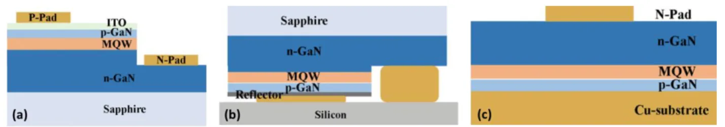
A simplified InGaN/GaN based planar LED structure consists of a GaN buffer layer, n-doped GaN layer followed by the active part composed of InGaN/GaN quantum wells (QWs) and a p-doped GaN layer. The structure is usually grown on sapphire substrates along c-axis. There are three basic LED chip designs that mainly differ by the substrate technology as explained below.16
1. Conventional chip (CC) design: This configuration is realized by etching a part of the LED structure to access the n-GaN such that both n and p electrodes are located at the top as shown in Figure 1.6 (a). A low thickness of moderately resistive p-GaN can limit the current spreading so it is typically covered by a semi-transparent conductive metallization such as Ni/Au. Generally, a transparent electrode of ITO is preferred due to high light absorption by Ni/Au. This design is popular due to its low cost and easy fabrication but it suffers from a poor light extraction and also has a major drawback of poor heat dissipation since sapphire has a low thermal conductivity.
13
2. Flip chip (FC) design: The LED is inverted such that both n and p electrodes are bonded opposite to the sapphire substrate and the whole structure is mounted on a thermally conductive substrate acting as a heat sink for a better heat dissipation (see Figure 1.6 (b)). Alternatively the sapphire substrate can be removed from the top via laser lift off leading to a thin film flip chip (TFFC) design. The exposed n-GaN located at the top allows the freedom to texture or roughen the surface for a better light extraction.17,18
3. Vertical thin film (VTF) design: A third design of LED (see Figure 1.6 (c)) is a vertical structure obtained by flipping the LED structure and removing the native substrate (similar to TFFC design). As the n and p electrodes lie on the opposite side of the structure, the current is injected vertically resulting in a uniform current distribution. A reflective p-contact can be applied on the p-side of the LED chip before bonding it to a metal substrate. This enhances the thermal stability of the LED thanks to the high thermal conductivity of the metal substrate and the reflecting layer at the bottom helps to increase the light extraction.19
1.2.2 Ways to improve light efficiency
The LED performance is usually determined by an external quantum efficiency (EQE) which depends on three main factors as described below:
𝐸𝑄𝐸 = 𝐼𝑄𝐸 × 𝜂𝑒𝑥𝑡× 𝜂𝑖𝑛𝑗 …… (Eq. (1.5)) where IQE is internal quantum efficiency (IQE), ηext is light extraction efficiency and ηinj is
injection efficiency. It is thus important to consider all the above factors to achieve a high wall-plug efficiency in LED structure and different structures have been discussed below to address the same.
Figure 1.6: Three basic designs of an InGaN/GaN planar LED along c-axis: (a) conventional chip (CC),
14
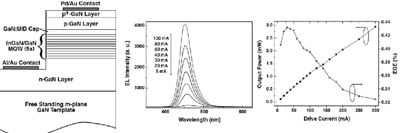
The IQE of an InGaN/GaN LED depends on the crystal quality and structural design of the epitaxial layers. It is generally limited by polarization charges that reduce the radiative recombination inside the structure. As said before, commercial InGaN/GaN based LEDs are commonly grown along polar c-axis involving a high polarization fields along c-axis. This phenomenon reduces the probability of radiative recombination (due to poor overlap of electron and hole wave functions) and can be overcome by the growth of LED structures on non-polar planes such as a-plane and m-plane.11 The growth of non-polar m-plane InGaN/GaN LED on free standing m-plane GaN substrates (see Figure 1.7) has shown an output power of 240 µW at a driving current of 20 mA with an improved heat dissipation.20 Another group has reported a high-power blue-LED on a free-standing (202̅1̅) GaN substrate with a high EQE of 52% and an output power of 30.6 mW at a forward current of 20 mA.21 However, the non-polar GaN substrates with a low defect density are limited as they are expensive, while other available substrates like m-plane SiC or LiAlO2 results in a high density of threading dislocations and stacking faults.22,23
The crossing of high energy electrons over the active region and recombination with the holes present in p-GaN, i.e. the leakage of electrons is commonly observed in InGaN/GaN LEDs and solved by using an electron blocking layer (EBL). A study has been performed on two different structures having a Mg-doped p-type Al0.15Ga0.85N EBL layer: one grown for a c-plane LED on sapphire and other on m-plane GaN substrate. It is observed that with presence of EBL, the c-plane LED exhibit a reduction in efficiency droop by 40% up to a current density of 2250 A/cm2 and m-plane LED nearly retained its efficiency.24 Another work is performed by comparing a standard
Figure 1.7: Schematic of the non-polar m-plane InGaN/GaN based LED grown on free standing m-plane
GaN substrate (left), the EL spectra with increasing current (middle) and the output power and EQE with increasing drive current (right). (Taken from Ref. 20)
15
structure containing an EBL with a constant Al-content 15% to a graded composition EBL (GEBL) with Al composition increasing along the [0001] direction from 0-15%. A reduction of only 4 % in efficiency droop is estimated for the GEBL structure in comparison to 34 % reported for EBL (see Figure 1.8).25 However, later some discrepancy is observed in the use of EBL as some reports demonstrates that the LED structure shows a low EQE with EBL at high current density compared to structure without EBL.26 The simulations performed on different LED structures containing EBL reveal that the role of EBL is actually governed by the Al composition present inside the layer, the band offset ratio and the polarization charges.27,28
Assuming a high value of IQE for a given structure, a poor light extraction can also limit the device efficiency. Due to a high refractive index of GaN (n ≈ 2.5), the angle for the light escape cone is very small and most of the light is totally internally reflected. If we neglect the light coming out from the sides and the back side, only 4 % of light is able to escape from the top surface. In addition the emitted light can reflect onto the substrate and get absorbed by the electrodes after repeated reflections. This issue is overcome by using different methods like surface roughening or texturing techniquesthat can help to scatter the light outwards and avoid the total internal reflection.19,29,30,31 This is done by different methods such as wet etching, laser bombardment or a secondary epitaxial growth. Changing the shape of the LED chip design to hemispherical, quadrilateral, spherical etc. can also help to mitigate the issue.32 The absorption of emitted light by the electrodes and a poor current expansion in p-GaN should also be considered. The contact pads are usually coated with Ni/Au or indium titanium oxide (ITO) thin film. It is reported that Ni/Au films (5 nm/5 nm) and ITO (60 nm) show a transmittance of about 86 % and 98 % for blue light (470 nm).33 Even if the
Figure 1.8: LED structure with EBL: (a) Schematic diagram of the concept of band engineering at EBL
and (b) Normalized efficiency as a function of current density for conventional and GEBL LEDs. (Adapted from Ref. 25).
16
transparency increases with ITO contact, the forward voltage with Ni/Au is lower suggesting good ohmic contact, therefore one has to consider the compromise between light absorption and efficient current injection with the contacts.
Even if a lot of design structures of LED have been explored till date to improve the device efficiency, a decrease in EQE is observed with increasing current density. This so-called “efficiency droop” remains a significant hurdle in the LED technology and is attributed to auger recombination.34 A way to address this issue is to increase the surface area of the LED which will reduce the current density and hence avoid the droop in efficiency. Nanostructured LEDs (such as wires, rods, pyramids…) can be a suitable candidate to serve this purpose (explained in section 1.3.1).
1.2.3 Demonstration of green LEDs
Achieving green emission from InGaN/GaN based LEDs that demands indium-rich InGaN QWs has been made possible only after an intense research work as it involves a lot of serious challenges. The lattice mismatch between GaN and InN is around 11 %. Therefore, as the indium content increases, more and more compressive strain accumulates in InGaN layers. A plastic relaxation can rapidly occur in these layers, which are strongly strained to GaN thereby favoring defect formation such as threading dislocations, stacking faults, etc.35,36 In addition, the low growth temperature required to incorporate high indium content degrades the crystal quality of the active region especially in MOVPE. The defects act as non-radiative centers and reduce the device efficiency. The lattice mismatch also creates a piezoelectric field in the order of MV/cm at the interface of the heterostructures. This leads to the so-called QCSE which can help to red-shift the wavelength emission but the reduced overlapping of electron and hole wave functions will limit the radiative efficiency of the device.
Various types of heterostructures have been reported making use of the band engineering to overcome these issues. Recent work on lattice matched InGaN barriers (with 15 % In-content) instead of conventional GaN barriers in a green LED has shown six-fold increment in the output power with a reduction in efficiency droop.37 The numerical design and analysis of a W-shaped QW has also been currently reported depicted in Figure 1.9 (a) that improved the hole confinement
17
owing to better localization of indium inside QWs. The authors also claim a reduction in defect related to Shockley-Read-Hall (SRH) and Auger recombination rate with the proposed design.38 A three-layer staggered InGaN QWs LED (see Figure 1.9 (b)) exhibits an enhanced radiative recombination rate thanks to the improved electron-hole wave functions overlap design.39 The output power improves by 2-3.5 times when compared to a conventional InGaN/GaN based LED. Another report on graded superlattice (GSL) of AlGaN/GaN has demonstrated a decrease in efficiency droop from 34.9 % to 19.4 % at a current density of 100 A/cm2.40 The GSL structure basically reduces the effective barrier height of the holes, enhancing their injection efficiency as well as polarization fields near the last well. An InGaN based LED with 12-stacked InGaN layer of the GSL is investigated as shown in Figure 1.9 (c) that showed 42.5 % higher output power compared to a conventional LED.41 The report claims that the GSL insertion layer helps to release the residual stress in MQWs and also acts as an electron cooler enhancing the electron capture rate in MQWs. A pre-strained InGaN/GaN layer with 7 % of In-composition is inserted underneath the active InGaN/GaN QWs region showing a remarkable improvement in both the optical and
Figure 1.9: (a) Schematic of the LED structure (at left) and indium composition (on right) of standard
rectangular QWs and W-shaped QWs, adapted from Ref. 38; (b) Output power vs. current density for conventional InGaN QW and three-layer staggered InGaN QW LEDs with the corresponding band energy schematic in the inset, taken from Ref. 39; (c)Schematic of the LED structure with a 12-stacked GSL layer (left) and TEM image of the epitaxial films in the GSL LED (on right), adapted from Ref. 41.
18
electrical properties of the LED.42 The pre-strained layer enables the growth of active QWs at 30 °C higher growth temperature targeting the similar emission wavelength. The growth at relatively higher temperature results in a better crystal quality with improved emission efficiency. Moreover, the power-dependent photoluminescence (PL) measurements showed a reduction in QCSE effect.42
The use of EBL layer to overcome the issue of electron leakage is more challenging while dealing with green emission, due to several reasons: a higher Al content in EBL layer required for green emission increases the polarization mismatch between AlGaN and GaN barriers, the valence-band barrier in EBL is raised affecting the injection of holes into the active region and a high growth temperature required for AlGaN can be detrimental for the quality of the indium rich active region. A lattice-matched InAlN EBL layer has been reported to obtain a better carrier confinement, lesser thermal damage to the active QWs and improved luminous intensity.43 The polarization fields at the interface of the heterostructures can also be addressed by an effective doping profile inside the active region to provide free electrons or holes that can screen the polarization charges at interfaces and reduce the electric field. This involves a p-type or n-type impurity doping inside QWs or barriers. A report on InGaN green LED with Mg-doped barriers has shown 12.4 % reduction in efficiency droop at high current injection.44 Also, it is predicted that the Mg acceptors that are back diffused in the QW close to the p-layer could improve the hole injection efficiency. Similarly, Si-doped barriers in an InGaN green LED with a dopant density of the order of 1020 cm-3 screen the electric field and reduce the roughness at the InGaN/GaN heterostructure interface.45 It also suppresses the local heating and improves the current spreading.
Facing the growth challenges to achieve green emission is also accompanied by an intrinsic difficulty related to thermodynamic instability of InGaN alloys. An uneven distribution of In-composition generally occurs within the film due to the phase separation of In-rich InGaN in its metastable state. It results in a randomness in the potential energy distribution leading to the significant localization of charge carriers.46,47 Theoretical work has shown that the random alloy fluctuations in InGaN alloy contributes to the efficiency droop in InGaN/GaN green LEDs.48 However, other groups have reported the dot-like In-rich InGaN clusters or quantum dots (QDs) act as localized centers that can prevent the carriers to be trapped at the dislocations, reducing the non-radiative recombination.49,50,51 A stable electroluminescence (EL) peak has been reported from
19
InGaN green QDs structure emitting at 527 nm. A negligible shift in the EL peak for current density between 2 to 88 A/cm2 indicates that the QCSE is reduced due to strain relaxation.52 Another work based on coupling of InGaN QW and QD structure has been demonstrated to overcome the small carrier capture cross section provided by the QD and an IQE of 45 % was reported.53
1.3 Moving towards wire-based LEDs
1.3.1 Benefits of wires over planar based LEDs
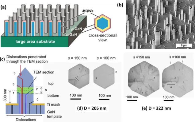
The previous section has described many different issues present in the standard planar c-plane LEDs, such as the high lattice mismatch, the presence of QCSE effect and the high defect density. Nanostructured LEDs have been intensely studied over the past few years as an alternative of planar LEDs. They offer a number of key advantages and have the potential to overcome the limitations of planar LED. The wire growth can be performed either in a self-assembled mode (i.e. wire growth at random positions) or using a patterned mask to achieve organized wires at fixed positions. Both the methods have their own benefits and limitations, which will be described later. The wires are obtained by either a bottom-up approach or a top-down etching. The present thesis is based on radial geometry (i.e. core-shell wires) grown by bottom-up technique as depicted in Figure 1.10 (a).68 This section will be mainly focused on a rapid overview of the state-of-the-art based on this core-shell approach.
The GaN nanowires (NWs) have a high tolerance with different mismatched substrates such as sapphire54,55,56 Si57,58 and graphene59. A typical SEM image of self-assembled GaN wires grown on sapphire substrate demonstrated by our group in 2010 is shown in Figure 1.10 (b).56 The small footprint of the wires reduces the lattice mismatch with the substrate facilitating higher strain relaxation and consequently a decrease of defect density.60,61 The dislocation formation can be avoided in NWs with nm-scaled diameter, while they can be formed for wires having larger diameter at the substrate interface. However, they are mainly found in the immediate vicinity at the wire base and bend to join the lateral free lateral surface.62,63 A detailed study on the growth of highly uniform arrays of GaN nanocolumns with varying diameters on Si substrates is demonstrated by Kishino et al. The dislocations are well filtered at the base of wires and almost
20
terminated at the sidewall for wires with diameter D ≈ 200 nm, while they are observed for wires with D > 200 nm as shown in Figure 1.10 (c-e).62 The low density of dislocations in NW based LED has shown significant improvement in the device performance.64 The core-shell geometry with GaN wires oriented along c-axis allows the QW growth on non-polar m-plane thereby eliminating the QCSE.65 Also a reduction in the value of Auger coefficients by two order of magnitude has been revealed in the core-shell m-plane LED as compared to c-plane planar LED.66
The 3D geometry of wires offers a high surface to volume ratio with respect to the corresponding thin planar film, which significantly increases the total active area emitting light.67 This surface increase allows to reduce the current density for a given carrier injection inside the QWs, thus mitigating the issue of efficiency droop.68 Moreover, the increased active area improves the light extraction in the device allowing a better escape of photons.64 However, the issue of light re-absorption should be considered, which has been commonly reported for core-shell LEDs. Apart
Figure 1.10: (a) Taken from Ref. 68: Schematics of core-shell geometry for InGaN/GaN based LED; (b)
Adapted from Ref. 56.: SEM view of typical self-assembled GaN wires grown on c-plane sapphire substrate; (c-e) Taken from Ref. 62: Schematic diagram of dislocations propagating in a TEM section in (c), magnified plan-view TEM images of nanocolumns with diameters D= 205 nm in (d) and D= 322 nm in (e). Note the nanocolumns are sliced horizontally to a thickness of s at a height of ∼300 nm above their bottoms.
21
from the key benefits mentioned above, the wire based LED also offers a unique functionality of flexibility in a LED device. This will be described later in section 1.4.
1.3.2 Different ways to grow GaN wires
The two main growth techniques to achieve GaN wire growth are namely molecular beam epitaxy (MBE) and MOVPE. The GaN wires are spontaneously grown by MBE in nitrogen-rich conditions with a slow growth rate (≈ 0.6 Å/s) and exhibit a high density (≈ 1010 wires cm-2). They are suitable to produce axial heterostructures. The wire growth by MOVPE requires a control over many growth parameters and exhibits a low wire density (107 wires cm-2) with a faster growth rate (≈ 100 Å/s) and allows growing mainly core-shell heterostructures. A detailed description of GaN wire growth is provided by Nan et al.69 The four growth methods of catalyst-free GaN wires using bottom-up approach by MOVPE are explained below:
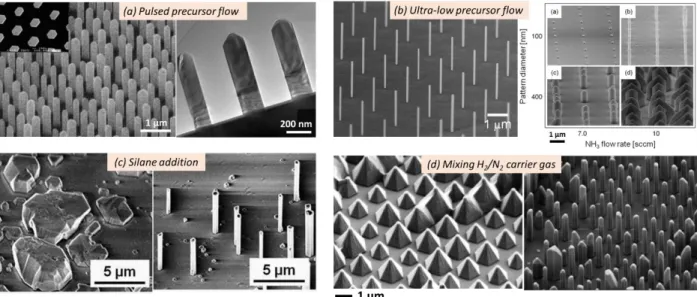
1. The vertical growth of GaN wires along c-axis by using a pulsed growth method has been first reported by Hersee et al. as depicted in Figure 1.11 (a).54 The precursors for Ga and N are alternatively introduced inside the reactor and wires with diameter equal to 221±7 nm are achieved on a patterned Si3N4 mask by selective area growth (SAG). A quite high growth temperature (> 950 °C), high V/III ratio (1500) and low pressure (100-200 mbar) under H2 carrier gas are typically used. This work also served as a milestone for SAG growth establishing a better control over wire dimensions as well as wire density. However, the growth revealed a low growth rate (2 µm/h) and presence of structural defects mainly located at the NW base.54 The growth technique has been later carried out by other groups reporting a high crystal quality of wires.70,71
2. The selective growth of ordered GaN NWs on GaN templates using an ultra-low precursor has been reported by Arakawa’s group demonstrating wires with a diameter of 50 nm (see Figure 1.11 (b)).72 This growth method uses very low TMGa and NH3 flux as (0.1-1.0) µmol/min and (10-100) µmol/min respectively resulting in a V/III ratio between 1 and 50. The growth is performed at high temperature (950-1100 °C), low pressure (100 mbar) using N2 carrier gas without hydrogen dilution. This approach has also been used a little bit earlier in our laboratory to grow GaN wires
22
on bare c-plane sapphire substrates.73 Defect-free wires with excellent optical properties has been reported but with a quite low growth rate (≈ 4 µm/h) that is mainly governed by the wire density. 3. Our group has exploited the strategy of using a high silane flux (200 nmol/min) compared to that for planar growths (10 nmol/min) to favor the vertical growth of very long GaN wires with a growth rate larger than 100 µm/h.56,65 The left and right SEM images in Figure 1.11 (c) shows the wires grown without and with silane respectively. The high silane flux indeed imposes a high n-type doping in the order of 1020 cm-3.74 Other growth parameters fixed during the growth are: high growth temperature (1050 °C), low V/III ratio (<50), high pressure (800 mbar) under high flow of N2 carrier gas. The present thesis work is based on GaN wire growth using the silane approach and more details will be described in Chapter 2.
4. The mixing of H2/N2 carrier gas is another method to achieve GaN wire growth as reported by the group of Waag.75Figure 1.11 (d) shows the selective growth of pyramids on c-sapphire under N2 (on left) but a dilution of the carrier gas with hydrogen having H2/N2 ratio 2:1 allows the formation of m-plane facets (on right). Other growth parameters are similar to that used for the silane approach.
Figure 1.11: Catalyst-free MOVPE methods to grow GaN wires: (a) SEM and TEM images of ordered
GaN wire arrays grown by pulsed precursor mode, adapted from Ref. 54; (b) SEM images of ordered GaN NW array grown by ultra-low precursor flux method as a function of the NH3 flux and the pattern pitch, taken from Ref. 72; (c) SEM images of self-assembled GaN wires grown without (left) and with (right) silane addition, adapted from Ref. 56; (d) SEM images of ordered GaN wire arrays grown without (left) and with (right) hydrogen dilution (2:1) of N2 carrier gas, adapted from Ref. 75.
23
The present work focusses on bottom-up approach only, however some groups have also reported top-down approach to grow wires.76,77 For example, MOCVD grown c-plane GaN on Si templates are etched to fabricate GaN nano rods and this can also be followed by the overgrowth of InGaN shell covering the nano rods to produce core-shell heterostructures.76 Another recent work has reported the fabrication of GaN nanocolumns by etching GaN film on sapphire and followed by lateral overgrowth and annealing.77 Such a hybrid top down approach has shown a reduction in threading dislocation density for the nanocolumns.
1.3.3 Demonstration of MOVPE grown wire based LEDs
NW based LEDs have seen tremendous amount of research over the past few years to gain a deep understanding about the device performance. Many groups have succeeded in fabricating wire LEDs and some companies (GLÖ, Aledia, Osram…) also focus their R&D activity on the same. Before to compete against the planar technology that exhibits highly efficient LED devices, some open issues still remain in the wire LEDs that need to be addressed. A few important works based on core-shell wire LEDs grown by MOVPE will be described in this section and various difficulties are systematically discussed.
1.3.3.1 Early achievement of blue emission
The early demonstration of core-shell NW LED grown by MOCVD has been reported by Lieber
et al.78,79 in 2004 using Ni particles as a catalyst to grow NWs. The catalyst free core-shell m-plane InGaN/GaN based LED has also been demonstrated in our laboratory by Koester et al. in 2011 exhibiting an emission around 410 nm.65 The radial m-plane QWs are present only around the upper part of the GaN wire covered by the p-GaN shell while the wire-bottom is heavily n-doped. This unique structure can allow an efficient way to access the p-GaN top) and n-GaN (wire-bottom) for electrical contacts. This work has been further extended by fabricating a single NW LED using the core-shell InGaN/GaN wire containing five radial QWs.80 Later, the group of Ra in 2013 has also described a wire-based LED grown with the help of Au catalyst using a pulsed-precursor flow.81 The radial QWs are grown on the non-polar and semi-polar planes under a reduced growth pressure. An EQE of 27.9 % has been estimated for a current injection of 50 mA.81
24
The EL spectra reveals an emission at 440 nm, which is considered to originate mainly from the
m-plane sidewall QWs.
A color shift in the EL spectra has usually been reported in NW LEDs as a function of applied voltage. It is mentioned by Koester et al.65 that the QWs are present on both the lateral m-plane facet as well as the top c-plane facet with different thicknesses and In-content. A change in the EL color emission is recorded and explained by a competition between the carrier injection in the axial and the radial QWs. Similarly, a color shift has been reported for LEDs based on organized array of nanostructures.82,83,85,86
A work by Hong et al.82 has shown a monolithic LED with GaN nanorod array grown using SiO2 mask on GaN template on sapphire substrate with a height of about 520 nm. The indium content in InxGa(1-x)N QWs present on the topmost and sidewall facets and estimated by EDX is found to be x ≈ 0.6 and ≈ 0.15 respectively. The light emission is observed to be tunable from 690 nm to double peak (500 and 440 nm) by adjusting the voltage bias from 3 to 10 V. A field distribution model is used to explain the change in EL color. The carriers are injected preferentially in the tip due to flat
Figure 1.12: Adapted from Ref. 83- (a) Bright field STEM image of core-shell GaN microrod with arrows
indicating the layers containing aluminum, (b) STEM-CL peak wavelength mapping of the core-shell rod, (c) Optical microscope image of the chip layout (top image), electroluminescence images from the LED chip at 2 mA (right image) & 10 mA (image below) and (d) EQE and wall-plug efficiency of the blue LED with the current density.
25
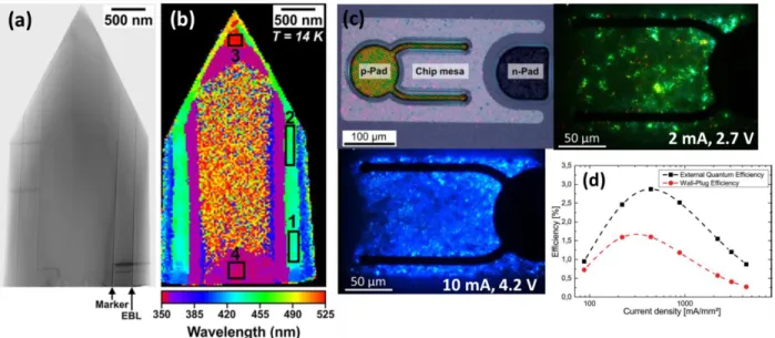
equipotential surface, which changed to a curved shape as the applied voltage bias increases allowing the carriers to enter though m-plane sidewall QWs. The temperature-dependent photoluminescence (PL) spectra reveal an IQE of 32±8 %. Another study conducted by OSRAM is based on organized array of GaN microrod (MR) LED grown on n-doped c-plane GaN template on sapphire wafers.83 A SiO
x mask layer fabricated by photolithography is used to grow uniform wires with a height of 3 µm. The presence of single QW on semi-polar and non-polar facets is confirmed by STEM-CL measurements (see Figure 1.12), while the estimated IQE from PL experiment is 10 %. A shift from green luminescence at low bias (arising from semi-polar facets) to blue luminescence for voltage > 3.0 V (coming from non-polar m-plane facets) is reported. The estimated EQE of the LED is 3 % at a current density of 400 mA/mm2. Beyond the fabrication and demonstration of blue emission, white light emission has also been reported from microrod LED in this work and will be discussed in the next section.
The color switching observed in the above-mentioned reports is further investigated by the GLÖ-company.84,85 The organized core-shell NW LEDs are fabricated with a silicon nitride mask patterned by nanoimprint on n-type GaN/sapphire substrate. The LED contains single QW located at the non-polar m-plane and the junction of semi-polar and m-plane. An electrical model is proposed to explain the color shift observed in a single NW LED. A network of diodes connected in parallel is used to represent a core-shell NW where the current distribution is calculated for different applied voltage biases and different configuration for contacts. It is concluded that the In-rich segments are injected at low bias, while the parallel and radial shell resistances dominate at higher biases allowing the current injection in the m-plane QW with low In content.
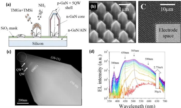
Recently the group of Amano has demonstrated a multi-band emission covering almost the whole visible region using core-shell InGaN/GaN nanorods grown on patterned substrates as shown in Figure 1.13.86 It is explained that the incorporation kinetics for indium on the different planes of 3D nano-structures is different. So apart from the growth conditions, the size, pitch, and angle of a top cone of the NRs array also play a major role for the QW homogeneity. The PL spectra reveals the presence of different contributions arising from different parts of the NR. The NRs are then used to fabricate a LED device by filling the space between the rods by spin-on-glass (SOG) to prevent the electron leakage and ITO was used as a top contact. A thin film of Ti/Al is used as a
26
back contact that can be seen in the SEM image in Figure 1.13 (labelled by ‘electrode space’). The measured EL spectra is observed to strongly depend on the current density and is explained by a similar transportation mechanism of charge carriers as reported previously by other groups mentioned above.
The multi-color emission or the color tuning with applied voltage bias in NW based LED could be used for a full color display application, however it is important to control the color emission while targeting a narrow band single color emitting device. A work by Chen et al.87 has demonstrated GaN nanorod LED array grown on SiO2 mask with a height of 1.3 µm with InGaN QWs located on both lateral sidewall as well the nanorod top as described in Figure 1.14. The TEM observation reveals a poor structural quality of the top QWs. A transparent GaZnO of low resistivity is deposited using MBE to form a coalesced layer on the nanorods to improve the current spreading over the m-plane QWs. A stable EL spectrum is recorded centered at 463 nm with no significant shift unlike the above mentioned reports. However, a large turn-on voltage around 6 V is recorded.
Figure 1.13: Taken from Ref. 86- (a)Schematics of the InGaN/GaN SAG nanorod containing n-GaN core, 5 InGaN QWs & a p-GaN shell observed with the SEM images shown in (b), (c) STEM image of the core-shell layers structure and (d) Room-temperature EL spectra recorded at different injection currents.
27
Apart from these reports, the highest IQE of 62 % has been reported till date for core-wire based LED by Nami et al. to the best of our knowledge.88 The high-performance core-shell InGaN/GaN wire-based LEDs are grown on patterned SiNx mask with an improved p-GaN growth. The EQE was measured at 8.3 % without any device packaging, although the shift of the EL emission with changing applied bias is also reported in this work.
1.3.3.2 Achieving white LEDs using phosphors
The realization of LEDs using core-shell m-plane InGaN/GaN wires grown by MOCVD has been mainly demonstrated for blue emission. Longer wavelength emissions like green, yellow and red with stable color at varying bias voltage still remain a challenge for this core-shell geometry due to the difficulty to increase the In incorporation on the m-plane surface. This makes the RGB (red/green/blue) approach difficult to achieve white light emission from InGaN/GaN wire based LEDs. Another key solution to address this issue is to down convert the blue light from these LEDs using phosphors emitting at different colors. A phosphor is a material that absorbs light of a given energy and emits light having lower energy. Intensive research based on their synthesis
optimization offers different phosphors with high efficiency (η) such
as RbLi(Li3SiO4)2:Eu2+ (RLSO:Eu2+) emitting green (η≈80%)89, Ce,Gd:Y3Al5O12
Figure 1.14: Adapted from Ref. 87- (a) SEM image of the nanorod LED array at large magnification, (b)
TEM image of a nanorod LED NR with magnified TEM images corresponding to differernt portions of the QWs such as top face (in pink), left and right-sidewall QWs near the top (in red & green resp.) and left-sidewall QW near the bottom (in blue) with a high- resolution TEM image of the three left-sidewall QW and (c) EL spectra when injection current density increasing from 16 to 224 A/cm2 with inset showing the photograph of LED at current density of 224 A/cm2.
![Figure 2.7: (Adapted from Ref. 14) Atom probe tomography measurements. (a) 3D reconstruction of the In-atom distribution in a wire slice, oriented along the [0001] zone axis but tilted to show the non-uniform In-distribution within the QW planes, (b) 2D](https://thumb-eu.123doks.com/thumbv2/123doknet/14503134.719635/66.918.179.768.554.878/figure-adapted-tomography-measurements-reconstruction-distribution-oriented-distribution.webp)