Domain and lattice contributions to dielectric and
piezoelectric properties of Pb(Zr
x,Ti
1−x)O
3thin films as a
function of composition
S. Hiboux, P. Muralt, and T. Maeder
Laboratoire de Ce´ramique, Federal Institute of Technology (EPFL), CH-1015 Lausanne, Switzerland
(Received 29 December 1998; accepted 28 July 1999)
In situ reactively sputter deposited, 300-nm-thick Pb(Zrx,Ti1−x)O3 thin films were investigated as a function of composition, texture, and different electrodes (Pt,RuO2). X-ray diffraction analysis, ferroelectric, dielectric, and piezoelectric measurements were carried out. While for dielectric properties bulklike contributions from lattice as well as from domains are observed, domain wall contributions to piezoelectric properties are very much reduced in the morphotropic phase boundary (MPB) region. Permittivity and d33do not peak at the same composition; the MPB region is
broadened up and generally shifted to the tetragonal side.
I. INTRODUCTION
Ferroelectric thin films of the solid solution Pb(Zrx,Ti1−x)O3(PZT) find a growing interest for
appli-cations in nonvolatile memories,1,2microactuators,3and infrared detectors.4,5As known from bulk ceramics, the properties vary substantially with the compositional parameter x. There is still a lack of knowledge on how properties change as a function of composition in thin films. The most complete work performed to date is the investigation of metalorganic chemical vapor deposition (MOCVD) grown single-crystalline, (100)-oriented PZT films by Foster et al.,6 covering film morphology,
mi-crostructure data, refractive index, dielectric constant, ferroelectric polarization, and coercive field. Piezoelec-tric properties are not included in this study. In addition, polycrystalline films are more relevant for applications than single-crystal films. They may differ in properties, since domain contributions depend on grain size and mi-crostructure.7,8Apart from application driven interests to
find optimal compositions for polycrystalline PZT films,9 the variation of concentration may also help to gain a better comprehension of the mechanisms govern-ing PZT thin film properties. The region near the mor-photropic phase boundary (MPB), i.e., x near 0.5, is of special interest. This boundary separates the tetragonal symmetry of Ti-rich compositions from the rhombohe-dral symmetry of Zr-rich compositions. The large num-ber of possible polarization directions at this boundary leads to a peaking of permittivity and piezoelectric co-efficients. In bulk PZT this occurs at x⳱ 0.50 to 0.52.10 Thin films may behave differently in their domain con-tributions, because of the clamping to the substrate and smaller grains and because of the columnar, often tex-tured microstructure.
It is the scope of the paper to investigate polycrystal-line PZT films throughout the compositional range of the solid solution, to characterize also piezoelectric proper-ties, and to address the question of domain contributions. The compositional parameter x (Zr content) was varied between 0.1 and 0.7 in steps of 0.05–0.1. One set of samples consisted of (111)-textured films on platinum electrodes. A second set of samples was grown on RuO2
electrodes. The PZT thin flims of this set exhibit a more or less random orientation.
II. THIN FILM DEPOSITION
PZT thin films were deposited by dynamic in situ sput-tering from three elemental targets.11–13 The Ti and Zr
magnetrons were operated with direct-current (dc) power, and the Pb magnetron with radio-frequency (rf ) power. The films were grown at 570 °C with a dynamic rate of 3 nm/min, corresponding to about one unit cell per turn of the substrate carrier. The temperature had been previously calibrated with thermocouples. The applied process parameters are given in Table I.
Silicon wafers covered by 1m of thermal oxide were utilized as substrates. Two types of bottom electrodes were applied. The (111)-oriented growth was achieved by means of TiO2/Pt /TiO2electrodes. The lower
10-nm-thick TiO2film served as adhesion layer. It was actually
composed of an in situ postannealed Ti layer followed by a sputtered TiO2layer. The 2-nm-thick top film served as
seeding layer for (111)-oriented grains.14 The 100-nm-thick platinum film was well (111) textured. The second type of electrode consisted of a randomly textured, 300-nm-thick RuO2film on a TiO2adhesion layer. Samples
of both electrodes were coated in each PZT run. Platinum top electrodes were sputter deposited at room tempera-ture through mechanical masks with round holes of 0.6-mm diameter. Film thickness was controlled by power/ time regulation and measured by profilometry (Tencor Alphastep) at chemically etched steps.
The variation of composition was obtained by varying the powers of the Ti and Zr sources. The individual depo-sition rates for ZrO2 and TiO2 films were previously determined at the sputter conditions of the PZT process. The molecular flux ratio of these oxides during the PZT process has been taken as nominal Zr to Ti ratio [Zr]/[Ti] of the PZT thin film. The lead stoichiometry was ob-tained by the self-stabilization of the process. Excess lead was reevaporated.11 For this work, the applied PbO flux was twice as high as the sum of the ZrO2 and
TiO2 fluxes.
III. CHARACTERIZATION
A. Compositional and structural characterization A chemical analysis of PZT thin films on RuO2 (Pt
electrodes are less suited as Pb and Pt lines coincide) was carried out by energy dispersive spectroscopy (EDS), to-gether with electron microscopy (Philips XL30), and by x-ray fluorescence (XRF) in a Kevex XRF analyzer. For the compositional range between 10 and 55% Zr content on the B-site (compositional parameter x defined as x⳱ [Zr]/([Zr] + [Ti]), both types of measurements (see Fig. 1) yielded a good correspondence between the nomi-nal ratio of Zr to Ti cation concentrations, as defined by the ZrO2 to TiO2flux ratio, and the measured [Zr]/[Ti] ratio. At higher concentration, a significant deviation was observed. This indicates either an increased desorption of Zr or a decreased desorption of Ti. A nominal value of 70% Zr content (i.e., x⳱ [Zr]/([Zr] + [Ti]) ⳱ 0.7) cor-responds to a real concentration of rather 60%. In what follows, the nominal value is always indicated as composition.
Film morphology was studied by means of scanning electron microscopy (Philips XL30). The average size of the grains decreased with increasing Zr content from
200 nm at x⳱ 0.1 to 100 nm at x ⳱ 0.7. The nontextured samples showed a more rough and irregular grain mor-phology than the (111)-textured layers grown on plati-num. The latter exhibited remarkably homogeneous grain sizes at Zr-rich compositions [see Figs. 2(a) and 2(b)].
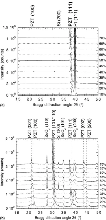
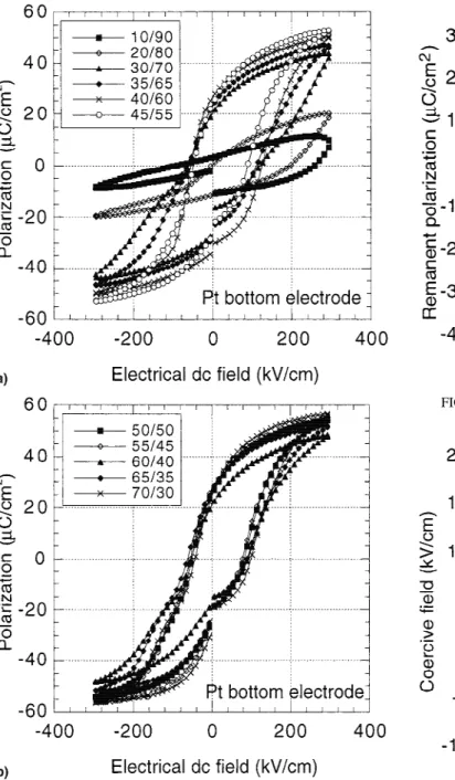
Film crystallinity and orientation were studied using standard –2 x-ray diffraction (XRD). Figure 3 shows the x-ray diffraction patterns for PZT on Pt and RuO2as
a function of the composition (from 10 to 70% of Zr). On Pt(111) the films show a high degree of (111) orientation, whereas on the randomly oriented RuO2 bottom elec-trode a random orientation is obtained. No second phases, and especially no pyrochlore, are observed.
The lattice constants a and c of the tetragonal films were extracted from the first-order Bragg peaks (100) and (001), as well as from the second-order Bragg peaks (200) and (002). Whereas the (100) and (200) reflections yield the same a within small limits of ±0.02 Å, the extraction of c is problematic in the compositional range from 30% to 40% [see Fig. 4(a)]. The {00h} peaks are broader and less intense than the {h00} peaks. For this reason the (001) and (002) peak positions are probably shifted toward the (100) and (200) peaks. Nevertheless, the tetragonality is lower than in bulk ceramics, espe-cially in the range from x⳱ 0.3 to 0.5. At x ⳱ 0.45 no tetragonal splitting is observed. However, the {h00} peaks are still broadened at x⳱ 0.45, as compared to the peaks at x ⳱ 0.50. This allows to conclude that the morphotropic phase boundary is near x⳱ 0.45 (nominal composition), instead of x⳱ 0.52 as in a bulk ceramic. The concentration measurements suggest that the real Zr concentration at the MPB is even lower, i.e., between TABLE I. Sputter parameters of the PZT deposition process.
Parameters General conditions
x⳱ [Zr]/([Zr] + [Ti]) from 0.1 to 0.7
Lead power supply rf 150 W
Titanium power supply dc from 450 to 150 W Zirconium power supply dc from 32 to 224 W Working pressure 16 mtorr pure O2(20 sccm)
Dynamic deposition rate 3 nm/min
Distance targets–substrate 50 mm
Deposition temperature 570 °C
Cooling down 80 mtorr of O2/1 h
FIG. 1. Chemical analysis of the Zr/Ti ratio in the PZT thin films obtained by XRF and EDS.
x⳱ 0.42 and 0.44. Another difference in bulk ceramics
was observed in the spacings of (111) planes (⳱d111). These differ considerably from bulk values in the te-tragonal part of compositions [see Fig. 4(b)]. The jump at the morphotropic phase boundary is absent. In contrast, bulk and thin film data are in better agreement at rhom-bohedral compositions. Thin film data are, however, con-sistent. The (111) plane spacings from films on Pt(111), from films on RuO2, and calculated spacings from the a
and c parameters of Fig. 4(a) are the same within the experimental errors. The lattice constant a of the rhom-bohedral compositions is generally found to be higher in thin films than in bulk ceramics.6,15Our data confirm this tendency. Lattice defects6 and stresses are thought to cause this shift.15
The tetragonal distortion is also manifested in the line broadening of higher order x-ray Bragg peaks. Such line broadening of higher order peaks is ascribed to strain variations.16 With b
hkl ⳱ (dhkl)
−1 and ␦b
hkl ⳱ cos/ ⭈ 2␦hkl, where 2␦hkl means the full width at
half-maximum (FWHM), a strain variation of ±␦S is evaluated according to the following formula:
␦S=1⁄ 2
冉
共␦s222兲 2− 共␦s111兲 2 s222 2− s111 2冊
1Ⲑ2 .The result of this evaluation is shown in Fig. 5, together with the thin film tetragonality parameter (a −
c)/a. The strain variation clearly increases with
tetrago-nality and amounts to about 20% of the (theoretical) spontaneous strain. The behavior as a function of com-position indicates that the tetragonal phase exists in the range 0 艋 x < 0.4, since in this range a nearly linear increase of ␦S with the spontaneous tetragonal strain is observed. Between 0.4 and 0.5 there is a plateau followed by a drop at compositions with rhombohedral symmetry. FIG. 2. SEM pictures of PZT thin films with different Zr/Ti ratios: (a)
on Pt bottom electrode, (b) on RuO2bottom electrode.
FIG. 3. X-ray–2 scans for each of the PZT compositions: (a) PZT thin films on platinum electrodes, yielding a dominant (111)-orientation, (b) random PZT thin films on RuO2electrodes.
B. Ferroelectric and dielectric characterization Dielectric properties were measured with a HP 4284A impedance analyzer. The polarization was determined with a Sawer-Tower bridge (RT66A of Radiant Tech-nologies). The piezoelectric coefficient d33 was
deter-mined with the help of an extremely sensitive double side interferometer described in Refs. 17 and 18.
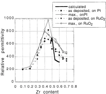
The polarization loops were performed with a 100 Hz triangular signal. Figures 6(a) and 6(b) show the polari-zation hysteresis loops of PZT on Pt as a function of the Zr/Ti ratio. The same measurements have also been made with PZT on RuO2 bottom electrodes, showing similar
behavior. At low Zr concentrations (x ⳱ 0.1 and x ⳱ 0.2) only partial switching occurs because the coercive field is too large. This is brought to the fore by the piezoelectric measurements presented later. For x > 0.2, the polarization curves show a normal ferroelectric be-havior. A negative prepolarization of the films together with a positive voltage shift are observed. Prepolarization and internal bias field will be quantified and discussed later in the context of d33measurement.
Remanent polarizations and coercive fields have been extracted from the polarization curves. They are shown in Figs. 7 and 8 as a function of composition. Note that the values at x ⳱ 0.1 and x ⳱ 0.2 do not represent real properties, as no complete switching was achieved.
The remanent polarization increases up to x⳱ 0.4, to reach a value close to 30C/cm2on Pt and 25 C/cm2 on RuO2. Negative values are higher than positive ones.
For higher Zr concentrations, the values remain constant, except for x⳱ 0.6 on Pt, where Prdrops to 20C/cm
2
. The remanent polarization is higher for PZT on Pt bot-tom electrodes. As for the coercive field, it can be clearly seen that positive values are higher than the negative ones, indicating a negative internal bias field. The mini-mum coercive field occurs at x⳱ 0.50 to 0.55. Lower Ec
values were achieved on Pt bottom electrodes, confirm-ing again superior properties on this electrode.
FIG. 4. (a) Lattice constants a and c (tetragonal symmetry) and a (rhombohedral symmetry) derived from {n00} reflections of the PZT/ RuO2series as a function of composition. The bulk data shown for
comparison have been taken from Ref. 31. Lattice spacing between (111) planes, as obtained from (111) Bragg peak positions of x-ray
–2 scans, compared to calculated values derived from the lattice
constants [Fig. 4(a)] and bulk data.31
FIG. 5. Strain variation, as derived from the widening of the recipro-cal lattice vectors, as a function of composition. The tetragonality parameter (c − a)/a derived from {n00} reflections of the PZT/RuO2
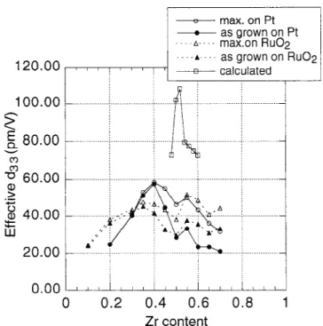
The relative permittivity was measured as a function of an applied dc bias field (CV curve). The dc field was varied between ±300 kV/cm in steps of 1.5 kV/cm at a speed of 1 step/s. The alternating current (ac) field had an amplitude of 5 kV/cm and a frequency of 5 kHz. Figure 9 shows the results as a function of the composition for the case of the PZT/Pt films.
The field dependence of the dielectric constant reflects the contribution of domain walls, which contribute through their oscillation amplitude as well as their den-sity. A peaking occurs near the coercive field due to a
high domain wall density. Upon application of a larger field, domain contributions are reduced as the number of domain walls decreases and as the oscillation amplitudes decrease. In case of low Zr concentrations (x⳱ 0.1 and 0.2) there is practically no domain contribution. From
x⳱ 0.3, the “butterfly” symmetric loops are observed. We
can see the increase and then the decrease of the permit-tivity with the composition, with a maxima for x⳱ 0.45. The same tendency is obtained for PZT on RuO2but with a maxima for x⳱ 0.40. Permittivity measurements thus confirm XRD results and indicate that MPB position at
x⳱ 0.4–0.45. Figure 10 shows zero-field (Edc⳱ 0) and
FIG. 6. Polarization hysteresis loops of the PZT films grown on Pt electrodes: (a) the tetragonal side of the composition range, (b) the rhombohedral side of the composition range.
FIG. 7. Remanent polarization as a function of composition.
FIG. 8. Coercive field as a function of composition (from polarization measurements).
maximum (Edc ⳱ Ec) values as a function of the com-position and the bottom electrode. As in the case of a bulk ceramic,19we can observe a peak for the permittiv-ity. The films grown on platinum electrodes exhibit higher values. Zero-field values are of the same order than for an unpoled ceramic (⑀ ⳱ 800 for PZT on Pt). The maximum permittivity is obtained when the dc field is close to the coercive one. This increase can reach 20%. The behavior is the same on RuO2, except that the
maxi-mum value is lower (700 at the unpoled virgin state). For comparison with bulk values, one has to keep in mind that bulk data are measured for constant stress (KT33) or
constant strain (KS33). In case of a thin film on a much
thicker substrate, none of these cases applies. The bound-ary conditions are mixed: constant stress perpendicular to the film plane and constant strain in the film plane. With a complete set of materials coefficients, as published by Berlincourt, Cmolik, and Jaffe,19a hypothetical thin film dielectric constant can be calculated as the following:
K33, f=K33 T − 2d31 2 共s11 E + s12 E兲 0 .
The obtained values are depicted in Fig. 10 for com-parison. At maximum, the zero-field values are very close or somewhat higher to the so calculated K33, f. The
peak is, however, much broader and shifted to tetragonal compositions.
C. Piezoelectric coefficientd33
The piezoelectric d33coefficient has been measured as small signal response to a small ac field as a function of a much larger dc field. The same parameters were ap-plied as for the permittivity measurements, i.e., 5 kHz, 5kV/cm, 1.5 kV/cm steps, and 1 step/s. Figures 11(a) and 11(b) show the d33 hysteresis loops of PZT on RuO2,
versus composition. Same measurments have been made on Pt bottom electrode. With such measurements self-poling by the process can be detected, because a nonzero
d33means also a nonzero polarization.
For 10% Zr, the switching of domains is incomplete; i.e., the transition through zero polarization is not achieved. The film is strongly negatively polarized. For
x⳱ 0.2, more but still uncomplete switching is observed.
This observation is in agreement with the other electrical FIG. 9. Relative permittivity for PZT on Pt: (a) the tetragonal side of
the composition range, (b) the rhombohedral side of the composition range.
FIG. 10. As-grown (virgin) and maximum relative permittivities as a function of composition. The calculated curve describes the bulk ce-ramic data,19corrected for the clamping effect.
results seen before. For x⳱ 0.3 and higher, the hyster-esis loops indicate complete switching, i.e., a normal behavior of a ferroelectric material. However, negative initial values and thus poling by the process are still observed. Figure 12 represents the initial (at the virgin state) and maximum (measured at negative field) d33 values, as a function of the composition. It is known that thin film values are reduced with respect to bulk ceramic values because of the clamping to the substrate. The cor-rection can be calculated as follows:20
d33, f=d33− 2s13 E s11 E + s12 E d31 .
This thin film value d33, f, which has been calculated
from ceramics data,10is also given in Fig. 12.
The measured values are smaller than expected. On Pt electrodes, d33 increases with x on the
tetrago-nal side, reaches a maximum for x ⳱ 0.4 (60 pm/V), and decreases on the rhombohedric side. On RuO2,
the behavior is quite the same, but the curve is flatter. On this bottom electrode, the values are lower around the maximum area, whereas, for the compositions near PT and PZ, they are higher. A strong similarity can be observed between the initial (virgin) and the maximum values, for each composition. Under x < 0.4, maximum values are very close to the initial ones. For x > 0.4, initial values are a little bit lower. On Pt electrodes, the maximum is obtained for x ⳱ 0.4 (in contrast with 0.45 for the permittivity). Once again, the peak in properties is shifted toward Ti richer compositions.
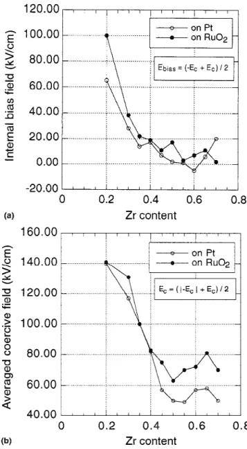
On the basis of these d33 measurements, true values for internal and coercive field (slow loop) can be re-ported [Figs. 13(a) and 13(b)], since—in contrast to hysteresis measurements—the zero polarization state can be located. On both bottom electrodes, high values are observed for tetragonal compositions (for
x ⳱ 0.1 the value is too high to be measurable). The
minimum is located between x ⳱ 0.5 and 0.6, the val-ues of PZT/Pt being somewhat smaller than the ones of PZT/RuO2.
FIG. 11. Effective piezoelectric coefficient d33,ffor PZT on RuO2: (a) the tetragonal side of the composition range, (b) the rhombohedral side of the composition range.
FIG. 12. As-grown (virgin) and maximum of the effective d33
piezo-electric coefficient of the PZT films grown on Pt and RuO2. The
calculated curve describes the available bulk ceramic data,19corrected
IV. DISCUSSION
A. Lattice and domain contributions
One of the distinct features of ferroelectrics is the fact that dielectric and piezoelectric responses originate from two different mechanisms: first there is a lattice contri-bution from the displacements of the individual ions (in-trinsic contribution) and second there is a contribution from domain wall motions (extrinsic contribution). The latter contribution depends very much on the density and mobility of domain walls. When the small signal re-sponse is measured, i.e., the first harmonic to a small alternating electric field, the reversible part of domain wall oscillations is contributing only. The domain wall oscillates so to speak in the bottom of a potential well.
The domain contribution varies with a (much stronger) superimposed dc field. The maximal contribution occurs around the coercive field at the maximal density of do-main walls. At high dc fields, the dodo-main wall density is reduced very much and the overall polarization tends toward saturation. The domain contribution is approach-ing zero, and the lattice contribution is dominatapproach-ing. This is similar to freezing out domain wall oscillations by cooling, as was done for bulk ceramics.21
Whereas all domain wall oscillations due to Eacshow up in the dielectric response, only the ones that change strains influence the piezoelectric response. A displace-ment of a 180° domain wall does not modify the strains and thus yields no piezoelectric response. In case of (111)-oriented tetragonal films, even 90° walls should not contribute, as all domains exhibit the same spacing between (111) planes in the stress-free case. We indeed observed that domain wall contributions are very much smaller in the piezoelectric than in the dielectric sponse. Figure 14 shows a comparison of the two re-sponses for (111)-PZT on platinum as a function of composition. It is evident that the permittivity is very much enhanced by the ferroelectric domain wall motions. The total permittivity achieves values similar to bulk ceramic permittivities. At maximum, the lattice contrib-utes a quarter of the value (250 of 1000). This is in good agreement with low-temperature measurements of bulk ceramics PZT.22There is, however, less agreement in the case of the d33 coefficient. In our (111) thin films the
lattice contributes with 66% to the peak value, whereas in bulk ceramics this contribution amounts to 40% only.22 In addition, the intrinsic contribution is reduced near the MPB and enhanced at the other compositions as com-pared to bulk ceramics (taking into account an approxi-mate reduction for the clamping). No pronounced peaking of the lattice contribution is observed. Since our films are (111)-oriented, one would expect no domain contribution at compositions with tetragonal symmetry. Their peaking at 35 – 45% indicates that they nevertheless exist. Either the rhombohedral symmetry is still partially present at these compositions or oscillating 90° domain walls between up and down domains somehow couple to strains. This cannot be excluded as there is a tilt angle between the (111)-planes of such neighboring domains. In thin films, such tilting is impossible near the electrode interface. The resulting stresses may yield strains that change the spacing between (111)-planes. Such inhomo-geneous strain was shown to exist in the previous section (Fig. 5). Their correlation with tetragonality indicates that the strain inhomogeneity is mostly due to spontane-ous strains. Comparison between permittivity and d33
leads thus to the conclusion that 180° domain wall os-cillations contribute very much to the dielectric constant and show maximum activity at the 45/55 composition. Domain wall oscillations coupling to strains are very FIG. 13. (a) Internal bias field and (b) averaged coercive field as
much reduced with respect to bulk ceramics and show a maximum activity at the 40/60 composition. This shift of piezoelectric activity in direction of tetragonal composi-tions was recently also observed for the e31coefficient.9 The random PZT films on RuO2 electrodes show an
even more reduced domain wall contribution. The lattice contribution is about the same. The clamping of domain walls is thus more effective on RuO2. In intrinsic
prop-erties, the two types of PZT thin films do not differ significantly. The effective electrostrictive coefficient
Qeff, as defined by the equation d33⳱ 2K33⑀0QeffP3, has
been evaluated for the lattice contributions. For all films,
Qeffvaries between 0.025 and 0.04 m 4
C−2.
The reduction of piezoelectrically active domain wall motions in thin films may have several origins. It was shown for bulk ceramics that domain wall mobility and configuration depend very much on the microstructure of the PZT.8 Below a grain size of 1 m, domains are
smaller and charged domain walls are more likely to appear. Furthermore, for small grains, the density of do-mains increases and so their mobility is reduced. Thin films of PZT predominantly consist of such small grains, at least in less than 1-m-thick films (the size of the grains in our 300-nm-thick films is less or equal to 300 nm). It has also been shown23that 1m was the critical
thickness below which piezoelectric properties de-creased. Further evidence of property reduction is given by the fact that the tetragonality is reduced in the com-positional range between 0.3 and 0.5. It is known from BaTiO3 ceramics
7
that small grains (<1 m) have a reduced tetragonality and even show the appearance of an orthorhombic phase. In case of PZT, the critical thick-ness is rather in the 100-nm size. The clamping to the substrate may inhibit domain wall motions, too. Epitaxial ordering of the PZT lattice on top of the electrode is established in the paraelectric phase. The strong aniso-tropic stresses imposed by the ferroelectric phase transi-tion might be released partially by dislocatransi-tions and other defects, which freeze-in the domain pattern at the inter-face. Alternatively, nano-sized domain patterns might be imposed by the electrode in order to limit strains in the electrode material. Finally, films obtained by physical vapor deposition (PVD) techniques might exhibit a larger amount of oxygen vacancies. These may compensate charges at domain walls, or polarization charges near the interface, during cool down between ferroelectric phase transition and room temperature. The fact that RuO2and Pt electrodes lead to different lattice contributions sug-gests that phenomena at the interface are very crucial.
B. Internal bias field
A pronounced feature of our sputter deposited films is the occurrence of strong internal bias fields, or voltage offsets, which are particularly strong for Ti-rich compo-sitions [see Fig. 13(a)]. This phenomenon has been ob-served by several groups in case of sputter-deposited films,24,25in plasma-treated films (RIE-etching),26and in
the case of different materials for top and bottom elec-trodes.27Except for the latter case, which is explained by differences in the work function of the two metals, such voltage shift is related to nonuniformly distributed oxy-gen vacancies,27 the formation of dipoles with oxygen vacancies and negatively charged acceptors,28or also the nonuniform compensation of oxygen vacancies.24 The creation of oxygen vacancies is due to vacuum exposi-FIG. 14. (a) Permittivity and (b) d33of PZT/Pt films as a function
of composition, showing the contributions of lattice and domains ef-fects (the lattice contribution corresponds to the high-field value at 300 kV/cm).
tion at high temperatures, plasma self-bias during etching, and acceptor doping. The finding of Prokopalo29 that the probability of oxygen vacancies increases with the Ti content is in fact compatible with experiments presented in this paper. This effect results in a clamping of the domain walls, which acts against domain motion. In addition to voltage shifts, pinning by space charges at the interfaces leads also to a slanting of the hysteresis loop by screening domains from reorientation.26 The
theory of creation of an internal bias field by oxygen vacancies is compatible with our fabrication process, since the sputtered PZT films are grown in situ in a low oxygen partial pressure. All these phenomena are indeed in good accordance with the properties we have meas-ured in our films: the coercive field, the voltage off-set, and the slanting of the hysteresis loop increase with increasing Ti concentration for concentrations higher than 60%. The role of oxygen vacancies is further sup-ported by the fact that postannealing in oxygen was in-creasing dielectric and piezoelectric properties, while at the same time the internal bias field and the built-in polarization were reduced (details will be published later).
On the RuO2 bottom electrode, the tendency is the
same as that on Pt, but the internal bias field is higher on this electrode. This effect can be explained by the asym-metry of the electrical contacts (the top electrode is al-ways Pt), which yields a difference in the built-in voltages at the two different interfaces.
C. Coercive field
Figure 15 shows the positive, negative, and averaged coercive fields, taken from polarization, dielectric, and piezoelectric measurements. Similar to the internal bias field, the coercive fields decreases with increasing Zr. This tendency is also observed in PZT thin films by Foster,6 Takayama,25 and Hector.15 Compared to bulk ceramics, coercive fields are much higher in thin films. This effect may be due to the same reasons as described above for the internal bias field, i.e., clamping of do-mains by dipolar or charged defects, large stresses in the film, and small grain sizes. One can see that the different methods for measuring Ecyield different results. When
Ec is derived from the polarization loop, which is cap-tured within 10 ms, transient phenomena influence the experiment. In contrast, coercive fields derived from C-V curvelike measurements (thus permittivity and d33) re-flect a quasi-static situation. There is nevertheless a dif-ference between Ec(⑀33) and Ec(d33): at the first field the domain density is maximal; at the second field the aver-age polarization is zero. Our measurement shows that the maximal domain wall density is achieved before the av-erage polarization has reached zero. The dynamic Ec
from polarization loops is generally larger than the two
other ones. However, for Ti-rich compositions a too low value is obtained due to strong backswitching of domains.
D. Phase transitions
There is evidence from dielectric and piezoelectric properties as well as from XRD data that the MPB is shifted toward the tetragonal side by 5–10%. Previous studies performed so far with epitaxial films6,25and by polycrystalline sol-gel films15confirmed the usual MPB FIG. 15. Coercive fields from small signal response measurements (d33permittivity) and from the polarization hysteresis loops. In (a) the
positive and negative values are shown; in (b) the averaged values are shown.
composition within a precision of 5%. These studies, however, did not include piezoelectric properties, which apparently are more sensitive to microstructural features than dielectric properties. A recent study on sol-gel-processed PZT thin films revealed that the effective pi-ezoelectric coefficient e31,f was peaking at lower Zr
concentrations (i.e., at x⳱ 0.45) than the permittivity or
d33,f(i.e., at 53/47).9The evaluation of intrinsic and
ex-trinsic contributions (see Fig. 14) shows that inex-trinsic contributions peak at x ⳱ 0.40, whereas the strongest extrinsic contributions are seen in the dielectric response at x⳱ 0.45. This contribution is most likely due to 180° domain wall motions, because otherwise it should also be seen in the piezoelectric response. In the latter, the ex-trinsic contribution is equal for x⳱ 0.4 and x ⳱ 0.45. The origin of the different positions of the peaks lies thus in different composition dependencies of intrinsic and the various extrinsic contributions.
One particular behavior we have also observed in our thin films is the presence of a second peak in d33and K33
appearing at x ⳱ 0.55 for extrinsic and x ⳱ 0.60 for intrinsic contributions (see Fig. 14), which, to our knowl-edge was never observed before. These compositions come quite close to the normal MPB compositions when taking into account the compositional correction. It could be that our films exhibit a morphotropic phase boundary region which is very much extended as compared to large grain materials. Instead of one peak, two peaks would appear. Alternatively, the second peak could be due to the transition between the high-temperature and low-temperature rhombohedric phase, which would lead to improved properties because of multiple cell contribu-tions in this phase.10 More investigations are needed to clarify the origin of this second peak.
Independently of the open origin of the second peak it is clear that the phase transition at the morphotropic phase boundary (RH-T) is broadened. The peak of the dielectric constant is much wider than in bulk ceramics, a reduction of tetragonality occurs, and piezoelectric properties are reduced inside the MPB region. The in-trinsic properties, such as the electrostrictive coefficient, are, however, relatively uniform as a function of compo-sition. There is thus a large reduction of piezoelectrically active domain wall motions in the MPB zone. This is understandable for (111)-oriented films in the tetragonal phase. However, the random oriented films on RuO2
show that this explanation does not hold, as these films show even less domain activity than the (111) films on platinum. One is thus left with the possibility that the interface to the bottom electrode plays the major role. During nucleation of the film, this interface has a major influence on the final grains size. The elastic and plastic properties and the thermal expansion coefficients of the electrode materials should have a major influence on how 90° domain patterns accommodate the electrode. In
addition, the ability to neutralize charged domain walls may play a role too. The broadening of the MPB transi-tion and the reductransi-tion of 90° domain wall motransi-tions can thus be understood as a combination of the effects of small grains, large stresses (mostly inhomogeneous) due to impossible stress relaxation at the interface, and pin-ning of domain walls by defect.
The role of the average stress is not as important (measured about 100 MPa tensile at 45/55 composition). However, the strain variation yields much more local stresses of several 100 MPa up to a few GPa, taking into account a biaxial of modulus of about 100 GPa. Piezo-electric couplings between order parameter (i.e., the po-larization components P1, P2, and P3) and shear stress components X4, X5, and X6 (crystal frame) may yield a broadening of the transition. This coupling is written in the crystal frame as follows (see e.g., Ref. 30):
−Q44[X4P2P3 + X5P1P3+ X6P1P2] .
For the (111) textured films, this coupling term leads also to couplings with nonshear stress components de-fined in the film frame. A uniform film stressf in the
plane of the film leads to the following piezoelectric coupling term:
1⁄3Q
44[P2P3+ P1P3+ P1P2]f .
Q44 is positive and quite large. A compressive stress
thus would stabilize the solution P1⳱ P2⳱ P3, thus the
rhombohedric case. Tensile stress stabilizes other rhom-bohedric solutions (P1 ⳱ P2 ⳱ −P3) or new solutions
with two P-components different from zero and one zero (orthorhombic). The coupling to stress may also account for the shift of the phase transition. One may argue that the local stress that develops due to clamping and the ferroelectric phase transition always opposes the increase of the tetragonal c axis along the in-plane directions, thus increasing the free energy of the tetragonal solution for all orientations. The difference from thicker films pre-pared by sol-gel techniques, where no shift of MPB is observed (more precisely, d33 and K33 do not show a shift, but the e31peak is shifted to the tetragonal side9),
is possibly a more relaxed film/Pt interface and a larger grains size.
V. CONCLUSION
Pb(Zrx,Ti1−x)O3thin films have been deposited by in
situ reactive sputtering. The obtained films do not
con-tain second phases. The compositional parameter was varied between 0.1 and 0.7. Two series of 300-nm-thick films have been fabricated. One consisted of (111)-textured films on platinum electrodes, the other of ran-domly oriented films on RuO2 electrodes. The
permittivity is measured to be as high as in bulk ceram-ics, while a strong reduction in d33 is observed, even
when taking into account the clamping by the substrate. Small signal response measurements as a function of the dc electrical field allowed one to separate lattice and domain wall contributions. It is the domain wall contri-bution which is very much reduced in the case of piezo-electric properties, while for dipiezo-electric properties bulklike contributions are observed. This allows one to conclude that the piezoelectrically active 90° domains are hindered in their motion or do not exist as abundantly as in large-grained bulk ceramics. As a further conse-quence, the maximum dielectric and piezoelectric re-sponses are not found at the same Zr contents. The latter is shifted by ⌬x ⳱ −0.05 toward tetragonal composi-tions. The morphotropic phase boundary is found to be shifted toward tetragonal compositions. X-ray line width measurements indicate a broadened transition zone be-tween x ⳱ 0.40 and 0.50. They also reveal large inho-mogeneous strains, which increase with increasing tetragonality. These strains result mainly from the clamp-ing to the electrode.
Coercive field and voltage shift increase strongly with increasing Ti content or tetragonality. The growing in-homogeneous strains might be one reason for that. On the other hand, the ability to form oxygen vacancies in-creases also with a higher Ti content. The lowering of coercive field and voltage shift by annealing in oxygen suggests indeed that domain pinning by oxygen defects play an important role. A third important parameter is the grain size, as known from literature on bulk ceramics. With an average diameter of 150 nm at MPB composi-tions, the grain size is critical; i.e., domain configurations are limited to laminar structures with limited possibility to relax stresses.
The main difference between the two series is the smaller domain wall contributions in films grown on RuO2. The lattice contribution to piezoelectricity are about equal. A puzzling point was discovered in (111)-oriented PZT thin films on platinum. For tetragonal sym-metry, 90° domains should be equivalent with respect to strains in the [111] direction. However, they show a larger domain wall contribution than the random films on RuO2. The influence of the electrodes and the symme-tries present in the widened MPB region need to be clari-fied in future work.
ACKNOWLEDGMENT
This work was supported by the Swiss Priority Pro-gram on Materials Research (PPM).
REFERENCES
1. C.A. Araujo, L.D. MacMillan, B.M. Melnick, J.D. Cuchiaro, and J.F. Scott, Ferroelectrics 104, 241 (1990).
2. R.E. Jones, P. Zu¨rcher, P. Chou, D.J. Taylor, Y.T. Lii, B. Jiang, P.D. Maniar, and S.J. Gillespie, Microelectron. Eng. 29, 3 (1995).
3. P. Muralt, M. Kohli, T. Maeder, A. Kholkin, K.G. Brooks, N. Set-ter, and R. Luthier, Sens. Actuators A 48, 157 (1995).
4. R. Bruchhaus, Ferroelectrics 133, 73 (1992).
5. M. Kohli, C. Wu¨thrich, K.G. Brooks, B. Willing, M. Forster, P. Muralt, N. Setter, and P. Ryser, Sens. Actuators A 60, 147 (1997).
6. C.M. Foster, G-R. Bai, R. Csencsits, J. Vetrone, R. Jammy, L.A. Wills, E. Carr, and J. Amano, J. Appl. Phys. 81, 2349 (1997). 7. G. Arlt, D. Hennings, and G. de Witt, J. Appl. Phys. 58, 1619
(1985).
8. G. Arlt, Ferroelectrics 91, 3 (1989).
9. M-A. Dubois, P. Muralt, D.V. Taylor, and S. Hiboux, Integr. Fer-roelectr. 22, 535 (1998).
10. B. Jaffe, W.R. Cook, and H. Jaffe, Piezoelectric Ceramics (Aca-demic Press, London, 1971).
11. T. Maeder, P. Muralt, M. Kohli, A. Kholkin, and N. Setter, Br. Ceram. Proc. 54, 206 (1995).
12. T. Maeder and P. Muralt, in Epitaxial Oxide Thin Films and
Het-erostructures, edited by D.K. Fork, J.M. Phillips, R. Ramesh, and
R.M. Wolf (Mater. Res. Soc. Symp. Proc. 341, Pittsburgh, PA, 1994), pp. 361–366.
13. R. Bruchhaus, H. Huber, D. Peitzer, and W. Wersing, Integr. Fer-roelectr. 2, 157 (1992).
14. P. Muralt, T. Maeder, L. Sagalowicz, S. Hiboux, S. Scalese, D. Naumovic, R.G. Agostino, N. Xanthopoulos, H.J. Mathieu, L. Patthey, and E.L. Bullock. J. Appl. Phys. 83, 3835 (1998). 15. H. Hector, N. Floquet, J.C. Niepce, P. Gaucher, and J.P. Ganne,
Microelectron. Eng. 29, 285 (1995).
16. B.E. Warren and B.I. Auerbach, J. Appl. Phys. 21, 595 (1950). 17. A. Kholkin, E. Colla, K. Brooks, P. Muralt, M. Kohli, T. Maeder,
D. Taylor, and N. Setter, Microelectron. Eng. 29, 261 (1995). 18. A.L. Kholkin, Ch. Wu¨thrich, D.V. Taylor, and N. Setter, Rev. Sci.
Instrum. 67, 1935 (1996).
19. D.A. Berlincourt, C. Cmolik, and H. Jaffe, Proceedings of the IRE (Institute of Radio Engineers, New York, 1960), Vol. 48, pp. 220–229.
20. K. Lefki and G.J.M. Dormans, J. Appl. Phys. 76, 1764 (1994). 21. X.L. Zhang, Z.X. Chen, L.E. Cross, and W.A. Schulze, J. Mater.
Sci. 18, 968 (1983).
22. Z.Q. Zhuang, M.J. Haun, S-J. Jang, and L.E. Cross, IEEE Trans. UFFC 36, 413 (1989).
23. S. Trolier-McKinstry, P. Aungkavattana, F. Chu, J. Lacey, J-P. Maria, J.F. Shepard, Jr., T. Su, and F. Xu, in Ferroelectric
Thin Films VI, edited by R.E. Treece, R.E. Jones, C.M. Forster,
S.B. Desu, and I.K. Yoo (Mater. Res. Soc. Symp. Proc. 493, Pittsburgh, PA, 1998), pp. 59–68.
24. G.E. Pike, W.L. Warren, D. Dimos, B.A. Tuttle, R. Ramesh, J. Lee, V.G. Keramidas, and J.T. Evans, Appl. Phys. Lett. 66, 484 (1995).
25. R. Takayama and Y. Tomita, J. Appl. Phys. 65, 1666 (1989). 26. E.G. Lee, D.J. Wouters, G. Willems, and H.E. Maes, Appl. Phys.
Lett. 70, 2404 (1997).
27. J. Lee, C.H. Choi, B.H. Park, T.W. Noh, and J.K. Lee, Appl. Phys. Lett. 72, 3380 (1998).
28. K. Carl and K.H. Ha¨rdtl, Ferroelectrics 17, 473 (1978). 29. O.I. Prokopalo, Sov. Phys. Solid State 21, 1768 (1980). 30. M.J. Haun, E. Furmann, S.J. Jang, and L.E. Cross, Ferroelectrics
99, 13 (1989).
31. V.V. Eremkin, V.G. Smotrakov, and E.G. Fesenko, Ferroelectrics 110, 137 (1990).