Selective GAS sensor based on screen-printed ZNO nanorods
Texte intégral
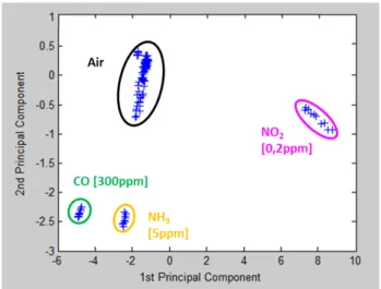
Figure
Documents relatifs
The fabrication of sensors and solid oxide fuel cell (SOFC) modules in microtechnology is particularly challenging since high operating temperatures of several hundred degrees
The evaporation of the ethylene glycol leaves a layer of ZnO which constitutes the sensing layer of the sensor (as it is shown in fig. Design of used sensing cells : a) design of
L’id´ ee principale est de construire des algorithmes ` a partitionnement adaptatif qui divisent successivement l’espace de recherche en plusieurs sous r´ egions, en se basant pour
Elle attendait, elle ne savait quoi mais elle attendait… Elle se sentait glisser dans une sorte de vide, comme si dans un premier temps, elle s’abandonnait à elle-même
Les infections ostéo-articulaires chez l’enfant: Etude retrospective à l’hôpital d’Enfants de
This study demonstrates a new electrochemical method for rapid determination of ascorbic acid in real samples with electrochemically pretreated screen-printed carbon
The dependence of films properties including structure, microstructure as well as optical on deposition parameters (deposition temperature and sputtering pressure) are
are developing the Screen Printing technique for depositing a single layer quarter wavelength thick antireflection coating of titanium dioxide on silicon substrate.. The ink is
