HAL Id: hal-00365408
https://hal.archives-ouvertes.fr/hal-00365408
Preprint submitted on 3 Mar 2009
HAL is a multi-disciplinary open access
archive for the deposit and dissemination of
sci-entific research documents, whether they are
pub-lished or not. The documents may come from
teaching and research institutions in France or
abroad, or from public or private research centers.
L’archive ouverte pluridisciplinaire HAL, est
destinée au dépôt et à la diffusion de documents
scientifiques de niveau recherche, publiés ou non,
émanant des établissements d’enseignement et de
recherche français ou étrangers, des laboratoires
publics ou privés.
Photon correlation spectroscopy on a single quantum
dot embedded in a nanowire
Gregory Sallen, Adrien Tribu, Thomas Aichele, Régis André, Catherine
Bougerol, Serge Tatarenko, Kuntheak Kheng, Jean-Philippe Poizat
To cite this version:
Gregory Sallen, Adrien Tribu, Thomas Aichele, Régis André, Catherine Bougerol, et al.. Photon
correlation spectroscopy on a single quantum dot embedded in a nanowire. 2009. �hal-00365408�
G. Sallen1, A. Tribu2, T. Aichele1, R. Andr´e1, C. Bougerol1, S. Tatarenko1, K. Kheng2, and J. Ph. Poizat1 CEA-CNRS-UJF group ’Nanophysique et Semiconducteurs’,
1
Institut N´eel, CNRS - Universit´e Joseph Fourier, 38042 Grenoble, France,
2
CEA/INAC/SP2M, 38054 Grenoble, France
We have observed strong photoluminescence from a single CdSe quantum dot embedded in a ZnSe nanowire. Exciton, biexciton and charged exciton lines have been identified unambiguously using photon correlation spectroscopy. This technique has provided a detailed picture of the dynamics of this new system. This type of semi conducting quantum dot turns out to be a very efficient single photon source in the visible. Its particular growth technique opens new possibilities as compared to the usual self-asssembled quantum dots.
PACS numbers: 78.67.Lt, 78.55.Et
Semiconductor nanowires (NWs) appear as promising building blocks for nanoscale devices and circuits with impressive potential applications including nanoelectron-ics [1, 2, 3], optoelectronnanoelectron-ics (light emitting diodes [4, 5], nanolasers [6]), thermoelectrical energy conversion [7], and biological or chemical sensors [8]. Moreover, high quality defect free nanowires can be grown on low-cost, routinely used substrates such as silicon, which means that they could easily be used for fabricating commer-cial devices and could possibly be integrated with main-stream Si microelectronics devices.
NW growth methods allow for the variation of the chemical composition [9, 10] or doping [11] along the lon-gitudinal or radial directions. This enables the fabrica-tion of well controlled 1D nanoscale heterostructures [10]. For example, as shown in this work, it is possible to in-sert a slice of a low band gap semiconductor within a high bandgap NW and thus realize a light emitting quantum dot (QD) operating as a single photon source [12, 13]. So far, work on the light emitting properties of single quantum dots has mainly concerned self-assembled QDs formed by surface forces induced by lattice mismatch be-tween different materials. Such QDs have been widely used in the past decade as single photon sources [14] and for their potential application in quantum information processing (see for example [15, 16]). QDs in NWs appear to be an interesting alternative to self-assembled quan-tum dots. The absence of a wetting layer offers a better confinement which could enable room temperature pro-duction of single photons [13]. Radial growth techniques enable engineering of optical guides allowing more effi-cient light extraction than in bulk materials [17, 18]. Fur-thermore, NW based heterostructures, being much less limited by lattice mismatches, greatly widen the possible materials combinations and enable well controlled stack-ing of several QDs in a sstack-ingle NW, offerstack-ing intereststack-ing possibilities for quantum information processing [19].
In this letter we present the first detailed optical char-acterization of excitonic emission in a single CdSe QD embedded in a ZnSe NW. We have already shown that this system is an efficient single photon source operat-ing at temperature as high as 220 K [13]. Soperat-ingle
pho-Figure 1: Scanning electron microscope image of a single CdSe/ZnSe nanowire deposited on a silicon substrate.
ton emission from NWs has otherwise only been demon-strated at 4 K in InAs QDs embedded in InP NWs [12]. Our system emits light around 550 nm (2.2eV) where silicon avalanche photodiodes (APDs) are very efficient. This has allowed us to perform the first thorough spec-troscopic analysis of a QD embedded in a NW by using photon correlation spectroscopy [20]. We have identi-fied unambiguously the exciton, biexciton, and charged exciton lines and obtained information on the charging dynamics of this QD.
The wires are grown by Molecular Beam Epitaxy (MBE) in the Vapour-Liquid-Solid (VLS) growth mode catalysed by gold particles on a Si substrate. In order to make QDs, a small region of CdSe is inserted in the ZnSe NW. This is done by interrupting the ZnSe growth, changing to CdSe growth for a short time and then grow-ing ZnSe again [13]. Details about the growth of the ZnSe NWs can be found in reference [21]. The wire diameter (around 10 nm) is of the order of the bulk exciton Bohr diameter for CdSe (11 nm). This means that the carri-ers in the CdSe QD are in the strong quantum confine-ment regime. For the study of single NWs, the sample is sonicated in methanol, causing NWs to break off the substrate into the solution. Droplets of this solution are then deposited on a Si substrate, and a low density of individual NWs is obtained after evaporation. As shown in fig. 1, individual NWs can be isolated, allowing single QD optical spectroscopy.
The experimental apparatus is a standard micropho-toluminescence (µPL) set-up. The samples are mounted on a XYZ piezo motor system in a He flow cryostat at
2 a temperature of 4 K. The optical excitation is provided
by a 405 nm continuous-wave (CW) diode laser illuminat-ing the sample via a microscope objective of numerical aperture N A = 0.65 located in the cryostat. The NW emission is collected by the same objective and sent to a 50/50 beamsplitter for correlation measurements. In each arm of the beamsplitter, the light is dispersed by a monochromator (1200 grooves/mm grating, 30 cm and 50 cm focal length respectively). Each monochromator has a switchable mirror inside, which can direct the lumines-cence either onto a charge coupled device (CCD) camera for the measurement of the PL spectrum or through the exit slit towards a low jitter (40 ps), high quantum effi-ciency APD. The detectors send electrical pulses into a time-correlated single photon module that builts an his-togram of the time delays between successive photons. This histogram is proportional to the second order cor-relation function g(2)(t) [14]. The overall temporal
res-olution of our set-up is essentially limited by the jitter of the APDs and the dispersion of the monochromator gratings. This time resolution was measured by record-ing the autocorrelation function of 1 ps pulses from a frequency-doubled Ti:Sapphire laser. A full width at half maximum of 90 ps was obtained for the autocorrelation function peak.
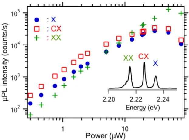
The results presented in this work all come from the same QD. A typical µPL spectrum is shown in the inset of fig. 2 where three lines can be seen. A comparison with relative energy positions of known emission lines in spectra of self-assembled CdSe/ZnSe QDs [22, 23] sug-gests that these lines correspond to the exciton (X), the biexciton (XX) and the charged exciton (CX). Unam-biguous proof for the assignement of these lines will be given below using photon correlation spectroscopy. The width of the lines is due to spectral diffusion [24].
One of the characteristic features of such NW QD structures is their polarization properties. As shown in [13] the excitation efficiency and the luminescence are both strongly polarization dependent [25, 26, 27]. A 90% contrast is obtained for the excitation efficiency de-pending on the direction of the linear polarization of the pumping laser. The light emission is also 90% linearly polarized in the same direction as the best pumping po-larization, independently of the excitation polarization.
It can be seen in fig. 2 that the saturation level of the XX line is more than three times larger than that of the X line. This is due to a strong storage effect of the dark exciton state owing to a rather large dark-bright exciton splitting (∆E = 6 meV) [28]. The dark exciton state reduces the intensity of the X line owing to the leakage from the bright to the dark exciton states caused by spin flip but it remains an efficient intermediate state for populating the XX state [29].
The level scheme used to model our system is shown in figure 3. It is based on models used in references [30, 31, 32] where the carriers can enter the QD either individually (power dependent rates γC1and γC2) or
al-ready bound as excitons (power dependent rate r). We
102 103 104 105 µPL intensity (counts/s) 1 10 Power (µW) : X : CX : XX 30 20 10 0 x10 3 2.24 2.22 2.20 Energy (eV) X XX CX
Figure 2: Inset : µPL spectrum at an excitation power of P = 15µW . The electronic background noise has been subtracted. Main plot : Line intensities as a function of excitation power.
Figure 3: Level scheme including the empty dot (E0), the
dark exciton (EXD), the bright exciton (EXB), the
biexci-ton (EX X), the charged dot (EC), and the charged exciton
(ECX). The various rates between the different level are
in-dicated in the figure.
have added the dark exciton, which plays a key role in our system. It includes the bright and dark exciton, the charged exciton, and the biexciton. A triexciton level and a charged biexciton level are also included to avoid artificial saturation of the biexciton and of the charged exciton but they are not represented in figure 3.
All of the power independent parameters of the model can be evaluated independently prior to photon corre-lation experiments by performing lifetime measurements [28]. Their values are listed in table I. These values are compatible with what has already been measured on self-assembled CdSe/ZnSe QDs [23].
We come now to the main results of this work on
pho-γX γX X γCX γSP1 γSP2 γN R
1.4 2.5 1.7 1.4 0 0.2
1.5 1.0 0.5 0.0 g (2) X (t) 60 50 40 30 20 10 0 Coincidences (a) 6 5 4 3 2 1 0 g (2) X-XX (t) -4 -2 0 2 4 t (ns) 200 150 100 50 0 Coincidences (b)
Figure 4: (a) Exciton emission autocorrelation, (b) exciton-biexciton cross-correlation for an excitation power P = 15µW . The left axes are the correlation functions corrected from the background and the right axes are the raw coinci-dence rates (see text). The fit is performed using the model based on fig. 3. The power dependent parameters used for the fit are r = 0.6ns−1, γC1 = γC2 = 1ns−1. The other
parameters are given in table I.
ton correlation experiments. We present first the data concerning the neutral QD in fig. 4. The autocorrelation of the X line emission is shown in fig. 4 (a) exhibiting a clear antibunching which is characteristic of the statistics of a single photon emitter [14].
Fig 4 (b) shows the cross correlation measurement be-tween the X and the XX line. It displays the typical asymmetric shape with bunching and antibunching fea-tures that is the signature for the cascaded emission of a XX photon followed by a X photon [33]. This allows us to identify unambiguously these two lines as exciton and biexciton of the same QD. Note that the narrow bunch-ing peak can only be fitted if the dark exciton is included in the model.
For all the correlation graphs (figs. 4 and 5) the right vertical axes are the raw number of coincidences. The left axes represent the normalized correlation function according to a Poisson statistics where the coincidences involving background photons have been subtracted. The corrected correlation function g(2) is related to the
un-corrected one gu(2) by g(2) − 1 = (g
(2)
u − 1)/ρ2, where ρ = S/(S + B) with S and B respectively the number of signal and background photons as measured in the spec-trum of fig. 2.
The autocorrelation of the CX line is shown in fig. 5 (a). As for the X line, it exhibits a clear antibunching.
1.5 1.0 0.5 0.0 g (2) CX (t) 100 80 60 40 20 0 Coincidences 1.5 1.0 0.5 0.0 g (2) X-CX (t) -8 -4 0 4 8 t (ns) 60 40 20 0 Coincidences (a) (b)
Figure 5: (a) Charged exciton autocorrelation for an exci-tation power P = 8µW , (b) Exciton-Charged exciton cross-correlation for an excitation power P = 10µW . The fits are performed using the model based on fig. 3. The power de-pendent parameters used for the fits are respectively r = 0.31ns−1, γC1 = 0.09ns−1, γC2 = 0.058ns−1 for the CX
autocorrelation (a) and r = 0.37ns−1, γC1 = 0.25ns−1,
γC2 = 0.28ns− 1
for the X-CX cross-correlation (b). The other parameters are given in table I. (c) Representation of the stream of photons coming alternatively from the neutral and the charged QD.
Also, on a larger time scale, a bunching effect can be ob-served. This is due to the hopping from the charged state to the neutral state of the QD as confirmed by the X-CX cross correlation displayed in fig. 5 (b). This proves that the CX line comes from the same QD as the X line. The situation is depicted schematically in fig. 5 (c), which shows that the photons are emitted either from the charged or from the neutral state of the QD. The average time spent by the quantum dot in the charged state is given by the characteristic time of an exponential fitting of the bunching peak in fig. 5 (a) which is 5 ns. It should be noticed that the antibunching dip in figure 5 (b) is not symmetrical. Negative (positive) time corre-sponds to the probability of detecting a CX (X) photon after having detected a X (CX) photon. Formation of a CX in an empty QD (t < 0) requires the loading of three charges, whereas the formation of an X in a QD with a single charge (level Ecin fig. 3) is faster since it requires
only the loading of a single charge (t > 0) [30, 31, 32]. Note that we do not know whether this charge is positive or negative. We can only say that by comparison with
4 spectra for self-assembled CdSe/ZnSe QDs [22, 23] the
charge state is probably negative.
As can be seen in figs. 4 and 5 the experimental results are fitted very well by the model shown in fig.3 taking into account the temporal resolution of our experimental set-up (90 ps). Inclusion of the dark exciton turned out to be essential for the modelling of the photon correlation data. Allowing for the coexistence of two excitation mecha-nisms, namely charge by charge (described by γC1 and
γC2) or directly feeding the QD with an already bound
exciton (described by r) has also turned out to be neces-sary for the fitting. The QD charge hopping time depends on the value of these parameters. Note that XX autocor-relation and the CX-XX cross-corautocor-relation (not shown) are also fitted well using the same set of parameters [24]. The model gives also the correct intensities of the spec-tral lines within 10% [24].
In conclusion, we have used photon correlation spec-troscopy to characterize a new type of light emitting quantum dot embedded in a nanowire. We obtained a very good fit to the experimental data with a model based on a standard excitonic level scheme. This allowed
us to extract quite complete dynamics of the neutral and charged excitons including charge hopping between these two states of the QD. CdSe/ZnSe QDs in NWs are nano-objects situated between self-assembled QDs and CdSe based colloidal nanocrystals [34, 35]. The latter operate at room temperature but have a blinking problem and a lifetime above 20 ns. On the other hand, self-assembled QDs are non-blinking and feature a sub-nanosecond life-time allowing GHz repetition rates. QDs embedded in NWs have the potential to combine the best of both worlds by offering non-blinking room temperature [13] single photon sources with a high repetition rate. Fur-thermore, the versatility of this particular nanostructure growth technique offers interesting perspectives for en-gineering semi-conducting QDs, such as coupled QDs or waveguide coupled QDs.
We thank L. Besombes for many fruitful discussions, F. Donatini for very efficient technical support, and R. Cox for a careful reading of the manuscript. T.A. acknowl-edges support by Deutscher Akademischer Austauschdi-enst (DAAD). Part of this work was supported by Euro-pean project QAP (Contract No. 15848).
[1] X. Duan, Y. Huang, Y. Cui, J. Wang, C. M. Lieber, Nature 409, 66 (2001)
[2] W. Lu, C. M. Lieber, Nature Materials 6, 841 (2007) [3] C. Thelander, T. Martensson, M. T. Bj¨ork, B. J. Ohlsson,
M. W. Larsson, L. R. Wallenberg, L. Samuelson, Appl. Phys. Lett. 83, 2052, (2003).
[4] R. K¨onenkamp, Robert C. Word, C. Schlegel Appl. Phys. Lett. 85, 6004 (2004)
[5] H.M. Kim, Y.H. Cho, H. Lee, S.I. Kim, S.R. Ryu, D.Y. Kim, T.W. Kang, K.S. Chung, Nano Lett. 4, 1059 (2004) [6] X. Duan, Y. Huang, R. Agarwal, and C. M. Lieber,
Na-ture 421, 241 (2003)
[7] A.I. Hochbaum, R.Chen, R.D. Delgado, W. Liang, E.C. Garnett, M. Najarian, A. Majumdar, P. Yang, Nature 451, 163 (2008)
[8] Y. Cui, Q. Wei, H. Park, C. M. Lieber, Science 293, 1289 (2001)
[9] M. S. Gudiksen, L. Lauhon, J. Wang, D. C. Smith, C. M. Lieber, Nature 415, 617 (2002)
[10] M. T. Bj¨ork, B. J. Ohlsson, T. Sass, A. I. Persson, C. Thelander, M. H. Magnusson, K. Deppert, L. R. Wal-lenberg, L. Samuelson, Nanoletters 2, 87 (2002); Appl. Phys. Lett. 80, 1058 (2002)
[11] C. Yang, Z. Zhong, C. M. Lieber, Science 310, 1304 (2005)
[12] M. T. Borgstr¨om, V. Zwiller, E. M¨uller, A. Imamoglu, Nano Lett. 5, 1439 (2005)
[13] A. Tribu, G. Sallen, T. Aichele, R Andr´e, J.-Ph. Poizat, C. Bougerol, S. Tatarenko, K. Kheng, Nano Lett. 8, 4326 (2008)
[14] P. Michler, A. Kiraz, C. Becher, W.V. Schoenfeld, P.M. Petroff, L. Zhang, E. Hu, A. Imamoglu, Science 290, 2282 (2000).
[15] I. Fushman, D. Englund, A. Faraon, N. Stoltz, P. Petroff, J. Vu˘ckovic, Science 320, 769 (2008)
[16] R. Hanson, D.D. Awschalom, Nature 453, 1043 (2008) [17] P.J. Pauzauskie, P. Yang, Materials Today 9, 36 (2006) [18] N. Gregersen, T.R. Nielsen, J. Claudon, J.M. G´erard, J.
Mørk, Opt. Lett. 33, 1693 (2008)
[19] C. Simon, Y.M. Niquet, X. Caillet, J. Eymery, J.P. Poizat, J.M. G´erard Phys. Rev. B 75, 081302 (2007) [20] A. Kiraz, S. F¨aith, C. Becher, B. Gayral, W.V.
Schoen-feld, P.M. Petroff, Lidong Zhang, E. Hu, A. Imamoˇglu, Phys. Rev. B 65, 161303(R) (2002).
[21] T. Aichele, A. Tribu, C. Bougerol, K. Kheng, R. Andr´e, S. Tatarenko Appl. Phys. Lett. 93, 143106 (2008) [22] V. T¨urck, S. Rodt, R. Heitz, O. Stier, M. Strassburg,
U. W. Pohl, D. Bimberg, Phys. Status Solidi b 224, 217 (2001)
[23] B. Patton, W. Langbein, U. Woggon, Phys. Rev. B 68, 125316 (2003)
[24] G. Sallen, PhD thesis, Universit´e Joseph Fourier, Grenoble (2009). http://tel.archives-ouvertes.fr/tel-00362497/fr/
[25] J. Wang, M.S. Gudiksen, X. Duan, Y. Cui, C.M. Lieber, Science, 293, 1455 (2001).
[26] Y.M. Niquet, D. Camacho Mojica, Phys. Rev. B 77, 115316 (2008).
[27] M. H. M. van Weert et al, arXiv:0808.2908
[28] G. Sallen, A. Tribu, T. Aichele, R. Andr´e, L. Besombes, C. Bougerol, S. Tatarenko, K. Kheng, J. Ph. Poizat, arXiv:0903.0497
[29] M. Reischle, G. J. Beirne, R. Roßbach, M. Jetter, P. Michler Phys. Rev. Lett. 101, 146402 (2008)
[30] C. Santori, D. Fattal, J. Vuˇckovi´c, G. S. Solomon, E. Waks, Y. Yamamoto Phys. Rev. B 69, 205324 (2004) [31] M. H. Baier, A. Malko, E. Pelucchi, D. Y. Oberli, E.
Kapon, Phys. Rev. B 73, 205321 (2006)
[32] J. Suffczy´nski, T. Kazimierczuk, M. Goryca, B. Piechal, A. Trajnerowicz, K. Kowalik, P. Kossacki, A. Golnik, K.
P. Korona, M. Nawrocki, J. A. Gaj, G. Karczewski, Phys. Rev. B 74, 085319 (2006)
[33] E. Moreau, I. Robert, L. Manin, V. Thierry-Mieg, J. M. G´erard, I. Abram, Phys. Rev. Lett. 87, 183601 (2001). [34] P. Michler, A. Imamoglu, M.D. Mason, P.J. Carson, G.F.
Strouse, S.K. Buratto, Nature 406, 968 (2000)
[35] B. Mahler, P. Spinicelli, S. Buil, X. Quelin, J.P. Hermier, B. Dubertet, Nature Materials 7, 659 (2008)