HAL Id: tel-00647310
https://tel.archives-ouvertes.fr/tel-00647310
Submitted on 1 Dec 2011HAL is a multi-disciplinary open access archive for the deposit and dissemination of sci-entific research documents, whether they are pub-lished or not. The documents may come from teaching and research institutions in France or abroad, or from public or private research centers.
L’archive ouverte pluridisciplinaire HAL, est destinée au dépôt et à la diffusion de documents scientifiques de niveau recherche, publiés ou non, émanant des établissements d’enseignement et de recherche français ou étrangers, des laboratoires publics ou privés.
Injection de spin dans le germanium : de l’injecteur
ferromagnétique métallique à l’injecteur semiconducteur
(Ge,Mn)
Abhinav Jain
To cite this version:
Abhinav Jain. Injection de spin dans le germanium : de l’injecteur ferromagnétique métallique à l’injecteur semiconducteur (Ge,Mn). Autre [cond-mat.other]. Université de Grenoble, 2011. Français. �NNT : 2011GRENY049�. �tel-00647310�
THÈSE
Pour obtenir le grade de
DOCTEUR DE L’UNIVERSITÉ DE GRENOBLE
Spécialité : PHYSIQUE/ PHYSIQUE DE MATIERE CONDENSEE & RAYONNEMENTArrêté ministériel : 7 août 2006
Présentée par
Abhinav JAIN
Thèse dirigée par Dr. Matthieu JAMET
préparée au sein de l’Institut Nanoscience et Cryogenie, CEA-GRENOBLE
dans l'École Doctorale de Physique de Grenoble
Injection de spin dans le
germanium:
de l'injecteur
ferromagnetique metallique a l'injecteur
semiconducteur (Ge,Mn)
Thèse soutenue publiquement le 26 Octobre 2011, devant le jury composé de :
Dr. Joel CIBERT
Directeur de Recherche, Institut Néel, CNRS Grenoble (Président)
Dr. Ron JANSEN
Docteur, Spintronics Research Center AIST Tsukuba Japan (Rapporteur)
Dr. Pierre RENUCCI
Maitre de Conférences, INSA Toulouse (Rapporteur)
Dr. Matthieu JAMET
Directeur de Recherche,INAC-SP2M, CEA Grenoble (Directeur)
Dr. Jean-Marie GEORGE
Directeur de Recherche, CNRS Thales, Palaiseau (Examinateur)
Dr. Emmanuel AUGENDRE
This thesis work is part of my three years research done with two laboratories of Institute of Nanosciences and Cryogenics (INAC/SP2M) in CEA Grenoble: Nanostructures and Magnetism (NM) group and Silicon Nanoelectronics, Photonics and Structures (SiNaPS) group. I am sincerely thankful to Jean-Michel Gerard, director of the division on Physics of Materials and Microstructures (SP2M) and Emmanuel Hadji, head of the SiNaPs lab to host me as a PhD student. I am thankful to CEA for granting me a CFR funding and giving me an opportunity to work in world-class research facility.
It is a great pleasure for me to express my sincere gratitude and indebtedness to my thesis supervisor Dr. Matthieu Jamet for his invaluable guidance and constant encouragement to complete this work. You are one of the most passionate researcher I have worked with and you are my role model. I learned a lot from you during three years both on scientific and personal level. You were always available for discussions and I am thankful for your patience and high expertise in field of spintronics and nanomagnetism. I have enjoyed working with you.
I am also thankful to my second supervisor Andre Barski who guided me on the aspects of epitaxial growth and structural characterization. It was a great opportunity for me to work with you and learn so many things from you. I still remember the initial days, the first few months of MBE installment, it was very educative. You were always helpful and your valuable guidance has helped me solve some difficult problems in my PhD.
I would also like to express my deep gratitude to the members of my PhD jury : Joel Cibert, Ron Jansen, Pierre Renucci, Jean-Marie George and Emmanuel Augendre who kindly accepted to be respectively president of the jury, referees of this manuscript, and examiner of the PhD defense. I greatly benefited by their constructive comments which helped me improve the manuscript to its current shape.
I would like to thank Porret Clement for giving hands-on training on MBE instrument. You were very helpful and always took interest in my PhD work. We also had some good time outside the lab discussing on all possible topics. I am also thankful to Celine, Ing-Song, Thibaut, Samuel, Eric and Lamis for their help and support in this PhD work.
I gratefully acknowledge the efforts of Stephane Auffret and Vincent Baltz (from Spintec lab) and Celine Portemont and Clarisse Ducruet (from Crocus Technology) for their help in growth of high quality magnetic tunnel junctions.
I would like to convey my special thanks and appreciation to the staff in the technology platform (PTA) especially to Thibaut Haccart for introducing me to this field of fabrication.
I am grateful to Jean-Francois Jacquot for giving me training on SQUID instrument and also Serge Gambarelli, Vincent Maurel, Gerard Desfonds (team of FMR) for their expertise and inputs. Special thanks to Eric Delamadeleine for his efforts and motivation to repair the Silicon electron gun and other technical support.
I am thankful to Pascale Bayle-Guillemaud and Vincent Favre-Nicolin for their help on structural characterization of (Ge,Mn) films. I take opportunity to thank people from NM lab (Laurent, Ariel, Lucien, Cyrille and Alain) and from SiNaPS lab (Pascal, Nicolas and Vincent) who helped me with their expertise during my PhD work.
Concerning the external collaboration, I am thankful to Emmanuel Augendre for providing us GOI Substrates. I would also like to thank the team of CNRS Thales (Jean-Marie George, Henri Jaffres, Jean Christophe and Julien) for their support and expertise in this work.
My special acknowledgments to Carmelo and Cecile, for their indispensable help dealing with travel, administration and bureaucratic matters efficiently during my stay.
Individual acknowledgments are owed to my friends and colleagues at NM and SiNaPS: Irina, Jyo, Damien, Dai, Piotr, Andrei, Thu-nhi, Louis, Amit, Dimitri, Quentin, Guillaume and Claude... for giving such a pleasant time working together.
I am extraordinarily thankful to Pankaj (with whom I shared the apartment), Somani, Sandeep, Nitin, Prem, Veeresh, Parveen and Karthick for creating such a great friendship net-work together and sharing your thoughts.
Finally, my parents require a special mention for their support, enthusiasm and appreciation towards my pursuit of higher education. Thank you!
1 Spintronics 11
1.1 Spintronics in Semiconductors . . . 12
1.1.1 Spin Injection and Detection in Semiconductors. . . 13
Solution to conductivity mismatch- Introduction of a tunnel barrier . . . 16
Tailored Schottky tunnel barriers . . . 19
Oxide tunnel barrier . . . 22
Ferromagnetic Semiconductors . . . 25
1.1.2 Spin Relaxation in Semiconductors . . . 28
Spin-Orbit Coupling . . . 29
Different mechanisms for spin relaxation . . . 30
1.1.3 Manipulation of spin polarization . . . 32
Manipulation of spins by external magnetic field . . . 32
Manipulation of spins by electric field . . . 33
1.2 Spin injection into Germanium . . . 34
1.3 Conclusion . . . 35
2 Experimental techniques 37 2.1 Molecular Beam Epitaxy. . . 37
2.1.1 Reflection High Energy Electron Diffraction (RHEED) . . . 39
2.2 Transmission Electron Microscopy . . . 40
2.3 Superconducting Quantum Interference Device . . . 40
2.4 Ferromagnetic Resonance . . . 41
2.5 Sputtering . . . 42
2.6 Sample Processing . . . 43
2.7 Cryostat . . . 44
3 Spin Injection in Germanium 47 3.1 Metal-Germanium contact . . . 47
3.2 Spin injection in Germanium using tunnel barrier . . . 51
3.2.1 Literature Review . . . 51
3.2.2 Results and discussion . . . 52
Co/FeNi/Al2O3 layers for spin injection into Ge . . . 53
CoFeB/MgO layers for spin injection into Ge . . . 66
3.3 Discussion . . . 72
4 Towards (Ge,Mn) as a spin injector 77
4.1 Literature Review . . . 77
4.2 Investigation of magnetic anisotropy in (Ge,Mn) nanostructures . . . 79
4.2.1 Superparamagnetism. . . 82
4.3 Results and Discussion . . . 84
4.3.1 Ge3Mn5 thin films on Ge(111) . . . 84
4.3.2 Crystalline (Ge,Mn) nanocolumns / Ge(001) . . . 86
4.3.3 Amorphous (Ge,Mn) nanocolumns / Ge(001) . . . 90
4.3.4 Ge3Mn5 clusters/Ge(001) . . . 94
4.4 Growth on Germanium-on-insulator substrates . . . 98
4.4.1 Optimization of growth . . . 99
4.4.2 Towards (Ge,Mn) as a spin injector- A concept . . . 103
4.5 Conclusion . . . 104
A Appendix 111 A.1 Derivation of resonance equation . . . 111
A.2 Comment on the FMR measurements . . . 114
Bibliography 117
The trend in scaling down of silicon (Si)-based conventional complementary metal-oxide-semiconductor (CMOS) transistors has almost reached its ultimate physical limitation, challenging Moore’s Law which has been valid for almost half a century. This led to exploration of new materials and need for alternative innovative solutions. Spintronics has emerged as one of the most promising alternatives where extra degree of freedom of spin along with the charge can be exploited.
The trigger in spintronics can be attributed to the discovery of giant magneto-resistance (GMR) in metallic layers by A. Fert and P. Gr¨unberg in 1988. Today it has led to unbelievable storage capacity of hard disks and magnetic random access memories (MRAM). However com-bining both memory and logic on the same device can solve the current issues of high power consumption and slow speeds. A spin transistor proposed by Datta and Das in 1990s has mo-tivated many researchers and tremendous improvements have been done in last decades. The important challenge for such devices had been the creation of a non-equilibrium spin polarization in semiconductors, which is the main theme of this thesis.
In this thesis the motivation and the possible ways to demonstrate spin injection in Germa-nium are presented. This thesis is divided into five chapters.
The first chapter of this thesis gives a quick insight to the field of spintronics. The ad-vantages of using semiconductors for spintronics applications are discussed. The four essential requirements in order to achieve spin-based devices are discussed in detail: spin injection from ferromagnetic source, spin transport in semiconducting channel, spin manipulation and finally the spin detection to determine the output. Different geometries and techniques used in litera-ture for spin injection and detection are discussed.
A brief chapter describing the experimental techniques used in this work is then included. In the first part of my PhD, I was mainly involved in the growth and characterization of taxial (Ge,Mn) thin films on Germanium substrate. The films were grown by molecular beam epi-taxy and characterized using refection high-energy electron diffraction (RHEED), transmission electron microscopy (TEM), superconducting quantum interference device (SQUID) and ferro-magnetic resonance (FMR). The knowledge of fundamental properties of this material (Ge,Mn): Curie temperature, saturation magnetization, magnetic anisotropy (to control magnetization direction) is a prerequisite to use it in spintronics devices.
The second part of my PhD was focused on achieving spin injection in Ge using tunnel barrier and ferromagnetic metals with the final aim to use (Ge,Mn) films to inject spins in Ge. Before achieving a ’full semiconductor’ device GeMn/Ge, one has to investigate basic properties of spins in Ge and analyze the different spin injection mechanisms. Then from the knowledge of basic properties of (Ge,Mn) and of spin injection/relaxation mechanisms (using well known ferromagnetic metals first), we can plan to use GeMn/Ge as a prototype spintronic device.
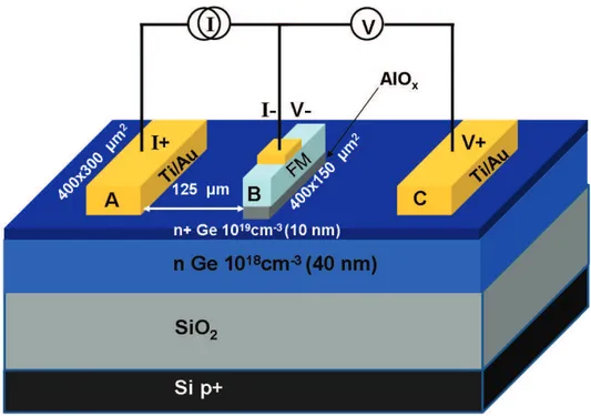
of Fermi level pinning in Ge is pointed out. The rest of the chapter deals with the results obtained for electrical spin injection and detection in n-Ge using FM/oxide contacts. Germanium-on-insulator (GOI) substrates were used to define the Ge channel and three-terminal geometry was used. The results are divided into two parts: first part dealing with Py/Al2O3 devices (low
RA) and second part dealing with CoFeB/MgO devices (high RA). Hanle measurements giving unambiguous proof of spin accumulation in Ge are reported. The effect of surface roughness on spin accumulation is also discussed.
In the fourth chapter, the motivation of using (Ge,Mn) as a spin injector in Ge is presented. The structural and magnetic properties of (Ge,Mn) thin films grown by MBE are discussed. Different (Ge,Mn) nanostructures have been obtained on bulk Ge by changing the growth con-ditions. The magnetic anisotropy in these nanostructures has been investigated using comple-mentary techniques: SQUID and FMR. At the end, the successful growth of (Ge,Mn) layers on Germanium-on-insulator (GOI) substrates is shown and the first step towards using (Ge,Mn) as a spin injector is discussed.
Finally, the conclusion of the thesis and future scope are discussed.
1
Spintronics
The operation of current semiconductor devices is based on the motion of charges. The absence or presence of the charges (electrons or holes) leads to the basic functioning of a device. In past decades, there has been tremendous increase in functionality and performance-to-cost ratio of semiconductor devices by downscaling of device dimensions. This trend is referred to as Moore’s law and it projects that the number of transistors per unit area will approximately double every 18 months [1]. However in near future, simple reduction of length scale cannot continue indefinitely since existing device architectures as well as the material properties will reach their fundamental limitations. In this situation spintronics offers an opportunity to develop new class of materials which could have significant impact on the future of electronics as we move into the 21st century.
Spintronics is a field based on the manipulation of spin degrees of freedom [2]. It uses the spin angular momentum as the basic functional unit rather than charge. An electron can rotate either clockwise or anticlockwise around its own axis with constant frequency, representing two spin states of spin-up (+1/2) and spin-down (-1/2) respectively. The two possible spin states represent the ‘0’ and ’1’ states in logical operations. A two spin channel model was proposed by Mott in 1930s, stating that spin-up and spin-down conduction electrons are two independent families of charge carriers each with its own distinct transport properties [3,4]. This two-current conduction was then confirmed, quantified and modeled around 1970 [5–7].
The first experiments on spin-dependent electron transport phenomena has been performed by Tedrow and Messervey et al. in the early 70s by studying the magnetoresistance of a ferro-magnet/insulator/superconductor (F/I/S) junction [8]. Julliere [9] extended this work to F/I/F junctions leading to discovery of tunneling magnetoresistance (TMR) in this magnetic tunnel junction (MTJ) (Fig.1.1). In MTJ the insulating layer is thin enough (typically a few nanome-ters) for electrons to tunnel from one ferromagnet into the other. TMR is a magnetoresistive effect where the resistance of the junction is lower when the moments of the ferromagnetic layers are parallel. Since tunneling is forbidden in classical physics, the TMR is a strictly quantum mechanical phenomenon. With the advancements of nano-fabricating technologies, Magnetic Random Access Memory (MRAM) and reprogrammable magnetic logic devices have been real-ized based on this effect.
Another great advancement in spintronics was the discovery of giant magnetoresistance (GMR) effect observed independently by the group of Albert Fert [10] and of Peter Gr¨unberg [11]. The GMR is observed in stacks of metallic materials, alternatively magnetic and non-magnetic, as illustrated in Fig. 1.2. There is significant change in the electrical resistance depending on whether the magnetization of adjacent ferromagnetic layers are in a parallel or an antiparallel alignment. The overall resistance can be tuned depending on the relative orientations of the magnetic layers. The first GMR experiments were performed in the current in plane (CIP) ge-ometry. After 1991, experiments in the current perpendicular to the plane of the layers (CPP)
1.1. Spintronics in Semiconductors
Figure 1.1 : A standard magnetic tunnel junction (MTJ) and illustration of Julliere’s model of TMR in MTJ.
geometry have also been performed and have led to the analysis of the physics of spin accumu-lation. The GMR has important applications, in particular for the read heads of hard disks. A hard disk storing binary information can use the difference in resistance between parallel and antiparallel layer alignments as a method of storing 1s and 0s.
The extension of the spintronics in semiconductors promises many new avenues and oppor-tunities that are simply inaccessible in metallic structures. These concepts are discussed in the section below.
1.1
Spintronics in Semiconductors
For extending the applications of spintronics to microelectronics, researchers are interested in the integration of magnetic materials and semiconductors. This is due to the ability to readily control carrier concentrations and transport characteristics in semiconductors via doping and gate voltages. In 1990s experimental studies in GaAs demonstrated spin diffusion lengths of many microns [12,13], spin lifetimes of > 100 ns [14,15] and coherent transport of spin polarized electrons over distances larger than conventional channel lengths. These parameters were many orders of magnitude larger in semiconductors than in metals. This generated excitement for utilizing semiconductors as hosts for spin.
Reduced power consumption is also a major attraction for a spintronic device where the electron spin would transfer and process the information without moving the electron charge. This would lower the power dissipated which is a major issue of conventional electronic semicon-ductor industry. Thus, it would lead to higher speeds and enhanced functionality of the device. Quantum Computing is another possible application of spintronics. There is an advantage of using (electron or nuclear) spins as quantum bits as they can deliver significant speed-up over classical computers.
A semiconductor-based spintronics technology has at least four essential requirements for implementation [16]:
efficient electrical injection of spin-polarized carriers from an appropriate contact into the 12
Figure 1.2 : Schematic picture of the GMR mechanism. device heterostructure,
understanding spin relaxation and knowledge of spin lifetimes,
effective control and manipulation of the spin system to implement the desired function, and
efficient detection of the spin system to determine the output.
1.1.1 Spin Injection and Detection in Semiconductors
In a ferromagnetic metal (FM), the current is spin polarized whereas in non-magnetic material (NM) this is not the case. Spin injection refers to creation of a non-equilibrium spin population in this non-magnetic material. This may be achieved by applying potential difference across FM/NM interface causing spin-polarized electrons from the FM to diffuse into the NM and create a net spin-polarized electron population. Based on this concept Datta and Das [17] in 1990 proposed a first spintronic device concept, a spin transistor, as shown in Fig.1.3. It consists of two ferromagnetic contacts (FM1 and FM2) on both sides of a 2-dimensional electron gas (2DEG). This 2DEG is formed by a heterojunction between two narrow gap semiconductor materials, here InxAl1−xAs and InxGa1−xAs. The FM1 source acts as a spin polarizer and FM2
1.1. Spintronics in Semiconductors as a spin analyzer. There is injection of spin current from FM1 contact into the 2DEG. The length of the channel L, given by the distance between the FM contacts, is less than the spin flip length (lsf) in 2DEG. The spin polarized electrons can enter the analyzer if they both have
same spin orientation. By applying gate voltage, perpendicular to the two dimensional electron gas plane, an effective magnetic field is generated by Rashba spin-orbit interaction (for details see section 1.1.3). This effective magnetic field causes the electron spins to precess and the spin direction is no longer parallel to the source and drain magnetizations direction, hence reducing the flow of spin current. This modulation of electric current by the degree of precession of the electron spin can be introduced by the gate field. The researchers perceive this spin field effect transistor to have technological impact for a variety of new applications in digital semiconductor technology.
Figure 1.3 : Schematic diagram of SFET proposed by Datta and Das [17].
Hammar et. al. made the first attempt to inject spin current in InAs semiconductor having 2DEG using NiFe electrodes [18]. An ohmic contact was formed between NiFe and InAs due to high density of surface states. By changing the relative magnetizations of two electrodes, 0.8% change in resistance was observed. However interpretation of these results was complicated due to the large spurious effects of electrodes eg. anisotropic magnetoresisntace and local hall effects. These results are debatable and were rejected by Van Wees [19] and Monzon et al. [20].
In order to avoid the spurious effects of electrodes and local Hall effect, a non-local geometry was proposed (Fig.1.4(b)). In this geometry, the current path and the detected voltage path are separated. When current flows from ferromagnetic contact (FM1) into a non-magnetic (NM) material (to contact 1), the spin-up electrons are injected into NM, so that the population of spin-up electrons increase by shifting the electrochemical potential (ECP) by ∆µ/2, while those of spin-down electrons decrease by shifting the ECP by ∆µ/2. The total splitting in ECP becomes ∆µ which corresponds to spin accumulation in NM (Fig. 1.4(a)). This spin accumulation diffuses over characteristic length lN Msf , the spin diffusion length in non-magnetic material [21]. The second ferromagnet electrode (FM2) is placed such that it is lying within the lN M
sf from FM1. When the magnetization of FM2 is parallel to FM1, the ECP of spin-up of
FM2 is probed by ECP of spin-up of NM and when they are antiparallel, the spin-down ECP is probed. Therefore, the output voltage (∆VN L) depends on whether the magnetization of FM2
is parallel or antiparallel to that of FM1. Contact 2 is placed beyond the spin diffusion length lN Msf in the non-magnetic material.
Figure 1.4 : (a) Spatial variation of electrochemical potential (ECP) for spin up and spin down electrons at FM/NM interface. (b) Non-local geometry for the spin valve struc-ture. FM1 and FM2 are two ferromagnetic electrodes and NM is the non-magnetic channel. The spin current passing from FM1 to contact 1 creates splitting of the spin-dependent electrochemical potential near the interface. This spin accumula-tion diffuses to FM2 if its placed below spin diffusion length of the NM and creates a voltage difference between FM2 and contact 2. By applying transverse magnetic field spin-polarized carriers precess and dephase in the transport channel.
The spin transport in the non-magnetic channel can be confirmed by observing Hanle effect [22] (see section 1.1.3 for details). A small magnetic field perpendicular to the electron spin direction is applied which causes the spin-polarized carriers to precess and dephase in the trans-port channel. During the time the electrons will travel to FM2, their spins have certain angle. Since ∆VN L is sensitive to the projection of the spins along the FM2 magnetization, it changes
as a function of the field. Hence in non-local geometry electrical injection of spin, accumulation of non-equilibrium spin and electrical detection can be observed. Successful attempts have been done in metallic systems using this non-local geometry with demonstration of Hanle effect [23]. However in the case of semiconductors having ohmic contacts with ferromagnetic electrodes, successful spin injection and detection have been difficult. Several attempts were made in non-local geometry with ohmic contacts between ferromagnetic electrodes like Ni,Co and NiFe on InAs semiconductor having 2DEG but no spin injection was observed [24].
It was finally theoretically demonstrated by Schmidt et al. [25] that negligible spin signal is expected for an ohmic contact between a high-conductivity metallic ferromagnet and a low-conductivity non-magnetic semiconductor. The fundamental reason for the suppression in the spin polarization is the conductivity mismatch. As shown in Fig. 1.5, the current of electrons is spin polarized on the left in FM and non-polarized far on the right in the semiconductor SC. In between, there must be a transfer of current between one of the spin channel to the other one. As discussed before, there is spin accumulation at the interface. The progressive depolarization of the current is related to the spin flips generated by this spin accumulation. The intermediate level of polarization at the interface is simply related to the proportion of the spin flips on the F and N sides. In case of FM/SC interface, the density-of-states is much higher on the FM side and similar spin-accumulation splittings on both sides correspond to a much higher spin accumulation density in FM. For similar spin relaxation times in FM and SC, this leads to a much higher number of spin flips in FM, so that the depolarization of the electron current occurs in FM before the interface. The same depolarization also occurs if DOS are similar, but the spin lifetime is much shorter in the FM.
1.1. Spintronics in Semiconductors
Figure 1.5 : (a) Variation of current spin polarization at FM/SC interface where spin flips on FM side are predominant. (b) Schematic representation of FM/SC contact with and without tunnel barrier. Image taken from ref. [26].
Rashba and Fert proposed that in order to have efficient spin injection from a ferromagnetic metal FM to a semiconductor SC, a spin dependent interface resistance like a tunnel barrier at the FM/SC interfaces can be introduced to promote transfer of one spin type [27,28]. Also by introducing this tunnel barrier, it will not be energetically favorable for spins to flip back in FM leading to increase in spin accumulation in semiconductor (Fig. 1.5(b)). This is discussed in more detail in section below.
Solution to conductivity mismatch- Introduction of a tunnel barrier
In this section, the spin polarization of current at the metal-semiconductor (FM/NM) interface is calculated and how it changes with introduction of a tunnel barrier. These calculations are taken from ref. 28.
Here it is assumed that FM/NM interface is parallel to the xy plane and a current density J parallel to the z axis. For z<0 there is a ferromagnetic metal. In this ferromagnet, the spin-up and spin-down electrons have different conductivities and their resistivities can be given by: ρF M↑(↓) = 2[1 − (+)β]ρF. Here β is dimensionless bulk asymmetry parameter given by β =
ρF M ↑ −ρF M↓
ρF M ↑ +ρ
F M
↓ , here the spin direction of the electrons ↑ (↓) refers to the majority (minority) spin
direction in a ferromagnetic material and ρF M↑ , ρF M↓ are the resistivities for the spins ↑ and ↓ respectively. For z>0, there is a semiconductor with equal conductivities of spin-up and spin-down electrons. Their resistivity is given by ρN M
↑ = ρN M↓ = 2ρN M.
Here assuming that the spin-scattering occurs on a much slower timescale than other electron scattering events, there exists two electrochemical potentials (µ+, µ−) which need not be equal.
+(−) refers to the absolute spin direction of the electrons. If the current flow is one dimensional, 16
e.g. in the z direction, the electrochemical potentials are connected to the current via the resistivity, the diffusion constant D and the spin-flip time constant τsf by the following
drift-diffusion equations: j = j++ j− (1.1) ∂µ+,− ∂z = −eρ+,−j+,− (1.2) µ+− µ− τsf = D∂ 2(µ +− µ−) ∂x2 (1.3)
These equations can be solved by following boundary conditions:
∆µ(z = −∞) = ∆µ(z = +∞) = 0 (1.4)
At z=0, there exists continuity in j+ and j−:
∆j(z = 0−) = ∆j(z = 0+) (1.5)
There is also continuity in electrochemical potentials (µ+ and µ−), however there is
discon-tinuity with existence of an interface resistance:
µN M+(−)(z = 0+) − µF M+(−)(z = 0−) = er+(−)j+(−)(z = 0) (1.6)
where r+(−) = 2r∗
b[1 − (+)γ] and rb∗ is the resistance of interface layer and γ is its spin
asymmetry coefficient. In absence of an interface resistance r↑(↓) becomes zero.
The solution of the above equations can be written as:
µF M+(−)= eρ∗F M(1 − β2)Jz− (+)B[1 − (+)β]exp( z lF Msf ) + C (1.7) J+(−)F M = [1 + (−)β]J 2 − (+) B 2erF M exp( z lF M sf ) (1.8) µN M+(−)= eρNJz− (+)Dexp(− z lN M sf ) (1.9) J+(−)N M = J 2 + (−) D 2erNexp(− z lN Msf ) (1.10) Hence we get, ∆µF M = Eexp(z/lsfF M) (1.11) ∆µN M = F exp(−z/lN Msf ) (1.12)
here B, C, D, E and F are constants and can be calculated using boundary conditions. So in absence of interface, the spin accumulation (µ+− µ−) has the same value on both sides of
the interface and when one goes away from the interface it decreases exponentially with decay lengths lF Msf on FM side and lN Msf on NM side (Fig.1.6(a)). The polarization of current injected into the semiconductor is given by:
1.1. Spintronics in Semiconductors (SP )N M(z) = j N M + (z) − j−N M(z) jN M + (z) + j−N M(z) (1.13) = βrF M + γr ∗ b rF M + rN M+ rb∗ (1.14) here rF M and rN M are given by the products of the resistivity by the spin diffusion length
for the ferromagnetic and nonmagnetic materials, respectively: rF M = ρ∗F M × lF Msf and rN M =
ρ∗
N M× lsfN M. If we consider the case when both FM and NM are metals, without any interface
layer, then the equation can be written as:
SP = β
1 + rN M/rF M
(1.15)
Figure 1.6 : (a) Variation of the electrochemical potentials (µ+ and µ−) as a function of z
at a Co/Cu interface without interface resistance. The inset shows the variation of the spin accumulation parameter, ∆µ = (µ+− µ−). (b) Spin polarization of
the current as a function of z at the FM/NM interface. Curve 1 is for Co and Cu without interface resistance. Curve 2 is for Co and a semiconductor without interface resistance. Curve 3 is for Co and a semiconductor with a spin dependent resistance (tunnel junction) at the interface. The spin polarization is γ/2 at the interface for the particular case r∗b = rN M >> rF M of curve 3.
Taking example of Co and Cu (rCu = 6 × 10⁻¹⁵Ωm2 and (rCo= 4.5 × 10⁻¹⁵Ωm2), the
spin-polarization penetrating the NM becomes SP=β/2.33, indicating that the current penetrating the non-magnetic metal is only moderately reduced from its value β inside the ferromagnet.
Now if we consider only a FM and a semiconductor, we have six orders of magnitude of difference in the resistance, hence leading to a strong reduction of the spin polarization. Also from calculations it is found that the current spin polarization on either side is proportional to the total numbers of spin flips and these spin flips are proportional to 1/rF M and 1/rN M in FM
and NM respectively. With rF M << rN M, this means that there are much more spin-flips and a
stronger depolarization of the current in FM than in NM. In other words, the current is already completely depolarized when it crosses the interface (Fig. 1.6b).
Inserting a high interface resistance with rb∗> rN M leads to high spin polarization. For rb∗=
rN M >> rF M, this spin-polarization is given by γ/2. In the limiting case for rb∗ >> rN M > rF M,
the spin polarization at the interface is simply the spin asymmetry coefficient of the interface resistance:
SP = γ (1.16) The high interface resistance and the high asymmetry coefficient γ can be obtained by introducing ultra-thin insulating layers i.e. tunnel barriers of Al2O3 or MgO at the interface.
This tunnel barrier brings discontinuity in the ∆µ, being much higher in NM. This leads to a more balanced number of spin flips in FM and NM, and hence restores the spin polarization at the interface and in the semiconductor.
Tailored Schottky tunnel barriers
Tailored Schottky barriers can act as effective tunnel barriers by heavily doping the semicon-ductor surface layer. In a normal Schottky barrier between a semiconsemicon-ductor and a FM, e.g. in the case of GaAs with doping of ND ≈ 1017 cm−3 and a FM (like Fe, Co, Ni) there is a barrier
height of 0.5 − 0.8 eV and a depletion width of 90 nm (Fig. 1.7(a)). This large barrier height and high depletion width leads to negligible spin injection in reverse bias condition from FM to semiconductor. However when the depletion region of the Schottky diode is sufficiently nar-row, tunneling between the ferromagnetic metal and the semiconductor becomes the dominant transport process. The surface layers of semiconductor can be highly doped by introducing a n++ layer between FM and n-GaAs, reducing the depletion width to around 10-15 nm which acts as a tunnel barrier for spin injection. This is also known as tailored Schottky contact. The tunnel barrier hence formed circumvents the constraint of mismatched conductivity between the contact and semiconductor.
Figure 1.7 : (a) Band diagram of Schottky barriers for Fe/GaAs junctions of different dop-ing densities. As the dopdop-ing density increases, the depletion layer width becomes thinner and the Fermi level merges with the conduction band. The electrons can tunnel through the think Schottky barrier. (b) Spin-LED structure used by Zhu et al. [29] consisting of an Fe Schottky contact to a GaAs/InGaAs Quantum well LED detector.
The first evidence of spin injection in GaAs semiconductor from ferromagnetic Fe contact was shown in 2001 by Zhu et al. [29]. They used an Fe film epitaxially grown onto a GaAs/GaInAs LED structure (Fig. 1.7(b)). The spin injection efficiency was investigated by analyzing the
1.1. Spintronics in Semiconductors degree of circular polarization of light emitted by the LED. They observed spin injection with circular polarization degrees of about 2% up to room-temperature.
Eventually, in 2003 Hanbicki et al. [30, 31] tailored the Schottky barrier between Fe and AlGaAs by heavily doping the surface layers of semiconductor, steeply increasing the doping level from 1016cm−3 to 1019cm−3. The detailed analysis of the transport process over the Fe/GaAs interface showed a single-step tunneling mechanism as dominant conduction mechanism. They used spin-LED structure having a GaAs quantum well and measured the circular polarization of the emitted light. They reported a spin injection polarization of about 30% at room-temperature. In 2005, Crooker et al. [32] directly imaged electrical spin injection and accumulation in the GaAs channel of lateral spin-transport device having Fe/GaAs tailored Schottky contacts (Fig. 1.8(a)). Scanning Kerr microscopy was used to image the spin transport in the 300 mm long channel region. Images of the steady-state perpendicular component of spin polarization in the n-GaAs channel near the source and drain contacts (Fig. 1.8(b)) show injection and lateral flow of spin-polarized electrons. The perpendicular component is studied because Kerr effect is much higher in polar geometry and this component is present due to precession of spins in perpendicular magnetic field. The injected spins are accumulated near the injector contact and decay with distance due to spin relaxation in GaAs. Also there is spin accumulation at detector contact due to selective extraction of electron spins.
Figure 1.8 : (a) Photo-micrograph of the spin injection device. Spin polarized electrons are injected from Fe into GaAs. (b) Image of the perpendicular component of spin accumulation in a GaAs channel by a scanning Kerr microscope.
Lou et al. in 2006, demonstrated electrical spin injection and detection in Fe/GaAs tailored Schottky contact [33]. The geometry of their device is shown in Fig. 1.9. The n-GaAs channel had a doping level of 3.6 × 1016cm−3 with a surface layer with doping level of 5 × 1018cm−3.
They observed accumulation of spin polarized electrons in forward-biased Fe/GaAs contact. Their results were in agreement with the model of Ciuti et al.[34], where the effective resistance of the Schottky barrier is higher when a spin accumulation in the semiconductor is present. The barrier is less transmissive for the spin state that accumulates in the semiconductor. Moreover, the Hanle effect, modulation of spin current by applying transverse magnetic field, was also shown. The spin signal was observed up to 60 K.
Figure 1.9 : Photomicrograph of the Fe/GaAs device used by Lou [33]. Hanle-effect observed at different temperatures is also shown.
In 2007, Lou et al. demonstrated the first successful electrical detection of spin injection using a non-local geometry in Fe/GaAs contact at 50K [35]. The schematic diagram of their device is shown in Fig.1.10. Spin-polarized electrons are injected from Fe into the GaAs channel through a tunneling Schottky barrier at contact 3 towards contact 1. This causes spin accumulation in GaAs as the population of spin up and spin down electrons becomes unequal. Although electrons flow from 3 to 1, the non-equilibrium spin polarization in GaAs, represented by purple arrows can diffuse in either direction from the source. The non-local voltage is thus measured between contacts 4 and 5. A change of 16.8µV in non-local voltage (V4−5) was observed for
parallel and anti-parallel orientations of the two contacts. They also observed the Hanle effect. The difference in two Hanle signal for different orientation of electrodes was found to be 18µ V. This voltage difference is given as:
V↑↓− V↑↑=
2γβF e(SP )GaAsEf
3e (1.17)
here γ is the spin transmission efficiency of the interface ≈ 0.5, e the electronic charge, βF e
the spin polarization in Fe ≈ 0.42, Ef the Fermi energy and (SP )GaAs the spin polarization in
GaAs to be calculated. At distance of 12µm from the source, the value of SPGaAs was found
to be 0.02, hence successfully demonstrating the electrical spin injection and detection using Schottky-tunnel barrier contacts.
However in case of spin injection from Schottky barrier, the quality of interface plays a very important role. Since the ferromagnetic metal and semiconductor are in direct contact, any structural disorder at the interface will drastically reduce the spin polarization. A good chemical stability of the interface is the prerequisite for high efficiency of device. The growth temperature of metal on semiconductor is of crucial importance because magnetic atoms can diffuse into the semiconductor. These magnetic atoms carrying a local magnetic moment scatter the spin in semiconductor channel and hence degrades the spin polarization. The second disadvantage of Schottky barrier for spin injection is that tunneling is not possible on both ends of the device. When the spin injection is carried by reverse biasing the injector FM-SC Schottky contact, the detector end will be automatically forward biased. This would remove the Schottky tunnel
1.1. Spintronics in Semiconductors
Figure 1.10 : (a) A schematic diagram of the non-local experiment used in ref. 35. The five Fe contacts having in-plane easy axes on GaAs channel. The large arrows indicate the magnetizations of the source and detector. Electrons are injected along the path shown in red. The injected spins (purple) diffuse in either direction from contact 3. The non-local voltage is detected at contact 4. (b) Non-local voltage, V4−5, versus in-plane magnetic field at a current I1−3= 1 mA at T=50 K. (c)
Non-local voltage, V4−5, versus perpendicular magnetic field, Bz, for the same
contacts and bias conditions.
barrier and both spin-up and spin-down electrons can enter into the detector without spin filtering. This reduces the spin detection efficiency. Both the above problems can be solved by using a insulating tunnel barrier between FM and a semiconductor for efficient spin injection. Oxide tunnel barrier
The insertion of insulating tunnel barrier like Al2O3, MgO or SiO2between a FM/semiconductor
interface can be employed for efficient spin injection. It introduces a spin-dependent drop of the electrochemical potentials at the interface with discontinuous ∆µ at the interface and an enhancement of the spin accumulation in semiconductor. It also provides chemical stability at the interface and tunnel barriers are formed at both ends of device (injector and detector).
The maximum tunneling spin polarization which can be obtained in case of FM/Al2O3 is
50%. This is due to the amporphous nature of the layer which causes spin scattering and depolarization of spin [36,37]. However for crystalline MgO, the tunneling spin polarization of FM/MgO is predicted to be very high due to coherent tunneling of spin polarized electrons [38]. It has been found that in a structure like Fe/MgO(001)/Fe, the tunneling magnetoresistance ratio is in excess of 1000% for an MgO (100) barrier of ≈ 20 atomic planes.
In a device with lateral geometry, it was theoretically explained by Fert et al. that high values of magnetoresistance (MR) for FM/I/NM/I/FM structure can be observed only if the
Figure 1.11 : (a) ∆R/Rp for the lateral geometry given in (b) as a function of rb∗/rN M for
different values of tN M/lN Msf . The calculations were performed for rF M = 4.5 ×
10−15Ωm2 << rN M = 4 × 10⁻⁹Ωm2, β = 0.46, γ = 0.5. (b) Lateral geometry
with the same widths W for the FM and NM channels. (c) Lateral geometry with different widths W and w for FM and NM channels. Also the NM channel extends to infinity at both ends. Images taken from ref. 28
resistance-area (RA) product of both the FM/I/NM contacts lie in a narrow range [28]. The tunnel barrier resistance r∗
b (the RA product of the tunnel contact) should lie in this optimum
range:
rN MtN M/lN Msf < rb∗< rN MlsfN M/tN M (1.18)
This condition is true only for tN M << lsfN M and the value of MR obtained as a function of
r∗b for different values of tN M/lsfN M is shown in Fig. 1.11(a). This is for lateral geometry shown
in Fig. 1.11(b). The lower edge condition rN MtN M/lsfN M < r∗b is required so that the resistance
of the tunnel contact is larger than a critical value to overcome the conductivity mismatch. If r∗b << rN MtN M/lN Msf , then the discontinuities in the electrochemical potentials (µ↑ and µ↓)
introduced by the interface resistances are too small to generate a high enough splitting ∆µN M
and polarize the current in semiconductor. The condition corresponding to the upper edge of the window, rb∗ < rN MlsfN M/tN M, is the condition for spin conservation, or more precisely,
optimal conservation of the spin accumulation occurring in the anti-parallel configuration. If r∗b >> rN MlsfN M/tN M, the spin accumulation ∆µN M of the AP configuration is completely
relaxed by the spin flips in the volume tN M of the semiconductor leading to negligible MR.
In the structure of Fig.1.11(c), where FM and NM channels have different widths (W and w) and also the NM layer spreads from −∞ to +∞ towards the left and the right in the horizontal plane, the spin accumulation ∆µ spreads over lN M
sf on both sides of tN M. Consequently, the
relaxation in NM is enhanced by the factor (W/w)(lN M
sf /tN M) and the condition for large MR
becomes rN M(tN M/lN Msf )2(W/w) < r∗b < rN M(W/w) [28]. The correction factor W/w applies
only when the lateral dimensions of the contact are smaller than the spin-diffusion length. For electrical injection and optical detection of spin polarization the lower edge condition should be satisfied. However for both electrical injection and detection both conditions should be satisfied. The tailoring of the RA product of the tunnel contact to satisfy these conditions can be done by either by heavily doping the semiconductor surface layer (to reduce the depletion
1.1. Spintronics in Semiconductors zone) or by changing the resistance of tunnel barrier.
The electrical spin injection in semiconductor using Al2O3 tunnel barrier was demonstrated
in GaAs LED system in vertical geometry by Motsnyi et al. [37]. The detection was done optically by oblique Hanle-effect and measuring the circular polarization of the emitted light. They found spin injection efficiency of more than 9% at 80 K. By replacing the Alumina barrier by crystalline MgO by Jiang et al., the efficiency was improved to 50% [39]. Similarly in Si, successful injection of spin-polarized electrons through an Al2O3 tunnel barrier was shown by
Jonker et al. [40]. The spins were electrically injected from a thin ferromagnetic Fe film through an Al2O3 tunnel barrier into a Si(001) n-i-p doped heterostructure, and the detection was done
optically. A spin polarization of 3% was measured optically and by using correction factor a value of 30% was obtained at 5 K.
The first results of electrical spin injection and detection in Si were published by Appelbaum et al. in 2007 [41]. They showed the injection of high energy hot electrons from a source of Aluminium and polarized by CoFe electrode at 85 K (Fig.1.12). After vertical transport through undoped Si, the spin polarization of the conduction-band electrons was detected electrically by another ferromagnetic NiFe electrode. The proof of spin transport in Si was seen by change in collector current by changing the relative magnetizations of two ferromagnetic electrodes. Also dephasing spin by applying weak transverse magnetic field, precession angles of up to 4π were observed.
Figure 1.12 : Schematic band diagram of the device used by Appelbaum [41] for transport of hot electrons in Silicon. Precession angles up to 4π were observed by applying perpendicular magnetic field at 85 K.
In the same year, van’t Erve et al. demonstrated electrical spin injection and detection in n-Si at 5K using Fe/Al2O3 tunnel barrier contacts in non-local lateral geometry (1.13(a))[42]. They
observed change in non-local voltage with change in relative magnetizations of the electrodes. The confirmation of spin transport and a demonstration of spin modulation in the silicon was provided by the Hanle effect. Eventually the first results of spin injection in Silicon at room temperature were published by Dash et al. [43]. They used a three-terminal geometry in which injection and detection is done under the same electrode ( 1.13(b)). They demonstrated electrical injection of spin polarization into n-type and p-type silicon from a ferromagnetic tunnel contact, spin manipulation using the Hanle effect and the electrical detection of the induced spin accumulation. A spin splitting of 2.9 meV was observed in n-type silicon, corresponding to an estimated electron spin polarization of 4.6%. The spin lifetime greater than 140 ps was extracted for conduction electrons in heavily doped n-type silicon at 300 K and greater than 270 ps for holes in heavily doped p-type silicon at the same temperature. The spin diffusion length greater than 230 nm for electrons and 310 nm for holes in the corresponding materials was found.
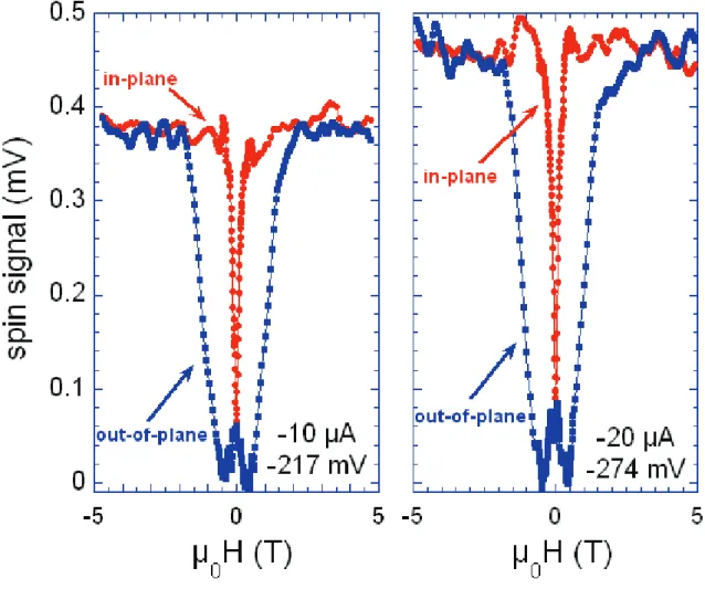
(The low values of spin lifetime was found due to artificial brodening of the Hanle curves. The surface roughness at the interface leads to magnetostatic charges which produces local fields and drastically affect spin accumulation [44]. This phenomenon is discussed in detail in chapter 3). Since then, the experimental progress for spin transport in semiconductors has been fascinating by utlilizing oxide tunnel barrier and various works have been published.
Figure 1.13 : (a) Non-local geometry used by van’t Erve et al. [42] for spin injection in Si using Fe/Al2O3 spin injector. The non-local voltage measured as a function of
in-plane and out-of-in-plane magnetic field at 10 K is also shown. (b) Three terminal geometry employed by Dash et al. [43] where injection and detection is done under same contact. Change in detected voltage as a function of perpendicular field is also shown at different temperatures.
Thus, using a insulating tunnel barrier between FM and semiconductor interface solves the problem of conductivity mismatch and leads to efficient spin injection. This barrier should be free of any pin-holes and thermally stable for the device to function properly at higher temperatures. The crystalline MgO barrier provides more tunneling spin polarization than amorphous Al2O3
barrier. Finally the RA product of the barrier should lie in an optimum range to have the highest values of magnetoresistance.
Ferromagnetic Semiconductors
One more solution to have spin injection in semiconductors is to use magnetic semiconductors as spin injectors instead of metals. The magnetic semiconductors exhibit both ferromagnetism and semiconductor properties and hence match the resistance of the semiconductors. The magnetic semiconductors can be divided into three categories depending on the distribution of magnetic atoms:
Concentrated Magnetic Semiconductors
Concentrated magnetic semiconductors (CMS) are alloys of magnetic atoms with semi-conducting materials. Here the magnetic atoms sit in well defined lattice sites in the crystalline structure. Some examples are europium chalcogenides (Eus, EuSe) and semi-conducting spinels like CdCr2Se4 or CuCr2S4 (the proportion of magnetic atoms being
1.1. Spintronics in Semiconductors 28.6%). However these materials have different crystal structure than that of Si, GaAs limiting their integration in existing semiconductor industry.
Dilute Magnetic Semiconductors (DMS)
The non-magnetic semiconductors are doped with small amount of magnetic atoms (few percent) to make them magnetic, called as Diluted Magnetic Semiconductors. The mag-netic atoms substitute the atoms of semiconductor matrix without changing significantly the crystalline structure. In beginning the research was focused on II-VI-based compound semiconductors such as CdTe or ZnSe, doping them with magnetic 3d transition metals. However, their Curie temperatures was quite low.
Figure 1.14 : Three types of semiconductors: (A) a magnetic semiconductor, in which a periodic array of magnetic element is present; (B) a diluted magnetic semiconductor, an alloy between nonmagnetic semiconductor and magnetic element; and (C) a nonmagnetic semiconductor, which contains non magnetic ions. (from ref. 45) In the 1990s, III-V based DMS were fabricated by doping with Mn atoms. However the low solubility of Mn in III-V was improved by using non-equilibrium growth techniques like low temperature molecular beam epitaxy. It was also observed that the carrier density plays important role in the mediation of ferromagnetism. In 2000 a model (Zener Model and mean field approximation) was proposed to explain the origin of magnetism in II-VI and III-V DMS and the relation of Tc with the concentration of magnetic atoms and the
carrier density [46].
In III-V DMS Mn atoms replace Ga atoms and provide both magnetic moments and holes due to their valence different from Ga. However in II-VI DMS, Mn atoms have the same valence as the cations and act as localized magnetic moments without changing the carrier density. Thus, additional conventional doping is required to tune the carrier density. Despite those advances, experimental results in II-VI systems have shown rather low Tc
and focus moved on to III-V and IV semiconducting hosts. The theoretical prediction of Curie temperatures Tc by Zener model for different DMSs is shown in Fig. 1.15. Up to
now, Tc up to 190 K have been achieved in (Ga,Mn)As, and major efforts are made to
reach Tc’s above room temperature [47,48].
Non-uniform magnetic semiconductors
Non-uniform magnetic semiconductors, also known as heterogeneous semiconductors, are group of magnetic semiconductors which originates from DMS. During non-equilibrium growth of DMS systems, when the magnetic element concentration far exceeds the sol-ubility limit, there may be formation of unknown, metastable phases. A spinodal de-composition occurs for such systems leading to the formation of such metastable phases
Figure 1.15 : Computed value of the Curie temperature TC by Zener’s model for various p-type
semiconductors containing 5% Mn and 3.5 × 10²⁰ holes at different temperatures [46].
which exhibit higher Tc than the DMS films. These phases are fully coherent with the
surrounding matrix but still show locally higher concentration of magnetic atoms. The first theoretical explanation for this phenomenon was given by Sato et. al. who calculated an increase of Tc upon phase decomposition due the extended magnetic networks in the
system [49]. This spinodal decomposition has been reported in different II-VI, III-V and IV systems, such as, e.g., in (Zn,Cr)Te by Kuroda et al. [50], in (Ga,N)Fe by Bonanni et al. [51], in (Ga,Mn)As by Hai et al. [52], or in (Ge,Mn) by Jamet et al. [53].
The first result of using DMS as a spin aligner (Fig.1.16) was shown in BexMnyZn1−x−ySe
by Fiederling et al. [54]. A large magnetic field parallel to the growth direction was applied and full polarization of carriers in the DMS layer was created by giant Zeeman splitting. The polarized spins entered the AlGaAs channel and 90% spin polarization was observed by electro-luminescence. Jonker et al. also achieved similar results using Zn1−xMnxSe as a spin-injecting
contact on a GaAs-based light-emitting diode [55]. At the same time, Y. Ohno et al. [56] published results showing the injection of spin polarized holes from magnetic GaMnAs into the active region of a spin LED (InGaAs/GaAs quantum well). The circular polarization of the light emitted along the edge of the sample (perpendicular to the growth direction) was measured to be about 1%. However, these results are debated and it is argued that there are different selection rules for edge-emission (side emission) and surface emission using quantum wells [57].
In 2003, Mattana et al. illustrated electrical spin injection and detection in GaAs quantum
well using GaMnAs ferromagnetic electrodes [58]. A vertical structure of GaMnAs/AlAs/GaAs/AlAs/GaMnAs having double tunnel junction and two GaMnAs electrodes with different thicknesses and
dif-1.1. Spintronics in Semiconductors ferent Mn concentrations was used in order to obtain different coercive fields. A TMR ratio of 38% was observed at 4 K.
Figure 1.16 : (a) Schematic band structure of the spin-aligner light-emitting diode. Spin-polarized electrons are injected from the left into the active GaAs layer, unpo-larized holes from the right, (b) Side view of the device showing the direction of the magnetic field and the emitted light. (c) Degree of circular polarization of the electroluminescence observed for different values of dSM and dNM. For more detais see ref. 54.
The electrical spin injection and detection in non-local lateral geometry using GaMnAs DMS was done by Ciorga et al in 2009 [59]. They used p+GaMnAs/n+GaAs ferromagnetic
Esaki diodes [60] as spin aligning contacts for spin injection and detection in n-GaAs channel. This Esaki diode under reverse-bias allows spin-polarized tunneling of electrons from the valence band of (Ga,Mn)As to the conduction band of n+GaAs. They successfully demonstrated the
spin-valve effect, Hanle-effect and extracted the value of 50% for spin-injection efficiency. The results may open new possibilities for spin-current-induced magnetization switching (CIMS) in (Ga,Mn)As and one could realize all-semiconductor spin devices.
1.1.2 Spin Relaxation in Semiconductors
Spin relaxation is the decaying of initial non-equilibrium spin polarization. It can occur due to combination of momentum scattering and spin-orbit interaction or due to precession of spins around a random fluctuating magnetic field or due to emission/absorption of magnetic excita-tions (like magnons in FM). The random magnetic field can be described by two parameters:
its amplitude, referred to by the average spin precession frequency in the random field, ω and its correlation time τc, the time during which the field may be considered as constant.
The spin makes a precession around the (random) direction of the effective magnetic field with a typical frequency ω and during a typical time τc. After a time τc the direction and the
absolute value of the field change randomly, and the spin starts its precession around the new direction of the field. After a certain number of such steps the initial spin direction will be completely lost. The dimensionless parameter ωτc is the typical angle of spin precession during
the correlation time. We can consider two limiting cases for the product ωτc:
ωτc << 1
In this case the electron spin undergoes a very small precession during the correlation time ωτc and the spin undergoes a small angular diffusion. During a time t, the number
of random steps is t/τc, for each step the squared precession angle is (ωτc)2. These steps
are not correlated, so that the total squared angle after a time t is (ωτc)2(t/τc). The spin
relaxation time τs may be defined as the time at which this angle becomes of the order of
1. Hence, 1 τs ≈ ω 2τ c (1.19) ωτc >> 1
This means that during the correlation time the spin will make many rotations around the direction of the magnetic field. Hence the spin will be lost in a time of the order of τc:
τs≈ τc (1.20)
This consideration is quite general and applies to any mechanism of spin relaxation. We only have to estimate the values of the relevant parameters ω and τc for a given mechanism.
In most cases spin-orbit coupling is responsible for spin relaxation. Spin-Orbit Coupling
A particle moving with velocity ~v in an electric field ~E will experience a magnetic field given by ~B = (1/c2) ~E × ~v, where c is the velocity of light. Similarly in a rest frame of electron, the
electric field from charge +Ze in nucleus is seen as a magnetic field. This magnetic field acts on the electron magnetic moment. The radial electric field can be given as ~E = 1e∂U (r)∂r u~r, where
U (r) is potential of the electron. Also the angular momentum ~L can be written asL = ~~~ ur× m~v.
This makes the effective magnetic field as: ~ Bef f = 1 meec2 1 r ∂U (r) ∂r L~ (1.21)
This field is perpendicular both to ~E and ~v is normal to the plane of the orbit, thus it is parallel to the orbital angular momentum L. This is the physical origin of the spin-orbit interaction and this effect is relativistic and quantum mechanical.
The magnetic moment of an electron with spin ~S is given by ~µ = −gµB
~ S where g is the~
Lande factor and µB is Bohr magneton. In a magnetic field this magnetic moment will have
energy, Zeeman energy, H = −~µ. ~B. Thus in the above magnetic field due to spin-orbit coupling, the energy associated can be given as:
H = µB ~meec2 1 r ∂U (r) ∂r L.~~ S (1.22)
1.1. Spintronics in Semiconductors Thus the spin-orbit interaction can be written as A(~L.~S), the constant A depending on the electron state in an atom. This interaction results in a splitting of atomic levels, which strongly increases for heavy atoms. This spin-orbit interaction is responsible for band split-off in valence band which is observed in semiconductors at ~k = ~0 and is given in the table 1.1.
Material Esplit−of f
GaAs 0.34 eV Ge 0.29 eV Si 0.05 eV
Table 1.1 : The band split-off in valence band for different semiconductors.
Different mechanisms for spin relaxation
There are several possible mechanisms responsible for spin relaxation. The Elliott-Yafet (EY) Mechanism
ElliotYafet (EY) spin scattering refers to processes in which an electron scatters from a specific defect within the semiconductor in a manner that causes the electron to flip its spin. These defects may be structural defects such as misfit dislocations, grain boundaries, or local impurities, or they may be dynamic defects such as phonons. The electrical field, accompanying lattice vibrations, or the electric field of charged impurities is transformed to a magnetic field through a spin-orbit coupling [61,62].
Due to this spin-orbital interaction, real crystals Bloch states (i.e momentum eigenstates) are not spin-eigenstates anymore. The magnetic field lifts-off the spin degeneracy of the Bloch states and mixes spin-up and spin-down states. This occurs because the spin com-ponent of wave functions do not factorize into a single product of a purely orbital wave function and a purely spin component. The correlation between the spin component of the wave function and the orbital component of the wave function differs for electronic states with different momenta, and thus non-magnetic scattering from one state with momentum ~k1 to another state with momentum ~k2 will lead to a small probability of a spin flip. This
happens even when the materials are inversion symmetric, and the dispersion relations are doubly degenerate at each momentum k, because it is still not possible to factorize states at a given momentum into an orbital and a spin part.
The spin relaxation rate is proportional to momentum scattering rate and hence it increases with increase in the impurity concentration. For temperature dependence, spin relaxation by impurities occurs at lower temperatures and by phonons at higher temperatures. There-fore a weak temperature dependence of the spin relaxation rate (1/τs) is observed at lower
temperatures but as temperature increases phonon scattering becomes dominant and much higher temperature dependence is observed. This scattering mechanism is dominant for inversion-symmetric materials, such as simple metals and semiconductors like Silicon and Germanium.
The D’yakonov-Perel’ mechanism
This spin relaxation mechanism is related to the spin-orbit splitting of the conduction band of semiconductors that lack inversion symmetry. As the electron moves, the combination of spin-orbit interaction and the inversion asymmetry of the material causes it to feel an effective magnetic field. This field lifts the degeneracy of the momentum states of the spin-up and spin-down electrons: Ek↑6= Ek↓i.e. having the same momentum state but different
energies. Most prominent examples of materials without inversion symmetry come from groups III-V (such as GaAs) and II-VI (ZnSe) semiconductors, where inversion symmetry
is broken by the presence of two distinct atoms in the Bravais lattice. In heterostructures the symmetry is broken by the presence of asymmetric confining potentials.
For bulk semiconductors, this splitting was first pointed out by Dresselhaus [63]. The ad-ditional spin-dependent term in the electron Hamiltonian can be presented as gµ ~B(~k).~S = ~~Ω(~k).~S, which can be viewed as the energy of a spin in an effective magnetic field. Here ~
Ω(~k) is a vector depending on orientation of the electron momentum with respect to the crystal axes. Hence the energy of an electron in the conduction band, should be written in the form:
E(~k) = (~k)
2
2m∗ + ~~Ω(~k).~S (1.23)
For a given ~k, ~Ω(~k) is the spin precession frequency. In an effective field ~Bef f, this
frequency is given by ~Ω(~k) = e~mB~ef f(~k). This effective magnetic field is inhomogeneous in
momentum space. This implies that the effective magnetic field changes in time because the direction of ~k varies due to electron collisions. Thus the correlation time τc is on the
same order of the momentum relaxation time τk and if Ωτk is small, the spin relaxation
rate from eqn. 1.19 is given by:
1 τs ≈ Ω
2τ
k (1.24)
Figure 1.17 : (a) Evolution of a single carrier in the presence of the effective magnetic field B(k) and orbital scattering. Both the spin orientation and the momentum of the carrier is altered. (b) Evolution of a population of carriers under the same conditions. Different precession rates and orientations of carriers with different momenta lead to different spin directions for different carriers. Orbital deco-herence averages spin orientation, yielding a spin polarization reduced from the initial value.
In contrast to the Elliott-Yafet mechanism, now the spin relaxation rate is inversely propor-tional to momentum scattering rate. The spin rotates not during but between the collisions
1.1. Spintronics in Semiconductors and therefore the relaxation rate increases when the impurity concentration decreases. For an electron gas in equilibrium, the average magnetic field vanishes, but the variance of the magnetic field does not. As carriers scatter from momentum state to momentum state, they feel a time-dependent effective fluctuating field.
This spin relaxation mechanism is predominant at higher temperatures (> 70K). Elemental semiconductors like Si, Ge possess inversion symmetry in the bulk, so the D’yakonov-Perel’ mechanism does not apply to them. Hence the spin lifetime in these systems can exceed the spin lifetimes in III-V semiconductors by orders of magnitude [64].
The Bir-Aronov-Pikus mechanism
This is a mechanism of spin relaxation of non-equilibrium electrons in p-type semiconduc-tors due to the exchange interaction between the electron and hole spins. This was first observed by Bir et al. in 1975 [65]. The exchange interaction between electrons and holes is governed by the Hamiltonian:
H = A~S. ~Jδ(~r) (1.25)
where A is proportional to the exchange integral between the conduction and valence states, ~J is the angular momentum operator for holes, ~S is the electron-spin operator, and ~r is the relative position of electrons and holes. The spin-flip scattering probability depends on the state of the holes (degenerate or non-degenerate, bound on acceptors or free). Holes have shorter spin coherence times, and spin exchange between electrons and holes is very effective. Ultimately, it will lead to spin decoherence of electrons. This spin relaxation rate, being proportional to the number of holes, may become the dominant one in heavily p-doped semiconductors. This mechanism is of importance at low temperatures [66].
Hyperfine-interactions
Hyperfine-interaction comes from the magnetic interaction between the magnetic momen-tum of nuclei and electrons. The electron spin interacts with the spins of the lattice nuclei which provide a random effective magnetic field. In most III-V semiconductors, all the nuclei have non-zero spin, and can engage in mutual spinflip processes with electrons and holes in a process analogous to the BAP process described above. A key difference is the short-range, weak coupling that characterizes the hyperfine interaction. The hyperfine in-teraction is only significant for electrons in localized states such as quantum dots or dilute dopant levels.
1.1.3 Manipulation of spin polarization
For realization of spin-transistor as proposed by Datta and Das, its necessary to manipulate the spins in the channel of the transistor. This can be mostly done in two ways: either by applying external magnetic field or utilizing Rashba effect by applying electric field. However, recently it was shown that temperature gradient (Spin Seebeck effect [67]) and optical methods [68] can be used to manipulate spin, but these are not discussed here.
Manipulation of spins by external magnetic field
Upon the application of a magnetic field ~B the electron spins, or rather the spin magnetization ~
m experiences a torque. This torque ~Γ is given by:
~Γ = ~m × ~B (1.26)
Under this torque, the spins will precess around the field at a frequency, known as Larmor frequency given by Ω = ge 2mB (1.27)
The precessional motion is altered by damping caused by spin relaxation and the creation or recombination of electrons. This precession, along with spin creation, spin relaxation, and recombination is described by the following simple equation of motion of the average spin vector
~ S: d~S dt = ~ So− ~S τ − ~ S τs + ~Ω × ~S (1.28)
Here the first term on right-side denotes the spin generation (So/τ ) and recombination (S/τ )
with electron lifetime τ , the second term describes spin relaxation with spin relaxation time τs
and third term denotes the spin precession in magnetic field with frequency Ω. The spin lifetime is defined as (τsf−1 = τ−1+ τ−1
s ).
In the stationary state (dS/dt = 0) and in the absence of a magnetic field, one finds: Sz(0) =
So
1 + τ /τs
(1.29) where Sz(0) is projection of the spin on the direction of So (z -axis). In the presence of
magnetic field we obtain:
Sz(B) =
Sz(0)
1 + (Ωτsf)2
(1.30) Hence in static conditions, the spin projection Sz decreases as a function of the Larmor
frequency or transverse magnetic field due to spin precession in the semiconductor. This effect is called the Hanle effect. The spin transport in a non-magnetic channel can by confirmed by observing this effect. Also the spin lifetime, an important parameter can be found by making use of this phenomenon.
A spin transistor is possible if spin injection and detection is done in lateral geometry and manipulated by controlling spin precession. The external field should be applied in such a way that it is perpendicular to the magnetization direction of electrodes and sufficient for the spins to precess 180o during their trajectory in the channel. The application and removal of the magnetic field should decide the ’on’ and ’off’ state of the transistor. The demonstration of such spin-valve was first done by Jedema et al. in metallic systems [23].
Manipulation of spins by electric field
Applying a magnetic field is an easy way to manipulate the spins however this option is not feasible for integration into the application technology. The other way to manipulate spins is by applying electric field by utilizing Rashba effect as proposed by Datta and Das in 1990 [17].
In a non-centro-symmetric quantum well, due to the band offsets at the interface of two different materials the electrons are confined in a quantum well. A two-dimensional electron gas (2DEG) is formed. In an electric field, these electrons due to spin-orbit coupling experience a magnetic field which leads to splitting of energies of spin up and spin down electrons. This happens even in the absence of external magnetic field. This splitting is described by the so-called Rashba [69], or Bychkov-Rashba [70] term in the Hamiltonian:


![Figure 1.9 : Photomicrograph of the Fe/GaAs device used by Lou [33]. Hanle-effect observed at different temperatures is also shown.](https://thumb-eu.123doks.com/thumbv2/123doknet/12871888.369346/22.892.163.736.248.475/figure-photomicrograph-device-hanle-effect-observed-different-temperatures.webp)