The MIT Faculty has made this article openly available.
Please share
how this access benefits you. Your story matters.
Citation
Yu, Shaoliang et al. "Compact and Fabrication-Tolerant Waveguide
Bends Based on Quadratic Reflectors." Journal of Lightwave
Technology 38, 16 (August 2020): 4368 - 4373 © 2020 IEEE
As Published
http://dx.doi.org/10.1109/JLT.2020.2986576
Publisher
Institute of Electrical and Electronics Engineers (IEEE)
Version
Author's final manuscript
Citable link
https://hdl.handle.net/1721.1/128032
Terms of Use
Creative Commons Attribution-Noncommercial-Share Alike
Abstract—We propose and experimentally demonstrate a
broadband, polarization-diverse compact bending design for low-index-contrast waveguides, where light is re-directed via total internal reflection (TIR) on an air-trench quadratic (elliptical or parabolic) reflector surface. Compared to prior work based on flat TIR mirrors, the quadratic reflector design contributes to minimized mode leakage and reduced optical losses, enabling high-density, scalable photonic architectures at the chip and board levels. Moreover, we develop a self-aligned fabrication process where the reflector and the waveguide segments are defined in a single lithography step, thereby circumventing the alignment sensitivity issue common to traditional air trench structures. Our simulations predict bending losses down to < 0.14 dB per 90° and 180° bend at 850 nm wavelength, and we experimentally measure broadband losses of ~ 0.3 dB per 90° and 180° bend for both TE and TM polarizations in structures fabricated using standard UV lithography.
Index Terms—integrated photonics, waveguide, polymer
waveguide, waveguide bend, free-form reflector.
I. INTRODUCTION
OW- Low-index-contrast (LIC) waveguides, such as those made in polymers, glasses, and silicon oxynitride have found widespread applications in optical interconnects[1]–[7], 3-D light routing[8], [9], photonic packaging[10], [11], sensing[12]–[14], and quantum optics[15], [16]. Compared to their high-index-contrast (HIC) counterparts, LIC waveguides are uniquely advantageous given their dramatically diminished sensitivity to optical scattering losses resulting from surface and sidewall roughness[17]–[19]. Mechanical flexibility and manufacturing scalability (e.g. roll-to-roll fabrication compatibility) are among other advantages often cited for these material systems[20]–[23]. In addition, their large mode field diameter also facilitates low-loss, misalignment-tolerant coupling with optical fibers and other optical medium, facilitating photonic integration and packaging. The large mode size in LIC waveguides, on the other hand, becomes problematic for compact photonic circuits. In particular, LIC waveguides often demand large bending radii to suppress
This work was supported by ARPA-E under the ENLITENED Program (Award Number: DE-AR0000847). (Corresponding author: Shaoliang Yu.)
S. Yu, X. Qiu, H. Zuo, T. Gu, and J. Hu are with the Department of Materials Science & Engineering and Materials Research Laboratory, Massachusetts
bending losses[24], which increases footprint and severely compromises their potential for high-density photonic integration and routing flexibility. The same design trade-off is also encountered in shallow rib/ridge structures, another important class of waveguides offering low propagation losses largely immune from sidewall roughness scattering[25]–[27].
Air trench structures have been introduced as an effective method to reduce bending loss and radius in LIC waveguides. Two types of air trench designs have been implemented. In the first case, air trenches, where waveguide cladding material is removed and replaced with air, act to boost the refractive index contrast between the waveguide core and clad at the bend sections, thereby decreasing the radiative bending loss. The strategy has been successfully applied to waveguides made in polymers[28]–[30], silica glass[31] and oxynitride[32]. Similar concepts have also been adapted to shallow rib waveguides[33], [34] and laser-written glass waveguides[35]. The approach effectively lowers bending loss although relatively large bending radii (1 mm or more) are still needed for low loss (< 1 dB per 90° bend) operation in low-index material systems[28], [29]. An alternative design leverages air trenches (or trenches filled with other low-index materials) to create planar total internal reflection (TIR) mirrors to re-direct propagating light in waveguides[36]–[41]. Impressive low losses down to 0.124 dB (TE polarization) and 0.166 dB (TM polarization) per 45° bend have been demonstrated in LIC polymer waveguides using this approach[37]. Bends using a single planar mirror however suffers from increased loss due to incomplete TIR for the high spatial frequency components of the waveguide mode at bending angles larger than 60°[38], [42]. Moreover, the air trench reflector must be precisely aligned to the waveguides to avoid excess loss. In[37], an electron beam lithography (EBL) tool with an alignment accuracy of < 40 nm was employed to fulfil this requirement. In comparison, significantly higher losses of 0.33 dB (TE polarization) and 0.30 dB (TM polarization) were measured for identical 45° bend structures fabricated using standard UV lithography[36]. Since UV lithography has been the prevalent technique for LIC waveguide fabrication given their relatively large feature size,
Institute of Technology, Cambridge, MA 02139 USA (e-mail: [email protected]; [email protected]; [email protected]; [email protected]; [email protected]).
Mirbek Turduev is with Department of Electrical and Electronic Engineering, TED University, Ziya Gökalp Str. 48, 06420, Ankara, Turkey (e-mail: [email protected]).
Compact and Fabrication-Tolerant Waveguide
Bends Based on Quadratic Reflectors
Shaoliang Yu, Xiaoming Qiu, Haijie Zuo, Mirbek Turduev, Tian Gu, Member, IEEE,
and Juejun Hu, Member, IEEE
improved performance.
Compared to planar TIR mirrors, quadratic (elliptical or parabolic) reflectors offer more degrees of freedom to avoid incomplete reflection and contribute to further reduced loss and back reflection[43]–[45]. A parabolic reflector design has been exploited as a means to realize compact ring laser cavities in III-V materials[46], [47]. The superior low-loss performance of curved TIR mirrors over planar reflectors was also validated in III-V semiconductor waveguides, where 90° waveguide bends incorporating curved reflecting facets showed 0.57 dB loss per bend, compared to 0.64 dB per bend measured in bends with flat facets[48].
In this paper, we applied, for the first time, the quadratic reflector concept to LIC polymer waveguides and experimentally demonstrated ultra-compact, broadband low-loss, and polarization-diverse waveguide bends with bending angles up to 180°. We also devised a self-aligned fabrication process for the air-trench quadratic reflector structure, enabling device fabrication solely based on standard UV lithography. The design and fabrication approach we present herein is generic and can potentially be transferred to other LIC waveguide systems to realize compact, high-performance waveguide bend structures as well.
II. QUADRATIC REFLECTOR DESIGN AND MODELING
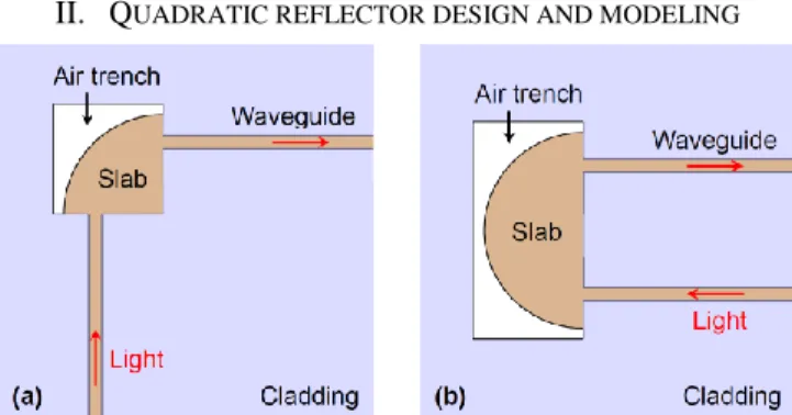
Fig. 1. Schematic top-view of (a) a 90° and (b) a 180° bend structure.
Figure 1a schematically illustrates a 90° waveguide bend layout incorporating an air-trench quadratic reflector. The waveguide core first transitions into a slab region, allowing the waveguide mode to expand in-plane in the form of a 2-D diverging beam. The waveguide and the slab region are both encapsulated in a cladding layer, and thus scattering loss at the waveguide-slab junction is negligible. The expanding beam is then total internal reflected at the slab-air interface and refocused by the reflector, transforming into a 2-D converging beam. The 2-D beam is designed to naturally match the numerical aperture (NA) and mode profile of the waveguide due to symmetry of the structure, enabling efficient coupling into the other waveguide along the orthogonal direction. In this embodiment, the reflector assumes an elliptical shape. Output from a LIC waveguide can be well approximated as light emitted from a point source. Therefore, by placing the effective “point sources” pertaining to the two waveguides at focal points and adjusting eccentricity of the elliptical reflector, the reflector
We further note that positions of the effective sources (aka the foci of the elliptical reflector) do not coincide with the waveguide facets. The offset distance between the effective point source and the waveguide facet depends on the index contrast and dimensions of the waveguide. In addition, the elliptical reflector in our design is slightly shifted along the surface normal direction to compensate for the phase shift caused by the Goos-Hanchen effect upon TIR[36], [38]. In practice, the optimized position of the reflector can be obtained by parameter-sweep full-wave simulations using the geometric optics design as a starting heuristic.
While the elliptical reflector design minimizes mode leakage, it creates an asymmetric light intensity distribution in the reflected beam which ultimately bounds the coupling efficiency[43], [44]. This limitation can be circumvented by cascading two quadratic reflectors such that the second reflector again mirrors the intensity profile and hence compensates for the asymmetry. In Fig. 1b, a 180° bend structure containing two cascaded parabolic reflectors is illustrated. In this design, the first parabolic reflector transforms the 2-D diverging beam from the waveguide into an in-plane collimated beam, and the second reflector converts the collimated beam into a converging beam precisely matching the waveguide mode. Free-form reflectors based on the aforementioned design principles can be utilized to further optimize the mode-matching and redirecting conditions, allowing high-performance arbitrary waveguide bending/routing.
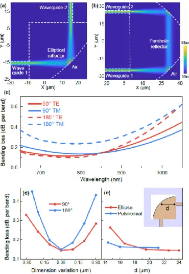
We modeled coupling efficiencies of the elliptical and parabolic reflectors using 3-D full-wave finite-difference time-domain (FDTD) simulations (Lumerical FDTD Solutions). In the simulations, the waveguide core and cladding refractive indices are chosen to be 1.543 and 1.525, respectively, to match our experimental conditions. The waveguide core has a square cross-section with 2.3 μm width/height to ensure single-mode operation near 850 nm wavelength. Using the traditional waveguide bending design, the LIC waveguide requires a bending radius of 0.8 mm or larger to obtain a bending loss of < 0.3 dB[7]. In contrast, the quadratic reflector designs exhibit broadband high optical efficiencies with radically reduced footprints as shown in Fig. 2. The peak coupling efficiencies are 97.4% (0.116 dB bending loss, TE polarization) and 96.9% (0.135 dB bending loss, TM polarization) for the 90° bend, and 97.7% (0.099 dB bending loss, TE polarization) and 94.7% (0.235 dB bending loss, TM polarization) for the 180° bend. We note that the bending losses of the 180° bend is considerably less than twice of the 90° bend losses, which we attribute to the reduced beam intensity asymmetry after two consecutive reflections. As a comparison, we also modeled the performance of air-trench bends using flat TIR mirrors with a configuration similar to that in[37]. For waveguides with identical sizes and core/cladding indices, the losses of 90° bends based on flat reflectors optimized at 850 nm wavelength are 0.58 dB and 0.32 dB for TE and TM polarizations, respectively. The significantly higher losses are largely ascribed to incomplete TIR at large bending angles, translating to limited bending capability and
compactness. Decreasing the bending angle to 45° reduces the losses per bend to 0.08 dB (TE polarization) and 0.09 dB (TM polarization), which however is still considerably larger than those of the quadratic reflectors for the same total bending angle due to the inevitable leaking of high spatial frequencies component associated with reflection on flat mirrors.
Fig. 2. (a, b) 3-D FDTD simulations showing light intensity distributions across the center plane of the (a) 90° bend and (b) 180° bend for TE polarization; (c) wavelength and polarization dependent loss of the 90° and 180° bends. (d) fabrication tolerance of TE mode at 850 nm wavelength. (e)
Fabrication tolerance of the quadratic reflectors was investigated by modeling the bending loss change with varying reflector size. The result shown in Fig. 2d suggests that 0.3-dB tolerance for the 90° and 180° bends is 400 nm and 250 nm, respectively. The large tolerance is well within reach of standard UV lithography.
It is also interesting to examine whether the quadratic design corresponds to an optimized reflector shape. We therefore designed generic curved reflectors for 90° bend using the genetic algorithm by parameterizing the curve with a polynomial up to the fifth order. The size-dependent bending loss is shown in Fig. 2e for both the elliptical reflector and the optimized polynomial curve reflector. Here the x-axis gives the distance between the waveguide facet and the reflector as a measure of the reflector size. The bending loss decreases with increasing reflector size and plateaus at about 20 µm. In all
cases except the smallest size, the two designs yield almost identical bending losses. This result demonstrates that the quadratic reflector design, herein derived from a simple ray optics argument, indeed offers a geometrically optimal solution to compact, low-loss waveguide bends.
III. DEVICE FABRICATION
Fig. 3. (a-c) Tilted-view schematics of the fabrication process: (a) after waveguide/reflector patterning; (b) after patterning of the sacrificial block; and (c) final structure; (d-f) top-view optical microscope images of the device corresponding to steps in (a-c); (g) SEM image of a 180° bend structure; (h) top-view SEM image showing the test structures used to quantify the bending losses. The images in (g) and (h) were both taken before fabrication of the sacrificial block.
In a traditional fabrication process involving air trenches, the waveguides are first defined followed by air trench etching, which necessitates precise alignment between the waveguides and air trenches. Here we demonstrate a self-aligned fabrication approach to circumvent the challenge. The basic processing steps are depicted in Fig. 3a-3c with corresponding device images shown in Figs. 3d-3f. The process starts with sequential coating of the bottom cladding (OrmoClad, refractive index n = 1.523 at 850 nm wavelength), core (OrmoCore, n = 1.543 at 850 nm), and top cladding (OrmoClad) layers following our previously established protocols[7]. A metal hard mask (Cr/Cu, 5/200 nm) was subsequently patterned using a lift-off process, followed by inductively coupled plasma (ICP) reactive ion etching (PlasmaPro 100 Cobra, Oxford Instruments) through the entire stack to define both the reflector surface and the feeding waveguides. The etching recipe (O2/CF4: 20/30 sccm, ICP/DC power: 1500/75 W, pressure: 10 mTorr, substrate temperature: 20 °C, and etch rate: 0.5 ± 0.05 μm/min) was carefully optimized to obtain a vertical sidewall angle (90° ± 0.5°). A resist layer (SPR220-7.0) was then spin coated and patterned to define a sacrificial block at the air trench location. Another OrmoClad film was coated to encapsulate the structure. Finally, a blanket shallow etch was performed to
A key feature of our process is that it does not involve precise alignment since the reflector surface and the waveguides are defined in the same patterning step. Benefiting from the relaxed alignment requirement, all patterning steps throughout the entire fabrication process were carried out on an i-line UV stepper (GCA AutoStep 200, specified resolution: 0.65 μm), fully compatible with standard high-throughput wafer-scale manufacturing.
Losses of the 90° and 180° bends were quantified using structures shown in Fig. 3h, which encompass waveguides containing 4, 8, 12, and 16 identical bends. Transmission measurements through the waveguides were performed via fiber end-fire coupling. A superluminescent diode (SLD, QSDM-860-8B, QPhotonics LLC) with an emission spectrum presented in Fig. 4a inset was used as the light source. Light was coupled into/out of the devices through lensed fiber tapers (OZ Optics), with polarization manipulated by a manual paddle fiber polarization controller, and the output was monitored using an optical spectrum analyzer (AQ-6315A, Ando) and a calibrated power meter (818-IS-1, Newport Corporation).
IV. BENDING LOSS CHARACTERIZATION RESULTS AND DISCUSSION
Fig. 4. (a) Insertion loss measured over the entire SLD spectrum as a function of number of 90° bends on the test structures, yielding fitted losses of (0.31 ± 0.02) dB and (0.30 ± 0.03) dB per bend for TE and TM polarizations, respectively; inset shows emission spectrum of the SLD source used in the measurement; (b) measured wavelength-dependent bending loss of the 90° bend.
Losses of the 90° and 180° bends were quantified using structures shown in Fig. 3h, which encompass waveguides containing 4, 8, 12, and 16 identical bends. Transmission measurements through the waveguides were performed via fiber end-fire coupling. A superluminescent diode (SLD,
was coupled into/out of the devices through lensed fiber tapers (OZ Optics), with polarization manipulated by a manual paddle fiber polarization controller, and the output was monitored using an optical spectrum analyzer (AQ-6315A, Ando) and a calibrated power meter (818-IS-1, Newport Corporation).
Fig. 5. (a) Insertion loss measured over the SLD spectrum as a function of number of 180° bends on the test structures, yielding fitted losses of (0.27 ± 0.04) dB and (0.30 ± 0.05) dB per bend for TE and TM polarizations, respectively; (b) measured wavelength-dependent bending loss of the 180° bend.
Figures 4 and 5 summarize the measurement results for the 90° and 180° bends, respectively. The data was collected from more than 40 waveguides on multiple dies. The 90° bend exhibits losses of (0.31 ± 0.02) dB for the TE polarization and (0.30 ± 0.03) dB for the TM polarization, whereas the 180° bend exhibits losses of (0.27 ± 0.04) dB for the TE polarization and (0.30 ± 0.05) dB for the TM polarization, both of which are averaged over the entire SLD emission spectrum. Notably, the bending losses of the 180° bend further decrease to 0.20 and 0.23 dB per bend at 830 nm wavelength, consistent with the simulation results in Fig. 2c. These losses can be further reduced through process optimization to correct for dimensional deviations caused by slight lateral etching during the reflector patterning process and eliminate roughness on the reflector surface. Despite the higher measured losses than our simulated values, our results are still among the lowest reported loss figures in compact LIC waveguide bends for equivalent total bending angles of 90° or 180° (Table 1).
V. CONCLUSION
In this paper, we designed and experimentally demonstrated a compact bend design based on air trench quadratic (elliptical or parabolic) reflectors in LIC polymer waveguides. The quadratic reflecting surface geometry yields minimal mode
leakage and accounts for high coupling efficiencies in the design. The design also affords broadband and polarization-insensitive operation. We further proposed a new self-aligned fabrication method to eliminate the stringent alignment requirement mandated by prior air trench designs and validated its compatibility with standard wafer-scale UV lithographic fabrication. The device architecture and fabrication route are generically applicable to other LIC systems besides polymers, qualifying our approach as a promising path towards high-density, low-loss photonic circuits.
TABLE 1.
SUMMARY OF AIR-TRENCH BEND DESIGNS IN LIC WAVEGUIDES AND EXPERIMENTALLY OBTAINED PERFORMANCES
Design Fabrication technique Bending angle Bending loss (TM) Bending loss (TE) Referen ce Air trench + offset bend UV lithography 180° 0.45 dB @ 1.4 mm bend radius [29] Planar air trench reflector UV lithography 45° 0.30 dB 0.33 dB [36] Planar air trench reflector Electron beam lithography 45° 0.17 dB 0.12 dB [37] Elliptical reflector UV lithography 90° 0.30 dB 0.31 dB This work Parabolic reflector UV lithography 180° 0.30 dB 0.27 dB This work REFERENCES
[1] R. Dangel et al., “Polymer waveguides for electro-optical integration in data centers and high-performance computers,” Opt.
Express, vol. 23, no. 4, p. 4736, 2015.
[2] R. Dangel et al., “Development of Versatile Polymer Waveguide Flex Technology for Use in Optical Interconnects,” J. Light.
Technol., vol. 31, no. 24, pp. 3915–3926, Dec. 2013.
[3] C. Choi et al., “Flexible Optical Waveguide Film Fabrications and Optoelectronic Devices Integration for Fully Embedded Board-Level Optical Interconnects,” J. Light. Technol. Vol. 22, Issue 9, pp.
2168-, vol. 22, no. 9, p. 2168, Sep. 2004.
[4] T. Gu, R. Nair, and M. W. Haney, “Prismatic coupling structure for intrachip global communication,” IEEE J. Quantum Electron., vol. 45, no. 4, pp. 388–395, 2009.
[5] M. W. Haney, R. Nair, T. Gu, R. Nair, and M. W. Haney, “Chip-Level Multiple Quantum Well Modulator-Based Optical Interconnects,” vol. 31, no. 24, pp. 4166–4174, Dec. 2013. [6] J. Missinne, S. Kalathimekkad, B. Van Hoe, E. Bosman, J. Vanfleteren, and G. Van Steenberge, “Stretchable optical waveguides,” Opt. Express, vol. 22, no. 4, p. 4168, Feb. 2014. [7] H. Zuo, S. Yu, T. Gu, and J. Hu, “Low loss, flexible single-mode
polymer photonics,” Opt. Express, vol. 27, no. 8, p. 11152, 2019. [8] A. Ródenas et al., “Three-dimensional mid-infrared photonic
circuits in chalcogenide glass,” Opt. Lett., vol. 37, no. 3, p. 392, Feb. 2012.
[9] A. Arriola et al., “Low bend loss waveguides enable compact, efficient 3D photonic chips,” Opt. Express, vol. 21, no. 3, p. 2978, Feb. 2013.
[10] T. Barwicz and Y. Taira, “Low-Cost Interfacing of Fibers to Nanophotonic Waveguides: Design for Fabrication and Assembly Tolerances,” IEEE Photonics J., vol. 6, no. 4, pp. 1–18, Aug. 2014. [11] T. Barwicz et al., “A Novel Approach to Photonic Packaging
Leveraging Existing High-Throughput Microelectronic Facilities,”
IEEE J. Sel. Top. Quantum Electron., vol. 22, no. 6, pp. 455–466,
Nov. 2016.
[12] C. Y. Chao, W. Fung, and L. J. Guo, “Polymer microring resonators for biochemical sensing applications,” IEEE J. Sel. Top. Quantum
Electron., vol. 12, no. 1, pp. 134–142, Jan. 2006.
[13] A. Maxwell, S. W. Huang, T. Ling, J. S. Kim, S. Ashkenazi, and L. J. Guo, “Polymer microring resonators for high-frequency ultrasound detection and imaging,” IEEE J. Sel. Top. Quantum
Electron., vol. 14, no. 1, pp. 191–197, Jan. 2008.
[14] L. Li et al., “Monolithically integrated stretchable photonics,” Light
Sci. Appl., vol. 7, no. 2, p. 17138, 2018.
[15] T. Meany et al., “Laser written circuits for quantum photonics,”
Laser Photon. Rev., vol. 9, no. 4, pp. 363–384, Jul. 2015.
[16] G. D. Marshall et al., “Laser written waveguide photonic quantum circuits,” Opt. Express, vol. 17, no. 15, p. 12546, Jul. 2009. [17] S. G. Johnson, M. L. Povinelli, M. Soljačić, A. Karalis, S. Jacobs,
and J. D. Joannopoulos, “Roughness losses and volume-current methods in photonic-crystal waveguides,” Appl. Phys. B Lasers
Opt., vol. 81, no. 2–3, pp. 283–293, Jul. 2005.
[18] D. M. Kita, J. Michon, S. G. Johnson, and J. Hu, “Are slot and sub-wavelength grating waveguides better than strip waveguides for sensing?,” Optica, vol. 5, no. 9, p. 1046, Sep. 2018.
[19] J. Hu et al., “Low-loss high-index-contrast planar waveguides with graded-index cladding layers,” Opt. Express, vol. 15, no. 22, p. 14566, 2007.
[20] J. Hu, L. Li, H. Lin, P. Zhang, W. Zhou, and Z. Ma, “Flexible integrated photonics: where materials, mechanics and optics meet [Invited],” Opt. Mater. Express, vol. 3, no. 9, p. 1313, 2013. [21] J. Lapointe et al., “Fabrication of ultrafast laser written low-loss
waveguides in flexible As2S3 chalcogenide glass tape,” Opt. Lett., vol. 41, no. 2, p. 203, Jan. 2016.
[22] L. Li et al., “A new twist on glass: A brittle material enabling flexible integrated photonics,” Int. J. Appl. Glas. Sci., vol. 8, no. 1, pp. 61–68, 2017.
[23] S. Aikio et al., “Disposable photonic integrated circuits for evanescent wave sensors by ultra-high volume roll-to-roll method,”
Opt. Express, vol. 24, no. 3, p. 2527, Feb. 2016.
[24] I. Papakonstantinou, K. Wang, D. R. Selviah, and F. A. Fernández, “Transition, radiation and propagation loss in polymer multimode waveguide bends,” Opt. Express, vol. 15, no. 2, p. 669, Jan. 2007. [25] F. T. Dullo, J. C. Tinguely, S. A. Solbø, and O. G. Hellesø,
“Single-mode limit and bending losses for shallow Rib Si3N4 waveguides,”
IEEE Photonics J., vol. 7, no. 1, Feb. 2015.
[26] R. Pafchek, R. Tummidi, J. Li, M. A. Webster, E. Chen, and T. L. Koch, “Low-loss silicon-on-insulator shallow-ridge TE and TM waveguides formed using thermal oxidation,” Appl. Opt., vol. 48, no. 5, pp. 958–963, Feb. 2009.
[27] P. Dong et al., “Low loss shallow-ridge silicon waveguides,” Opt.
Express, vol. 18, no. 14, p. 14474, Jul. 2010.
[28] N. Bamiedakis, R. V. Penty, and I. H. White, “Compact multimode polymer waveguide bends for board-level optical interconnects,” J.
Light. Technol., vol. 31, no. 14, pp. 2370–2375, 2013.
[29] B. Howley, X. Wang, R. T. Chen, and Y. Chen, “Experimental evaluation of curved polymer waveguides with air trenches and offsets,” J. Appl. Phys., vol. 100, no. 2, 2006.
[30] R. Pitwon et al., “Polymer optical waveguides with reduced in-plane bend loss for electro-optical PCBs,” in Integrated Optics: Devices,
Materials, and Technologies XVI, 2012, vol. 8264, p. 82640Z.
[31] M. Popović, K. Wada, S. Akiyama, H. A. Haus, and J. Michel, “Air trenches for sharp silica waveguide bends,” J. Light. Technol., vol. 20, no. 9, pp. 1762–1772, Sep. 2002.
[32] E. P. Ippen et al., “Air Trench Bends and Splitters for Dense Optical Integration in Low Index Contrast,” J. Light. Technol. Vol. 23, Issue
7, pp. 2271-, vol. 23, no. 7, p. 2271, Jul. 2005.
[33] W. Bogaerts and S. K. Selvaraja, “Compact single-mode silicon hybrid rib/strip waveguide with adiabatic bends,” IEEE Photonics
J., vol. 3, no. 3, pp. 422–432, Jun. 2011.
[34] R. K. Navalakhe, N. Dasgupta, and B. K. Das, “Fabrication and characterization of straight and compact S-bend optical waveguides on a silicon-on-insulator platform,” Appl. Opt., vol. 48, no. 31, pp. G125–G130, Nov. 2009.
[35] W. M. Pätzold, A. Demircan, and U. Morgner, “Low-loss curved waveguides in polymers written with a femtosecond laser,” Opt.
Express, vol. 25, no. 1, p. 263, Jan. 2017.
[36] J. Cardenas, L. Li, S. Kim, and G. P. Nordin, “Compact low loss single air interface bends in polymer waveguides,” Opt. Express, vol. 12, no. 22, p. 5314, 2004.
[37] Y. Lin, J. Cardenas, S. Kim, and G. P. Nordin, “Reduced loss through improved fabrication for single air interface bends in
[38] L. Li, G. Nordin, J. English, and J. Jiang, “Small-area bends and beamsplitters for lowindex-contrast waveguides,” Opt. Express, vol. 11, no. 3, p. 282, 2003.
[39] A. L. Glebov et al., “Integrated waveguide micro-optic elements for 3D routing in board-level optical interconnects,” in Photonics
Packaging and Integration VI, 2006, vol. 6126, p. 61260N.
[40] Y. Qian, S. Kim, J. Song, G. P. Nordin, and J. Jiang, “Compact and low loss silicon-on-insulator rib waveguide 90° bend,” Opt.
Express, vol. 14, no. 13, p. 6020, 2006.
[41] S. Lardenois et al., “Low-loss submicrometer silicon-on-insulator rib waveguides and corner mirrors,” Opt. Lett., vol. 28, no. 13, p. 1150, Jul. 2003.
[42] R. Orobtchouk, S. Laval, D. Pascal, and A. Koster, “Analysis of integrated optical waveguide mirrors,” J. Light. Technol., vol. 15, no. 5, pp. 815–820, 1997.
[43] Z. Hou, X. Li, Y. Huang, and S. T. Ho, “Physics of elliptical reflectors at large reflection and divergence angles I: Their design for nano-photonic integrated circuits and application to low-loss low-crosstalk waveguide crossing,” Opt. Commun., vol. 287, pp. 96–105, 2013.
[44] Z. Hou, X. Li, Y. Huang, and S. T. Ho, “Physics of elliptical reflectors at large reflection and divergence angles II: Analysis of optical beam distortions in integrated ultra-large-angle elliptical curved reflectors,” Opt. Commun., vol. 287, pp. 106–116, 2013. [45] S. Yu et al., “Seamless Hybrid-integrated Interconnect NEtwork
(SHINE),” in 2019 Optical Fiber Communications Conference and
Exhibition (OFC), 2019, p. M4D.5.
[46] Z. Wang et al., “Integrated small-sized semiconductor ring laser with novel retro-reflector cavity,” IEEE Photonics Technol. Lett., vol. 20, no. 2, pp. 99–101, Jan. 2008.
[47] Z. Wang, G. Yuan, G. Verschaffelt, J. Danckaert, and S. Yu, “Injection locking and switching operations of a novel retro-reflector-cavity-based semiconductor micro-ring laser,” IEEE
Photonics Technol. Lett., vol. 20, no. 20, pp. 1673–1675, Oct. 2008.
[48] M. Strain and M. Sorel, “Curved facet 90° turning mirrors for integrated optical technologies,” Electron. Lett., vol. 46, no. 5, pp. 360–362, 2010.