Design of Class E Resonant Rectifiers for Very High Frequency Power Conversion
by
Juan Antonio Santiago-Gonz Iez
B.S. in Electrical Engineering, University of Puerto Rico at Mayaguez, 2011
SUBMITTED TO THE DEPARTMENT OF ELECTRICAL ENGINEERING AND COMPUTER SCIENCE IN PARTIAL FULFILLMENT OF THE REQUIREMENTS
FOR THE DEGREE OF
MASTER OF SCIENCE IN ELECTRICAL ENGINEERING AT THE
MASSACHUSETTS INSTITUTE OF TECHNOLOGY
SEPTEMBER 2013
C2013 Massachusetts Institute of Technology. All rights reserved.
Signature of Author
Dep I ent of Electrical Engineering an4"Computer Science August, 30, 2013 6
David J. Perreault Professor of Electrical Engineering and Computer Science Thesis Supervisor
khurram K. Afridi Visiting Associate Professor of Electrical Engineering and Computer Science Thesis Supervisor A
- d(J eeslie A. Kolodziejski Professor of Electrical Engineering and Computer Science Chair, Department Committee on Graduate Students
ARGHNIES
Certified by
Certified by
Accepted by
Design of Class E Resonant Rectifiers for Very High Frequency Power Conversion
by
Juan Antonio Santiago-Gonzailez
Submitted to the Department of Electrical Engineering and Computer Science on August 30, 2013, in partial fulfillment of the requirements for the degree of
Master of Science
Abstract
Resonant rectifiers have important applications in very-high-frequency power conversion systems, including dc-dc converters, wireless power transfer systems, and energy recovery circuits for radio-frequency systems. In many of these applications, it is desirable for the rectifier to appear as a resistor at its ac input port. However, for a given dc output voltage, the input impedance of a resonant rectifier varies in magnitude and phase as output power changes.
In this thesis, a design method is introduced for realizing single-diode "shunt-loaded" resonant rectifiers, or class E rectifiers, that provide near-resistive input impedance over a wide range of output power levels. The proposed methodology is demonstrated experimentally for 10:1 and 2:1 power range ratios at 30 MHz input frequency. Some design limitations are found and explained. Additionally, the performance of Schottky diodes in very high frequency (VHF) rectifiers is explored. It has been found that diodes have increased losses when switched at VHF and this phenomenon varies by manufacturer and device specifications. A study of diodes in Class E rectifiers is conducted to assess their performance in VHF rectification. Some good diodes are identified for VHF operation, including both commercial Si and SiC Schottky diodes and experimental GaN diodes. The foundations are laid for developing a library of diodes useful for this application.
The resonant rectifier design methodology presented in this thesis uses a graphical approach based on normalized design curves. It enables a fast design with only a small amount of calculations needed and yields good accuracy in the final circuit. It is hoped that this design approach and the insights available from the design curves will prove to be useful in designing resonant rectifiers in applications that require resistive rectifier loads.
Thesis Supervisor: David J. Perreault
Title: Professor of Electrical Engineering and Computer Science Thesis Supervisor: Khurram K. Afridi
Acknowledgements
There are many people who have contributed to the writing of this thesis is one way or another, directly or indirectly. I would like to start by thanking my advisors David Perreault and Khurram Afridi. This work would never have been possible without your guidance and patience. You have helped me tremendously in developing as an engineer and growing as a person. You were there making sure I progressed and always lend a hand when I needed one. This learning experience has been exceptional and unique. You are great examples of what makes MIT such an amazing place.
To the MIT/MTL GaN Energy Initiative and its affiliates, including Sumitomo Electric Industries, Ltd. who provided the experimental GaN diodes, thank you for providing funding and otherwise helping with my research and the material for this thesis.
I would also like to present my gratitude to my advisors in my undergraduate institution, the University of Puerto Rico at Mayagtiez (UPRM), Baldomero Llorens and Eduardo Ortiz. You saw some potential in me and showed me the path of research and graduate school, of doing something more than getting good grades in courses, of applying textbook knowledge to the real world. Thank you for being such great mentors, I would never have made it to MIT without your help.
I would like to thank my lab mates Samantha, John, Wardah, Jorge, Seungbum, Minjie, Khalil, Alex, Lisa and Yiou and all others at LEES. You have helped me either through completing P-sets, answering research questions or just great laughs. Thank you to doctors Robert Pilawa, Brandon Pierquet, Wei Li and Juan Rivas for their help and mentoring. Also thank you to my friends Baldin, Phillip, Edward, Francine, Mely, Yamil, Enrique, Carlos, Diamy, C.J., Chelcie and all my out of work Boston friends. You guys have provided a lot of support and fun times and have a special place in my heart. To my friends in Puerto Rico, Arnold, Jay, Charlie, Carlitos, Jona, Dollian, Roberto and Jose A., I miss all of you and hope to see you soon. Thank you for giving me great memories and fun times whenever we get together. I want to also thank the MSRP people, especially M6nica, for introducing me to MIT and all of its wonders.
Last but not least, I would like to thank my parents Hector and Maritza and my brother Manolo. Thank you for raising me with much care and love and providing for my every need. You are my inspirations and I hope to be as successful as you someday. Thank you for providing me the opportunity to study and learn, but also teaching me how to be a good person and citizen. Thank you for supporting me every step of the way, for cheering me up when I was down and for believing in me. No part of this could have been made without you.
Table of Contents 1. Introduction... 14 1.1. M otivation...15 1.2. Past Work...16 1.3. Thesis O bjectives...17 1.4. Thesis Organization... 17
2. Class E Rectifier Analysis and Design...19
2.1. Class E Rectifier Operation and Analysis...19
2.2. Design Methodology Plots...25
2.3. Simulation Results...29
3. Experimental Validation of Class E Rectifier...34
3.1. Experimental Setup...34
3.2. High capacitance design...39
3.3. Near resistive input design...45
4. Low Voltage Diode Performance in VHF...51
4.1. M otivation ... 52
4.2. Experimental Setup...53
4.3. R esults... 57
5. High Voltage Diode Performance in VHF...67
5.1. M otivation ... 67
5.2. Diode Capacitance Measurement...68
5.3. Diode Performance Measurement...70
5.4. Experimental Setup ... 71
5.4.1. Capacitance Measurement...71
5.5. R esults... 76
5.5.1. Capacitance Measurement...76
5.5.2. Diode Performance Measurement...78
6. C onclusions...84
6.1. Thesis Summary...84
6.2. Thesis Conclusions...85
6.3. Future Work... 86
Appendix A Matlab Code...87
Appendix B Board Schematic and Layout Files...96
Appendix C Diode Testing Data...99
List of Figures
1.1 Typical architecture of a resonant dc-dc converter. ... 15 2.1 Class E rectifier driven by a current source...20 2.2 Class E resonant rectifier waveforms; from the top: (a) Input current, (b) diode
voltage, (c) diode current, (d) capacitor current, and (e) inductor current...21 2.3 Worst-case phase angle magnitude across the specified operating conditions vs.
normalized capacitance for different power ranges ratios (Pmax:Pmin)...26
2.4 Maximum normalized peak reverse diode voltage vs. normalized capacitance for
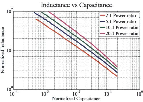
different power ranges (Pmax:Pmin)...26 2.5 Normalized inductance vs. normalized capacitance for different power ranges
ratios (P max:P min)... 27 2.6 Time-domain simulation using SPICE of the diode voltage at 18 W, 9 W and
1.8 W of output pow er...30 2.7 Time-domain simulation using SPICE of input current at 18 W, 9 W and
1.8 W of output pow er...31 2.8 Time-domain simulation using SPICE of inductor current at 18 W, 9 W and
1.8 W of output pow er...31 2.9 Resonant rectifier's simulated input impedance as a function of output
power: for 10:1 and 2:1 power range ratios: (a) input impedance phase angle
and (b) input impedance magnitude...33 3.1 Class E resonant rectifier schematic. Includes the current probe to measure the
inp ut current...35 3.2 Class E resonant rectifier rated for 15 W, 12 V output voltage and 30 MHz input
frequency ... . . 37 3.3 Block diagram of the rectifier impedance test setup...38 3.4 Oscilloscope calibration circuit input impedance. At 30 MHz the circuit looks
like a 50 K2 resistive load. All higher harmonics are effectively suppressed by the higher impedance of the circuit. Taken from the Agilent 4395 impedance
analyzer... . . .. 38
3.5 Calibration circuit voltage (dark blue) and current (light blue) waveforms.
The oscilloscope is calibrated so that the waveforms are in phase with a 50 n
3.6 Input impedance phase vs. output power with rectifier fundamental voltage measured at the diode. The red curve is the measured experimental data and the blue curve is the simulation data. The maximum absolute phase over the
specified pow er range is 30 ... 40 3.7 Input impedance magnitude vs. power output with "input" voltage measured
at the diode. The red curve is the measured experimental data and the blue
curve is the sim ulation data... 41 3.8 Diode voltage (dark blue) and input current (light blue) at full power, 15.53 W
for the circuit of Fig. 3.1 and values in table 3.1. The peak diode voltage is 42 V...41 3.9 Diode voltage (dark blue) and input current (light blue) at medium power, 5.9 W
for the circuit of Fig. 3.1 and values in table 3.1. The peak diode voltage is 32 V...42 3.10 Diode voltage (dark blue) and input current (light blue) at minimum power,
1.44 W for the circuit of Fig. 3.1 and values in table 3.1. The peak diode voltage
is 2 7 V ... 4 2 3.11 Input impedance phase vs. output power with voltage measured at the input
port for the circuit of Fig. 3.1 and values in table 3.1. The red curve is the
measured experimental data and the blue curve is the simulation data...43 3.12 Input impedance magnitude vs. output power with voltage measured at the input
port for the circuit of Fig. 3.1 and values in table 3.1. The red curve is the
measured experimental data and the blue curve is the simulation data...44 3.13 Input impedance phase vs. output power with voltage measured at the input port
with adjusted LADD for the circuit of Fig. 3.1 and values in table 3.1. The red
curve is the measured experimental data and the blue curve is the simulation data. ... 44 3.14 Input impedance magnitude vs. output power with voltage measured at the input
port with adjusted LADD for the circuit of Fig. 3.1 and values in table 3.1. The red
curve is the measured experimental data and the blue curve is the simulation data...45 3.15 Input impedance phase vs. power measured at the diode voltage node for the
circuit of Fig. 3.1 and values in table 3.2. The red curve is the measured
experimental data and the blue curve is the simulation data...48 3.16 Input impedance magnitude vs. power measured at the diode voltage node for the
circuit of Fig. 3.1 and values in table 3.2. The red curve is the measured experimental data and the blue curve is the simulation data... 48
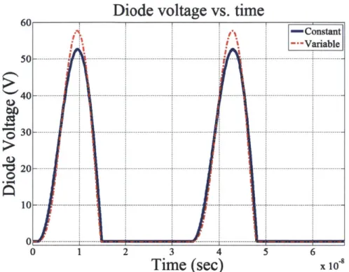
3.17 Diode voltage vs. time simulation results for a constant capacitance and for a variable capacitance. The range of the diode capacitance is 210 to 19 pF, and the constant value is 47 pF. The external capacitance is 86 pF. At higher voltage,
the variable capacitance is lower and thus the reverse voltage peaks higher...49 3.18 Diode junction capacitance vs. diode voltage for an SS 16 diode. Plotted from
a curve fit to the datasheet C-V plot...49 3.19. Diode voltage (dark blue) and input current (light blue) at full power, 12.77 W
for the circuit of Fig. 3.1 and values in table 3.2. The peak diode voltage is 60.6 V...50 4.1 Class E rectifier used to test the performance of low voltage diodes in VHF
rectification ... . . 54 4.2 Class E rectifier used to test the performance of low power diodes in VHF
rectification. On the left is the rectifier board with a dime for size scale. On the
right is the rectifier board with the input LC filter off board...56 4.3 Experimental setup block diagram...56 4.4 On the left: (a) Signal generator and power amplifier. On the right: (b) Zener
load and heatsink... 57 4.5 Diode power dissipation vs. average diode current for different diodes at 30 MHz
as tested in a class E resonant rectifier circuit with an output voltage of 12 V...58 4.6 Diode loss percentage of output power vs average diode current for different
diodes at 30 MHz as tested in a class E resonant rectifier circuit with an output
voltage of 12 V ... 59 4.7 Diode loss percentage of output power vs average diode current for different
diodes at 30 MHz as tested in a class E resonant rectifier circuit with an output voltage of 12 V. This chart shows a zoomed-in view of the performance of the
60 V diodes... 59 4.8 Diode power dissipation vs. average diode current for different diodes at 50
MHz as tested in a class E resonant rectifier circuit with an output voltage of
12 V ... ..60
4.9 Diode loss percentage of output power vs average diode current for different diodes at 50 MHz as tested in a class E resonant rectifier circuit with an output
4.10 Diode loss percentage of output power vs average diode current for different diodes at 50 MHz as tested in a class E resonant rectifier circuit with an output voltage of 12 V. This chart shows a zoomed-in view of the performance
of the 60 V diodes... 61 4.11 Diode power dissipation vs. average diode current for different diodes at 75
MHz as tested in a class E resonant rectifier circuit with an output voltage
of 12 V ... . . .. 6 1 4.12 Diode loss percentage of output power vs average diode current for different
diodes at 75 MHz as tested in a class E resonant rectifier circuit with an output
voltage of 12 V ... 62 4.13 Diode loss percentage of output power vs average diode current for different
diodes at 75 MHz as tested in a class E resonant rectifier circuit with an output voltage of 12 V. This chart shows a zoomed-in view of the performance of the
60 V diodes... ... 62 4.14 Diode power dissipation vs. average diode current for different diodes at 100
MHz as tested in a class E resonant rectifier circuit with an output voltage of
12 V ... . . 63 4.15 Diode loss percentage of output power vs average diode current for different
diodes at 100 MHz as tested in a class E resonant rectifier circuit with an output
voltage of 12 V ... 63 4.16 Diode loss percentage of output power vs average diode current for different
diodes at 100 MHz as tested in a class E resonant rectifier circuit with an output voltage of 12 V. This chart shows a zoomed-in view of the performance of the
60 V diodes... 64 4.17 Diode loss percentage of output maximum power vs frequency for the 60 V
diodes as tested in a class E resonant rectifier circuit with an output voltage
of 12 V ... . . 64 4.18. Diode voltage waveform at 50 MHz and 12.76 W output power for the Class E
rectifier. The rectifier parameters were Ls=160 nH, Cs= 64 pF, CA = 200 pF,
and Lr = 22 nH. The diode used is the SS16...65 4.19 Spice model of the SS16 diode. The simplified model includes a lead inductance
4.20. Spice simulation of diode voltage including junction capacitance and lead and
bondw ire inductance...66
5.1 Capacitance measurement circuit schematic. In the system, RBIG =10 M, and CBIG = 1 F. CBIG was a ceramic capacitor...69
5.2 Capacitance measurement circuit equivalent models. From the top: (a) dc equivalent circuit (b) ac equivalent circuit... 69
5.3 Class E resonant rectifier circuit schematic...71
5.4 Capacitance measurement circuit. Gan-SBD D is in place...73
5.5 Class E resonant rectifier circuit. The left picture shows the rectifier board with the TO-220 package diode and its heatsink. On the right the underside of the board is shown. This board was designed for through-hole devices. The diode leads were cut to reduce inductance...74
5.6 Experimental setup block diagram...75
5.7 On the left: (a) Signal generator and power amplifier. On the right: (b) Zener load and heatsink ... 75
5.8 Capacitance vs. reverse voltage curve of GaN-SBD diode A...76
5.9 Capacitance vs. reverse voltage curve of GaN-SBD diode B...77
5.10 Capacitance vs. reverse voltage curve of GaN-SBD diode C... 77
5.11 Capacitance vs. reverse voltage curve of GaN-SBD diode D...78
5.12 Diode performance plot. Diode dissipation vs. average diode current...79
5.13 Diode performance plot. Diode loss as a percentage of output power vs. average diode current...80
5.14 Diode performance plot. Diode loss as a percentage of output power vs. average diode current. Zoom in on the tail end of the plot (0.7-1.1 A)...80
5.15 GaN-SBD B. Diode voltage waveform at 57.65 W output power at 100V/div...81
5.16 GaN-SBD B. Diode voltage waveform at 57.65 W output power at 1OV/div. Zoom in on diode conduction time...82
5.17 Spice model of the GaN-SBD B diode. Includes LL, lead inductance (-10 nH), Ci, junction capacitance of the diode (33 pF), and an ideal diode. Similar to F ig . 4 .19 ... . . 82
5.18. Spice simulation of diode voltage including junction capacitance and lead and bondwire inductance...83
B. 1 Schematic of class E rectifier circuit board. Input series resistor Rsense was replaced in the final design with a loop wire for current measurement with a
clip-on current probe. Referenced in chapter 3...96 B.2 Layout of class E rectifier circuit board. The dimensions are in mm. Referenced
in chapter 3... 96 B.3 Schematic of SMD diode testing circuit board. The two inductors in parallel
provide space and versatility on the board for using multiple inductors. Only
one inductor is used at a time. Referenced in chapter 4...97 B.4 Layout of SMD diode testing circuit board. Referenced in chapter 4...97 B.5 Schematic of class E rectifier circuit board. Input series resistor Rsense was
not needed in the final design and was replaced with a wire. Referenced in chapter 5...98 B.6 Layout of class E rectifier circuit board for through hole diodes. Referenced
List of Tables
2.1 Class E Rectifier Parameter Values Used in the Simulation...29
3.1 Rectifier circuit parameters. High capacitance design... 35
3.2 Rectifier circuit parameters for a design with small external capacitance across the diode... . . 47
4.1 Diodes to be tested and their respective junction capacitance (evaluated at a bias voltage of 12 V )... 55
4.2 Rectifier circuit parameters...55
5.1 Diodes tested in class E rectifier and their capacitance at diode average voltage. All diodes rated at 500 V...73
5.2 Rectifier circuit parameters...74
5.3 Summary of Diode Performance Test...81
C. 1 Low voltage diode performance test experimental data...99
C.2 Capacitance Measurement...107
Chapter 1: Introduction
Power conversion systems are often the bottleneck in the miniaturization of electronic devices, such as laptop computers and smart phones. The size of power conversion systems is generally dominated by the size of the passive energy-storage components: inductors and capacitors, which store and release energy during each switching cycle [1,2,3]. The size of the passive energy-storage components is a function of how much energy is stored in them, which for a given level of output power is a function of the switching frequency with which energy is processed. High frequency operation of a circuit leads to energy storage components storing less energy per cycle, which in turn leads to smaller values of capacitance and inductance and thus smaller component size. Hence, to decrease size and increase power density, the power conversion circuits must operate at high frequencies. Another advantage of high-frequency operation is that air core inductors can be used if the switching frequency is high enough, thus eliminating magnetic core losses.
The limitation on increasing switching frequency comes from the increase in frequency-dependent losses, such as transistor switching losses. The switching losses can be reduced by implementing soft-switching techniques such as zero voltage switching (ZVS) [4,5], in which the switch voltage is held close to zero during switch transitions. The power conversion circuit has to be specially designed to operate efficiently under high frequency switching (e.g., see [3] and references therein). Resonant converters readily operate under ZVS conditions and high frequency leading to high efficiency and power density. Resonant power converters [4-7] are circuits that process power in a sinusoidal or quasi-sinusoidal form. Resonant dc-dc converters typically consist of an inverter stage, a transformation stage and a rectification stage, as shown in Fig. 1. Resonant rectification is the main focus of this thesis.
Transformation
Inverter stage
stage
Rectifer stage
Vin,dc _+
Vo,dc
Figure 1.1. Typical architecture of a resonant dc-dc converter.
1.1 Motivation
Resonant rectifiers have important applications in power conversion systems operating at frequencies above 10 MHz. Applications for these circuits include very-high-frequency dc-dc converters [4,5,7-12], wireless power transfer systems [8], and energy recovery circuits for radio-frequency systems [9,10]. In many of these applications, it is desirable for the rectifier to appear as a resistive load at its ac input port. For example, in some very-high-frequency dc-dc converters, proper operation of the inverter portion of the circuit can depend upon maintaining resistive (but possibly variable) loading in the rectifier stage. In still other applications it is desired to have an input impedance that is resistive and approximately constant across operating conditions [9,10]; this can be achieved by combining a set of resonant rectifiers having variable resistive input impedances with a resistance compression network [9,11,12]. In all these systems, however, it is desirable to maintain resistive input impedance of the rectifier as the operating power varies.
Resonant rectifiers have been explored in a variety of contexts [13-26]. The traditional design of a class E rectifier, or shunt-loaded resonant rectifier, utilizes a (large) choke inductor at its output and does not provide near-resistive input impedance [7,13]. This thesis introduces a design method for realizing class E rectifiers that provide near-resistive input impedance over a wide range of output power levels. The selection of a diode is also critical in very high frequency
(VHF) designs (30-300 MHz). The performance of many diodes degrades as switching
frequency increases [14], and this phenomenon is also explored in this thesis through evaluation
In summary, in realizing resonant dc-dc converters, the resonant rectifier is a very important aspect that has not been explored thoroughly at VHF frequencies. This thesis has two objectives: (i) the design optimization of the class E rectifier for near-resistive input over a wide range of power and (ii) diode performance at VHF in resonant rectifiers.
1.2 Past Work
Resonant rectifiers have been investigated in many contexts over the years [4-9,13-30]. In this thesis, we focus on the class E rectifier, or shunt-loaded resonant rectifier. Class E operation first became known through the class E inverter, a high frequency, high efficiency power amplifier requiring only a single switch and achieving ZVS [31]. Subsequently, various works on the class E rectifier were published, including its use in conjunction with the class E inverter to make dc-dc converters (e.g. [7,13,25,26]). The class E rectifier can be thought of as the counterpart of the class E inverter through "bilateral inversion" [32] or "time-reverse duality" [33] as illustrated in [7,13]. Most published works incorporating class E rectifiers have experimental results with circuits operating under 5 MHz of input ac frequency and deliver loads in the tens of watts or less [7,13, 15-23,26] (exceptions to this include [24,25]). Some designs are made specifically to operate under ZVS condition (or low DV/t during turn on) for synchronous
rectification [16,18]. Synchronous rectification is the use of an active switching device, such as a MOSFET, to perform the rectification in place of a diode. This provides control over the duty ratio and increases efficiency of the rectifier (lower forward voltage drop) but adds complexity and gating losses.
The modeling and experimental realization of most rectifiers found in the literature involve a resistive load [13, 15-17, 21-23] and a choke inductor at the output for low current ripple [7,13]. Input impedance of the rectifier is analyzed and simulated but never measured [13,17,24]. Also the effect of switching device capacitance was explored [21] and used to regulate the output voltage [22,23].
Three recent works stand out, and exemplify the need for the research and issues investigated in this thesis. The first one is a 100 MHz class E dc-dc converter [24]. The rectifier is designed to match the impedance of the inverter for optimum operation, but the circuit only operates at one power level and the overall efficiency was around 50%. The second work is a
study of the reverse recovery effect on Si, SiC and GaN diodes [27]. The tests are done on a boost converter application at 0.5, 1 and 2 MHz. Results showed that on Si diodes the reverse recovery effect has significant losses at the high frequencies considered, while the effect's losses are very small on SiC and GaN diodes.
In summary, the work presented in this thesis investigates the design of class E resonant rectifiers at HF (3-30 MHz) and VHF (30-300 MHz) frequencies. The modeling and design of such rectifiers is considered for operation to provide resistive input impedance over a wide operating power range. This is useful for the design of many kinds of dc-dc converter [9,11,12,34]. The thesis also investigates the performance of diodes for resonant rectification at VHF. The characteristics of diodes for this operating regime have not been thoroughly explored to date. Experimental performance evaluation is provided in this thesis for both commercially available diodes and select research devices.
1.3 Thesis Objective
The purpose of this thesis is to provide a methodology for designing class E rectifiers by choosing the passive components such that the input impedance of the rectifier looks near-resistive for a wide operating power range. Also, a library of diode performance in VHF resonant rectification is provided for selecting the proper switching device. By using the material in this thesis, a designer will be able to choose an appropriate diode and the rectifier inductor and capacitor for minimal input phase over a given power range. This is very useful in dc-dc converter applications and other applications where the output dc voltage is constant.
1.4 Thesis Organization
The remainder of the thesis is organized as follows: In chapter 2 we discuss the operation of the resonant class E rectifier and analyze its electrical behavior. The rectifier design method is developed and discussed thoroughly including simulation results. Chapter 3 provides the experimental validation of the design methodology. The experimental setup and procedure are discussed in detail along with experimental results. Chapter 4 explores the performance of commercially available Si Schottky diodes in resonant rectifiers at VHF. This chapter focuses on
low power devices, with a blocking voltage ranging from 60 V to 100 V and nominal current ratings of 1 A to 3 A. Results are discussed and a small library of commercially available diodes useful in VHF is developed. Chapter 5 continues the analysis started in the previous chapter but as applied to higher voltage and higher power diodes, with blocking voltages ranging from 500 V to 600 V and nominal current ratings of 4 A to 5 A. Chapter 6 concludes this work and summaries relevant findings.
Chapter 2: Class E Rectifier Analysis and Design
The class E rectifier is a single diode "shunt loaded" rectifier. In traditional designs [7,13,16], the output inductor is a choke inductor carrying dc current into a resistive load. In the design presented here, the output inductor is a resonant inductor and the output voltage is constant for all power levels (i.e., a constant-voltage load). This is appropriate to the needs of dc-dc converters [4,5,7-12] and rectifiers for energy recovery systems [9,10] among other applications.
In the following sections, the circuit operation is described and the circuit state equations are derived. These equations are used to develop a set of plots that provide a graphical method of designing class E rectifiers optimized for near-resistive input impedance over a set of pre-specified power ranges. The plots are validated with SPICE simulations.
2.1 Class E Rectifier Operation and Analysis
A class E resonant rectifier driven by a sinusoidal current source is shown in Fig. 2.1. Modeling the input source as a sinusoidal current source is appropriate for analysis purposes, as in most applications the source feeding the class E resonant rectifier is sinusoidal and/or the rectifier is provided with a high
Q (Q
> 3) series resonant tank at its input which makes thecurrent nearly sinusoidal. In the proposed design the rectifier input series resonant tank is tuned on resonance at the desired operating frequency, with a sufficiently high loaded quality factor that the input current is substantially sinusoidal. This is similar to the design of class E inverters for variable-load operation as described in [11]. Hence, for analysis the input source will be assumed to be of the form iIN = IN sin(ot + 4) where IIN is the amplitude of the input current, w its angular frequency and $ its phase. Having a non-zero phase (0) associated with the input current allows us to define the time axis in such a way that time t = 0 corresponds to the instant when the diode turns off.
The operation of the resonant rectifier is illustrated in Fig. 2.2, where we have assumed the diode to be ideal (excepting the diode capacitance, which is absorbed as part of the circuit operation). We are able to disregard the effect of the input-side resonant tank as the input current is sinusoidal and the input network is tuned on resonance. The diode turns off when
+
VD
- i i,
I
Lin
Figure 2. 1. Class E rectifier driven by a current source. Input currentiIN .5, 0 0.5 - - 1.5 I2 2.5 3 35 Diode voltage vD 70 6 0 - . .. ... ... .. ... ... .... ... ... 5 0 - . ... - ... ... ... .... ... .. ... ... 4 0 - ... ... ... ... ... 3 0 ... ... ... ... ... ... ... ... ... ... 20 . ... .. ... ... ... ... ... ... ... 10 - . .. ... ... ... .. ... ... . ... .... 0 D.5 1 1 1,5 2 2.5 3 1 3.5 le Diode currentiD In-3.5 ... ... ... ... ... ... ... ...i . .. .. .. . ... . .. .. ... . .. .. .. .. . ... ... ... ... ... ... ... ... ... ... ... ... ... ... ... ... ... ... ... ... ... ... ... ... ...... ... ... ... . ... ... ... ... ... ... ... ... ... ... ... ..... . .. .. .. ... . .. . .. .. .. .. . ... ...I ...-... . .. .. . .. .. .. .. .. .. .. I ... ... ... ... ... ... ... ... ... ... ... ... .... . ... ...7 ...... ...... ... ... ... ... ... ... ... ...... .. ...\ ... 0.5 1 1.5 5 CS
Ls
4N IL Lr+
+ VO rCA _j CrCapacitor current ic I Inutrcreti t =0 =(1- iT nt = T 3I 4 . . . . . . ... ... 1051.52 2.5 3 3.5 I Inductor current L
acrss t rts t0zra t =(1-D)T thr=T 2/) s h eido h diecretadD
Figue 2ndasuEronantrret(iie waveform so i i. . ifr from theao:()tnu urntbid voltae (c)adiodae
cuasre()capcior.Ia crtrad(e)aiyductor c sEetfnt. areidutrisue a h otu
sthttedc currenttruhiI is uNeaches zonstatt H0w)e. byAtxn this encnstathecpior aos te adiowda sutarscangizrntial current.cmoei As, wa rpesult the reveseltagf acssgin th diodse
ireasfes swly wer-itin inaudt mequale to zr.The iode trn nwhekn thned resolage, acrosspit returno er at the( -DTe atwheT= (riefreun) is the iodo he drie urntdanta,
Thpoenducftor curenotageL veform ( how inpt Fitg) 2.2 dife frmntat ofmptraditfothe
tinputre ipdnct) ofi thas rectiitude e . frnequncDi ther-tinoidof te fundamental
expression for the waveform of VD. The reverse diode voltage waveform across the full period is
given by:
VD (t)=
IJNoLr Z1
(()2 -1sin(wt) sin(P) - ir sin(ort) sin(O) + COS(Ort) cos(O) - cos(Ot) cos(4)
(gj) -_1
IVO
wLrcos(Wrt)-IINZr sin(wrt) sin(#) + VO for 0 : t (1 - D)T
0 for (1 - D)T 5 t T.
Here:
1
Wr =QLr Cr
(2)
is the resonant frequency of the Lr-C, resonant network and
Zr = (3)
is the characteristic impedance of the network.
The expression for VD contains three unknowns: diode on-state duty ratio D, input current amplitude IIN and input current phase q. The values of these unknowns need to be determined before we can compute the fundamental component of VD. For this we need to also develop an expression for the current in inductor Lr. To calculate the current, the circuit has to be analyzed in its diode-off and diode-on states. The inductor current iL when the diode is off is given by:
iL,off (t) = N [COS(Ort) sin(4) - cos(ot) sin(P)
to 2r
+ oZr sin(Wrt) cos() - sin(wt) cos(q) - sin(Ort) (4)
Zr I r
+IIN CoS(wrt) sin(q) for 0 5 t 5 (1 - D)T
and the inductor current when the diode is on is given by:
Lo(t) Vo
[
t 2ir(1- D)]Lr
6)
+ iL,off t = 2(1- D) for (1 - D)T t T. (5)
In addition, the class E rectifier circuit of Fig. 2.1 must satisfy three constraints. The first constraint is that the diode voltage VD has to be zero when the diode turns on. The second constraint is that the average value of VD has to be equal to the output voltage Vo (because the average voltage across inductor Lr is zero). The third constraint is that the average of inductor current iL has to be equal to the output power P divided by the output voltage. In summary:
VD t = 2(- D)) = 0 (6)
T 0- VD(t)dt V= , (7)
1 f T P0
iL (t) dt = . (8)
Ti0 14,
By applying these constraints to (1), (4) and (5), we can derive three independent equations in terms of the three unknowns (D, IIN and 0) and (, P, V0, Lr and Cr2:
(
sin(21T( - D)) sin(#l) - r sin 2w(1 - D))sin()) + cos 2w(i - D)) cos(#) - cos(2w(1 - D)) cos(o)
ii0 Co j 211,(1 - D)) IINZr sin&) 2wr(1 - D) sin(o) + V0 = 0 (9)
1 IIN-'r -Cos(21(1 - D)) Sin(G!) +
T
(U)27r( _ D s + ZW sin 2( - D)) cos((() cos F -CO L- 27(1 - D) sin(q5) + wcr r Wr sin(27r(1 - D)) cos(o) Vo si Wr 2rl-D W Wr (W+ IINZrCos 2r( - D) sin( ) +V0 2ir(1 - D)
IIN r -sin(!) + Zr sin(G!) + IINZr
- W2W(OrLr + sV (10)
[sin 21(l- D) sinG!)) sin(2r(1 - D)) sin(#)
1
I N to0
T 2-1G W
wLr cos Kr 2w(1 - D) cos(21( - D)) cos(#)
(OrZr W
J
+ C r 2w(1 - D) IN 2(1 - D
+ rZr
)
s r sn(0)(I2N CojLr + os() v
(g
-1 L WrZr (O ] () ,rZr)V0 27D- 2 2(1 - D) 2D\
2Lr + Loff t = (11)
These three equations, (9)-(11), can be solved numerically to find D, IIN and cP for given values of w, P0, V, Lr and Cr. These equations were coded in Matlab and solved using the fsolve function (see Appendix A. 1 for the Matlab code). This numerical approach is similar to the one used in [28-30]. The magnitude and phase of the input impedance are obtained by numerically extracting the fundamental Fourier series component of VD and comparing it to the fundamental
In this application o, V, and the maximum value of P are fixed. For a given Lr, C, pair, the code sweeps power over a given range and calculates the maximum value of phase of the input impedance. This is repeated for a range of values of Lr and Cr to determine the variation in maximum amplitude of input impedance phase with variations in values of Lr and Cr. This analysis was done for four different power range ratios (ratio of maximum to minimum power Pmax:Pmin of 2:1, 5:1, 10:1 and 20:1).
These results were used to generate a set of normalized relationships that define the values for Lr and C, that give the smallest deviation (in phase) from resistive operation over a specified operating power range ratio. This information is plotted in normalized form in three graphs (Figs. 2.3-2.5) that aid in the design of resonant class E rectifiers: (i) maximum absolute
value of input impedance phase vs. normalized capacitance, (ii) normalized peak diode reverse voltage vs. normalized capacitance, and (iii) normalized inductance vs. normalized capacitance.
The next section discusses the design of the class E rectifier using these plots.
2.2 Design Methodology
The design of the class E rectifier begins with its frequencyf(= W/27r), dc output voltage VO and output power PO specifications. These specifications can be used in conjunction with Figs.
2.3-2.5 to identify component values that minimize the worst case input impedance phase for a given power range ratio (Pmax:Pmin).
Figure 2.3 shows the absolute value of the maximum input impedance phase vs. normalized capacitance, for four different power range ratios (2:1, 5:1, 10:1 and 20:1). The capacitance is normalized as follows:
Cn = Cr 2 fV,2 (12)
PO'max
where Po,max is the maximum (rated) output power. The plot shows that to minimize the input impedance phase, the capacitance should be selected as a minimum within other design constraints (such as device voltage rating, etc.). The value of capacitance obtained with this
30 *S25 ~20 15 8 10 5 -0
Max Input Phase vs Capacitance
-2:1 Power ratio 5:1 Power ratio 10:1 Power ratio -20:1 Power ratio 0-3 102 Normalized Capacitance 10-1Figure 2.3. Worst-case phase angle magnitude across the specified operating conditions vs. normalized capacitance for different power ranges ratios (Pmax:Pmin).
Peak diode voltage vs Capacitance
10-3 10-2
Normalized Capacitance 10~1
Figure 2.4. Maximum normalized peak reverse diode voltage vs. normalized capacitance for different power ranges
(Pmaxmin). ~2 0 0 15 ~ 0 a) -2:1 Power ratio -5:1 Power ratio -10:1 Power ratio -20:1 Power ratio --- I- --- --- --- --- -- --I.. ....I. ... ... --- --- I
102 U U
I
z
10'1 100 H0Inductance vs Capacitance
---. ... ... ---- --- 2 :1 P ow er ratio -5:1 Power ratio 10: 1 Power ratio -20:1 Power ratio --- ... --- ... --- ... ... ... ... ... .... .. .. ... .... ... . . ... .... ... . . ... ... ... .. F.. ... ._ .. . . .__ .. .. .. . ... . .. . .. . . . . . . . . .. . . . .. . . .. .. . . .. 1-3 1N C0-2 Normalized Capacitance 10 1 100Figure 2.5. Normalized inductance vs. normalized capacitance for different power ranges ratios (Pma:Pmm).
methodology includes the intrinsic capacitance of the diode, any stray capacitance and any additional capacitance if needed. Hence, Cr cannot be chosen to be smaller than the intrinsic capacitance of the diode. A value of capacitance above this level should be chosen based on the acceptable value of maximum input impedance phase.
The next step is to select an appropriate diode. The required voltage rating of the diode for the selected normalized capacitance can be determined from Fig. 2.4. Figure 2.4 plots the normalized diode peak reverse voltage vs. normalized capacitance. The voltage is normalized to the dc output voltage:
VD,pk
VDf l 0
(13)
where VDpk is the diode peak reverse voltage. The normalized reverse voltage blocking capability must be greater than what is indicated by Fig. 2.4 for the selected diode. The voltage stress on the diode is reduced as capacitance increases. Hence, Fig. 2.4 gives a minimum achievable
capacitance value for a given diode peak reverse voltage rating. Once the diode is selected, one can check Fig. 2.3 to ensure that the maximum input phase of the rectifier is within acceptable limits. If not, one might want to change the diode for one with a higher voltage rating and/or lower capacitance.
The next step is to select an appropriate value of Lr. Figure 2.5 shows a plot of normalized inductance vs. normalized capacitance. The inductance is normalized as follows:
Lr
2nfPo,max
L1J=Lr (14)
From this chart one determines the appropriate value of inductance Lr that will yield the most resistive input impedance across operating power for the selected capacitance.
Finally, the input Ls-Cs filter is chosen so that the resonant frequency is equal to
f
and it provides an adequateQ
to achieve the desired spectral purity of the rectifier input waveforms for the application in question. We can quantify the relationship as:Sc = QRmin, (15)
where LS and C, are the input filter inductance and capacitance, respectively,
Q
is the quality factor of the filter and Rmin is the minimum value (at rated power) of the magnitude of rectifier input impedance Zin. The following section has a design example using this methodology that validates the approach.2.3 Design Example and Simulation Results
This section demonstrates the use of the design methodology described above in the design of a class E rectifier. The example we consider at first is that of a class E resonant rectifier operating at a frequency of 30 MHz with output voltage of 12 V dc and output power ranging from 18 W down to 1.8 W (i.e., a 10:1 power range ratio). We would like the input impedance of the rectifier to be as resistive as possible (i.e., minimize the worst-case phase angle amplitude of the input impedance) over the entire power range, while using a 60 V diode with nominal capacitance of 80 pF (based on the PMEG6020EPA diode which has average current rating of 2A). Thus, the normalized peak diode voltage capability is about 4 (assuming we allow only up to around 48 V peak with appropriate margin). From Fig. 2.4, the corresponding normalized capacitance Cn is 0.2. From Fig. 2.3 the expected maximum absolute value of input impedance phase angle is about 250. From Fig. 2.5 the normalized inductance is 3.5. De-normalizing the L and C values, the inductance Lr comes out to be 149 nH and the capacitance Cr comes out to be 132.6 pF. The value of Cr is greater than the 80 pF intrinsic capacitance of the diode. The input LC filter is designed with a
Q
of 3 and Rmin of 19 K, leading to a Cs of 93 pF and Ls of 302 nH. We also designed another rectifier with the same specifications except the power range ratio is 2:1. Only the value of L, changed to 89 nH and the expected maximum value of impedance change is 9'. Table 2.1 summarizes the design and parameters for the rectifiers to be simulated.Table 2.1. Class E Rectifier Parameter Values Used in the Simulation.
Value for 10:1 Value for 2:1 Power Range Power Range
PO 18-1.8 W 18-9 W V0 12 V 12 V f 30 MHz 30 MHz LS 302 nH 302 nH CS 93 pF 93 pF Lr 149nH 89nH Cr 132.9 pF 132.9 pF CD 80 pF 80 pF CA 52.9 pF 52.9 pF
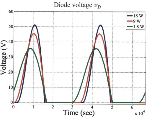
Figures 2.6-2.8 show the SPICE simulation of our designed class E rectifier using the parameters given in Table 2.1 for 10:1 power range ratio. Figure 2.6 shows the peak diode voltage to be around 51 volts, which is well within the diode specifications and well matching the predicted peak voltage of 48 V for Cn = 0.2 in this design. Figure 2.7 shows the input current
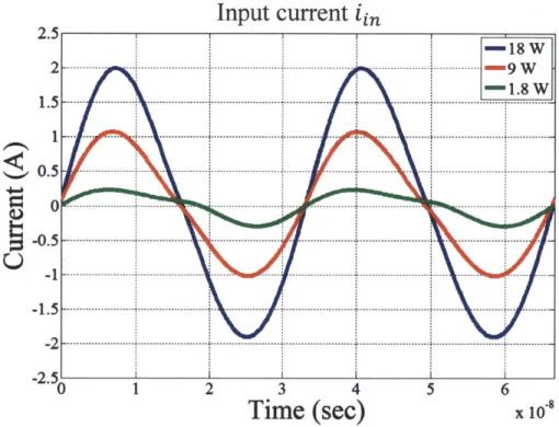
to the rectifier, which contains low harmonic content at full power and gets distorted as power decreases. Figure 2.8 shows the inductor current with substantial ac current component.
60 50 40 0 ~20 10 0 C
Diode voltage
VD -18 W -9W --- . - -- - - ---- --- - - - -----
1.8 W . - . - - - - -- ---- --- - - - --- --- - -- -- - -- ---.. ... ... . ... ... 2 3 4Time (sec)
5 6 x 10⁸ 1Figure 2.6. Time-domain simulation using SPICE of the diode voltage at 18 W, 9 W and 1.8 W of output power.
Input current ii,,
1 2 3 4 5 6
Time (sec)
x 10-8
Figure 2.7. Time-domain simulation using SPICE of input current at 18 W, 9 W and 1.8 W of output power.
Inductor current iL
2.5 2 1.5 1 0.5 0 -0.5 -1 -1.5 -2 18 W ... --- --- --- ... --- ... -9W 1.8 W --- ... ... ... I ... .... ... ... ... --- --- --- --- ... ... ... ... --- .. ... ---_--- --- ... ... .. .... --- ---... --- --- - --- ... --- --- --- ... ---... ... . ---... ... r ... I . . ... ... ... ... --- --- ... ... ... ---... .. ... .--- ... --- ---... --- T ... ... -18 W -9W --- --- T ... 1.8 W --- ... ... ... ... ... ... ... ... ---_---- -... ... ... ... ... ... ... ... ... ... . ... ... ... I ... ... ... ... ... ... -- --- ... --- -- -- ---- --- --- ... ... ... ---.... ... ... --- --- ... .. ... ... ... ... ... ... ... --- ... ... ... ---2.5 2 1.5 1 0.5 0 -0.5 0 1 2 3 4 5 6Time (sec)
x
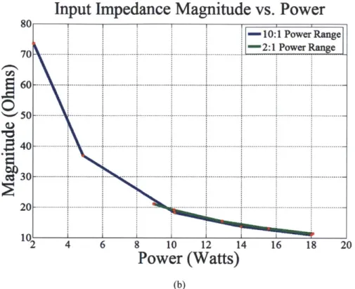
10-8Figure 2.9 shows the phase and magnitude of the input impedance of the rectifier for 10:1 and 2:1 power range ratios. The impedance magnitude is inversely proportional to output power. The impedance is capacitive at high power and becomes inductive at low power. The maximum input impedance phase amplitude found by time-domain simulations across the specified operating power range is very close to the 220 predicted by the design graph in the 10:1 power range ratio. The 2:1 power range ratio curve has a maximum impedance phase of 10' which is in close agreement with the predicted 9'. The simulated results show that our design procedure works accurately, at least for idealized diode characteristics. It also shows that it is easier to get near resistive input impedance behavior for smaller operating power range ratios.
Input Impedance Phase vs. Power
-10:1 Power Range ...--- ...- . . --- --- - - 2:1 Power Range --- -- - ---- ---- ---4 6 8 10 12 14
Power (Watts)
16 18 20 (a) 15 10 0 -2 5 Cl-10 -4-15 -20 I 2 -25Input Impedance Magnitude vs. Power
80 70 60 050 ~40 ce 30 20 10 4 16 18 20 (b)Figure 2.9. Resonant rectifier's simulated input impedance as a function of output power: for 10:1 and 2:1 power range ratios: (a) input impedance phase angle and (b) input impedance magnitude.
-10:1 Power Range -12:1 Power Range -- ---- -- -P- .-- -e --... ... .. ... .--- ---- --- - -.... -. -- --- -- -- --- -- - ---- --- - - - + --- --- ---- -4 6 8 10 12 1
Power (Watts)
Chapter 3: Experimental Validation of Class E Rectifier
In the previous chapter a methodology was introduced for designing class E rectifiers to provide near-resistive input for across a range of operating power levels. The design methodology minimizes the worst case value of input impedance phase for a specified power range ratio. It can likewise be used to maximize the power range ratio that can be achieved for a desired maximum amount of input impedance phase variation. This is useful in many applications, such as in developing dc-dc converters where it is desired to load the inverter stage with a rectifier that appears near resistive across a range of operating conditions.
In this chapter the design methodology will be validated experimentally with several designs. As the design methodology assumes a constant (linear) device capacitance, the effects of the diode non-linear junction capacitance on the design approach will be explored. Section 3.1 explains the experimental setup for the rectifier test, while sections 3.2 and 3.3 present and discuss the experimental results for high capacitance and near-resistive designs, respectively.
3.1. Experimental Setup
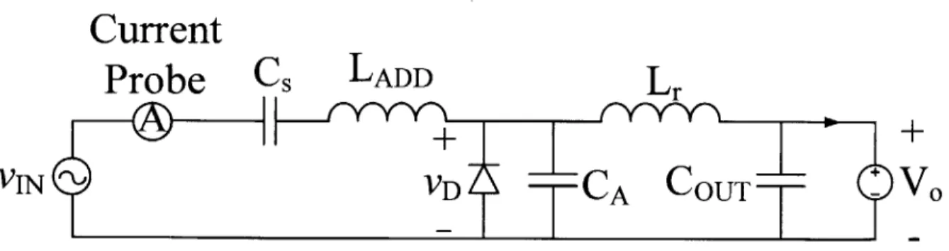
The class E resonant rectifier was designed using the methodology presented in chapter 2. Figure 3.1 shows the schematic of the class E rectifier. A wire and a current probe are added at the input to measure the input current. A TCP0030A 120 MHz current probe is used to measure the current. The inductance added by the current probe is used as part of the input filter inductance Ls. An additional inductance LADD iS introduced to achieve the value of Ls. The
cathode-to-anode (ground) voltage of the diode vD is measured with an oscilloscope using a 500 MHz, 3.9 pF TPP0500 voltage probe.
The circuit parameters are input frequency of 30 MHz, output voltage of 12 V, maximum output power of 15 W and a 10:1 power range ratio. The diode used is an SS16 from Vishay. This diode is rated at 60 V of peak reverse voltage and 1 A of average forward current. The diode capacitance was approximated to be a constant 47 pF. This value is obtained from the device datasheet's capacitance-voltage (C-V) curve for the average diode voltage in this circuit (i.e., the output voltage).
Current
Probe
Cs
LADDLr
+
+
VIN VD CA
COUT
T
Vo
Figure 3.1. Class E resonant rectifier schematic. Includes the current probe to measure the input current.
Table 3.1. Rectifier circuit parameters. High capacitance design.
Parameter Design Value Circuit Implementation
PO 15-1.5 W 15-1.5 W Vo 12 V 12-13 V 1 Ox SMBJ5349B in parallel
f
30 MHz 30 MHz Ls 307nH 306nH LProbe 60 nH (approx.)Wire and current probe
LADD 246 nH
_DD _Coilcraft
MAXI
SpringCs 91 pF 91 pF
ATC 600S
Lr 51 nH 48 nH
Coilcraft MIDI Spring
Cr 477 pF 477 pF CD 47 pF 47 pF Vishay SS16 CA 430 pF 430 pF ATC 100B COUT 20 tF 20 pF TDK Ceramic Cap
The first circuit is built to validate the design methodology under ideal conditions so is designed with a big shunt capacitance CA to minimize the effect of the diode capacitance variability. The total Cr chosen to be 477 pF, which is about ten times the diode effective capacitance, and this means CA is 430 pF. The input filter was tuned at 30 MHz with a
Q
of 3. Following the procedure described in chapter 2, for a 12 V output, maximum output power of 15 W, a power range ratio of 10:1, and a total rectifier capacitance of 477 pF, we get a rectifier inductance of L,= 50 nH. For this design, the expected maximum phase is predicted to be about 300 over a 10:1
power range ratio (from 1.5 W to 15 W), with a maximum of peak diode voltage predicted to be 38 V. Table 3.1 summarizes the rectifier parameters and Fig. 3.2 shows the rectifier circuit board. (The layout files for the circuit board are provided in Appendix B.1 and B.2.)
Figure 3.3 shows the block diagram of the experimental setup for determining input impedance. The rectifier is driven by a power amplifier (ar 150Al00B) with a sinusoidal input from a signal generator (BK Precision 4087). The load of the rectifier is a zener bank that consists of 10 SMBJ5349B diodes connected in parallel and mounted to a heat sink. The output dc voltage and current are measured with multimeters (Agilent U3606A and 34401A), the rectifier voltage is measured with a (lOx, 500 MHz) oscilloscope probe model TPP0050, and the rectifier input current is measured with the TCP0030A current probe.
The effective rectifier impedance is defined as the complex ratio of rectifier fundamental input voltage vIN to rectifier fundamental input current iIN. The input impedance is found by measuring the input voltage and current at different output power levels, extracting the fundamental frequency component of each signal through Fourier analysis in MATLAB, and taking the ratio of the two. (It is noted that the rectifier input voltage and the diode voltage ideally have the same fundamental, as the input tank is tuned on resonance. As described below, in some cases input impedance is estimated using measurements of diode fundamental voltage as the "input" voltage.). The ratio of the fundamental voltage amplitude to fundamental current amplitude is the magnitude of the impedance and the phase shift between the fundamental voltage and current signals is the impedance phase. In order to measure the phase accurately, it is important that the oscilloscope and its probes are calibrated and deskewed with good precision before each test. The oscilloscope used is a Tektronix MSO 4054B, the current probe is the TCP0030A and the voltage probe is the TPP0500. The delay between the probes needs to be adjusted (deskewed) to get an accurate phase measurement.
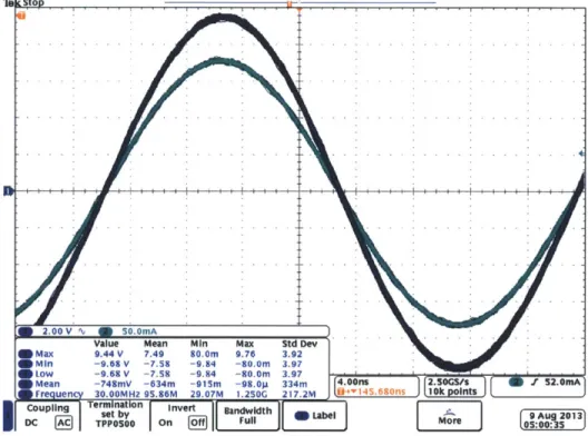
A circuit that aids in calibrating the oscilloscope was developed. The circuit was built on a similar board to the rectifier and consists of the same input LC filter of the rectifier (including the current probe) with a 50 f RF load. The circuit was tuned appropriately at the fundamental switching frequency so that at 30 MHz the impedance seen at the input is a pure 50 9 resistive load. Figure 3.4 shows the impedance measurement of the calibration circuit. The calibration circuit is connected to the power amplifier and driven by a small amount of power and the delay on the current and voltage probes is adjusted so that the signals overlap and have zero phase shift between them. This sets the scope to the zero phase or resistive impedance: any variation on the phase will be caused by the rectifier circuit. The next section discusses the experimental results.
Figure 3.2. Class E resonant rectifier rated for 15 W, 12 V output voltage and 30 MHz switching frequency.
Signal
Oscilloscope,
Generator
I-V probes
RF Power
Rectifier
Zener bank
Amplifier
board
load
DC Voltage
and Current
meter
Figure 3.3. Block diagram of the rectifier impedance test setup.
CHI IZI 50 a/ REF 100 a 50.019 a
. . . ... .. . 15 . . HZ ... ... ... ... ... .. .... . ... .. ... . .. ... C? --- --- --- - -.---...-- --CH2 Bz 5.085 / REF 0 * -52.42 m ... ... ... ... .... ... ... .. .. C ? . .. . . .... ... .. ... . . ... .. .. . ... . .. .. IF BW 1 kHz POWER 6 dBm SP 12 e START 1 MHz STOP 166 M1Hz
Figure 3.4. Oscilloscope calibration circuit input impedance. At 30 MII-z the circuit looks like a 50 Q resistive load. All higher harmonics are effectively suppressed by the higher
3.2. High capacitance design
The waveforms of the calibration circuit are shown in Fig. 3.5. The delay between the voltage and current probe was adjusted to get zero phase with a resistive load. The input impedance of the rectifier was measured using voltage measurements in two places: at the diode (assuming no phase contributions by the input LC filter) and at the input of the rectifier (including the filter). Ideally the fundamental voltage measured at these two locations should be nearly identical, as the input tank is (ideally) tuned on resonance. One measurement is done to prove the theory developed in chapter 2 with the experimental data, and another measurement is made as in a real application that includes filtering. The data is measured with the oscilloscope and processed in Matlab for fundamental frequency component extraction. (The code for this is provided in Appendix A.2)
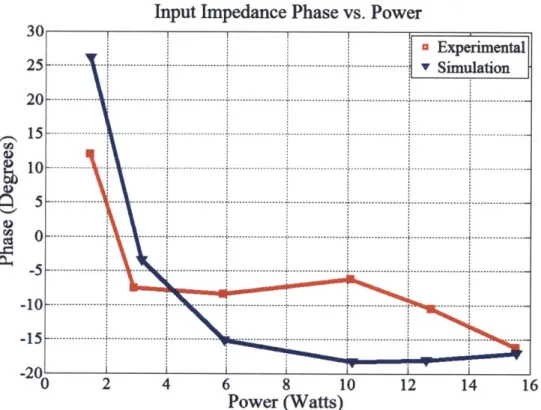
Figure 3.6 shows a plot of the impedance phase vs. power and Fig. 3.7 plots the measured impedance magnitude vs. power. Simulation results are also plotted; the simulation is ideal, including only a linear device capacitance of 47 pF, and does not include parasitic inductances, diode forward drop, output voltage increase with power due to zener diode impedance or other non-idealities. The plot shows that the maximum impedance phase is 300, which confirms our expected value from the design plots in chapter 2 (predicted values of 30' for operation from 1.5 W to 15 W).
Figure 3.8 is a screenshot of the diode voltage and input current at full power. The peak diode voltage is 42 V, which is very close to the value of 38 V predicted using Fig. 2.4 in chapter 2 for this design. It is suspected that this small deviation is due to the increase in output voltage (above 12 V) owing to the nonzero impedance of the zener bank load. A simulation that includes the output voltage increase to 13 V at full power shows the peak diode voltage is increased to 40 V. This confirms our expected value of peak diode voltage based on the design plots from chapter 2. Figs. 3.9 and 3.10 show the diode voltage and input current waveforms for 5.9 W and