Electrothermal Design and Realization of High Efficiency
Class F Power Amplifier
by
Mustafa ELARBI
THESIS PRESENTED TO ÉCOLE DE TECHNOLOGIE SUPÉRIEURE
IN PARTIAL FULFILLEMENT FOR A MASTER’S DEGREE
WITH THESIS IN ELECTRICAL ENGINEERING
M.Sc.A.
MONTREAL, AUGUST 27th, 2018
ÉCOLE DE TECHNOLOGIE SUPÉRIEURE
UNIVERSITÉ DU QUÉBEC
This Creative Commons licence allows readers to download this work and share it with others as long as the author is credited. The content of this work can’t be modified in any way or used commercially.
BOARD OF EXAMINERS
THIS THESIS HAS BEEN EVALUATED BY THE FOLLOWING BOARD OF EXAMINERS
Mr. Ammar Kouki, Thesis Supervisor
Department of Electrical Engineering at École de technologie supérieure
Mr. François Gagnon, President of the Board of Examiners
Department of Electrical Engineering at École de technologie supérieure
Mr. François Blanchard, Member of the jury
Department of Electrical Engineering at École de technologie supérieure
THIS THESIS WAS PRENSENTED AND DEFENDED
IN THE PRESENCE OF A BOARD OF EXAMINERS AND PUBLIC
AUGUST 22th, 2018
ACKNOWLEDGMENT
I would like to express my sincere gratitude to my advisor Prof. Ammar Kouki for his valuable supervision, support and encouragement throughout this thesis study.
I would also like to thank Libyan ministry of defence for their financial assistance during my graduate study. I am grateful to work for an organization where scientific research is part of product development.
I present my special thanks to Mr. Normand Gravel for sharing his precious experience. With his suggestions Mr. Normand has helped me for my first steps in LACIME and made me develop perspective in power amplifier design.
Thank you to all my friends and family, especially my mother. This thesis wouldn't have been possible without your prayers. You made me believe that it was possible to make this project and did support me on the toughest moments. I'm grateful to you... Thank you! Lastly, I would like to express my sincere thanks to my wife for here understanding and support during this work.
ELECTROTHERMAL DESIGN AND REALIZATION OF HIGH EFFICINCY CLASS F POWER AMPLIFIER
Mustafa ELARBI
RÉSUMÉ
Avec l'utilisation et la popularité croissantes des téléphones mobiles, des ordinateurs portables et des dispositifs mobiles électroniques similaires, il existe un besoin croissant de vitesses opérationnelles plus rapides. En même temps, des quantités croissantes d'énergie sont utilisées et demandées. Comment répondre à ces besoins croissants grâce à une durée de vie plus longue de la batterie est actuellement un axe majeur de recherche.
Les amplificateurs de puissance (AP) des appareils sans fil provoquent des problèmes sans fin pour les utilisateurs d'équipement de télécommunications sans fil en raison de leur consommation d’énergie très importante. Les chercheurs étudient également des moyens d'augmenter l'efficacité de la puissance opérationnelle ajoutée (PAE) dans les amplificateurs, ce qui réduit la quantité de puissance dissipée. La PAE change l'alimentation DC en RF. Par conséquent, quand le PAE est amplifié, les appareils sans fil peuvent tirer la même quantité d'énergie même en consommant moins. Les AP non linéaires de classe F et de classe F inverse, qui ont une réputation bien méritée pour leurs niveaux élevés de production d'électricité et leurs PAE, présentent un intérêt particulier pour les chercheurs. La Classe-F améliore la PAE en contrôlant le contenu harmonique.
Advanced Design System (ADS) d'Agilent a etê utilisé dans les simulations et les travaux de conception. le modèle CGHV1J006D de transistor à haute mobilité électronique a etê utilisé dans la campany de modèle de Cree (HEMT). Un PA à haute efficacité a été construit en utilisant la technologie LTCC sur un Ferro A6M. Les harmoniques d'entrée et de sortie sont toutes deux contrôlées, tandis que le réseau de forme d'onde d'entrée détermine la forme des ondes à la grille. De plus, en arrêtant les harmoniques en utilisant des terminaisons appropriées réglées en sortie, nous obtenons une forme d'onde de tension carrée et une forme d'onde demi-sinusoïdale près de la borne de drain du transistor. Les espaces partagés par les formes d'onde de courant et la tension peuvent également être réduits en taille, tout comme la consommation d'énergie du dispositif actif.
Le résultat consiste à pouvoir faire fonctionner un périphérique à 5,7 GHz avec une PAE de 54,63% et une puissance de sortie de 36,25 dBm. De plus, une nouvelle méthode d'analyse de fiabilité thermique basée sur ANSYS est également proposée pour évaluer la caractéristique thermique de l’AP. Nous avons utilisé des matériaux à haute conductivité thermique comme un alliage de cuivre et de diamant pour dissiper la chaleur dans l’environnement ambiant.
Ce travail démontre la capacité de la Classe F à améliorer considérablement le PAE en bloquant les puissances des deuxième et troisième harmoniques délivrées à la charge et en s'assurant que les formes d'onde sont formées près des bornes du transistor.
ELECTROTHERMAL DESIGN AND REALIZATION OF HIGH EFFICINCY CLASS F POWER AMPLIFIER
Mustafa ELARBI
ABSTRACT
With the increasing widespread use and popularity of cell phones, laptops and similar electronic mobile equipment, there is a subsequent rising need for faster operational speeds. At the same time, increasing amounts of energy are both being used and demanded. How to satisfy these growing needs through longer battery life is currently a major focus of research.
Power amplifiers (PAs) on wireless devices are causing endless problems for users of wireless telecommunication equipment due to their drain on the power system. Researchers are also looking into ways to increase the operational power-added efficiency (PAE) in amplifiers, this leads to reduce quantity of dissipated power. PAE changes DC power into RF, so when PAE is amplified, wireless devices can draw the same level of energy even while consuming less. Of particular interest to researchers are the non-linear class-F and class F invers PAs, which have a deserved reputation for their high levels of energy output and exceptional PAE. Class-F enhances PAE through the control of harmonic content. Agilent’s Advanced design system (ADS) can be applied in the performance of simulations and desing work. Cree’s compagny provided the ADS model of Cree’s CGHV1J006D high elcton mobility transistor (HEMT). A high efficiency PA was built using LTCC technology on an Ferro A6M. Both the input and output harmonics are controlled, while the input wave-shaping network dictates the shape of waveforms at the gate. Furthermore, in stopping harmonics using suitable terminators positioned at the output, we get a square voltage waveform and a half-sine current waveform near the transistor drain terminal. The spaces shared by the current waveforms and the voltage can also be reduced in size, as can the energy use of the active device.
The outcome was the ability to run a device at 5.7GHz on a PAE of 54.63%, and 36.25dBm output power. In addition, a novel thermal reliability analysis method based on ANSYS is proposed also to evaluate PA thermal characteristic. We used some materials have high thermal conductivity like a Cupper Diamond to dissipate the heat to the ambient
This work demonstrates Class-F PA’s ability to radically improve PAE by stopping the second and third harmonic powers delivering to the load and by having the waveforms shaped near the transistor terminals.
TABLE OF CONTENTS
Page
INTRODUCTION ...1
CHAPTER 1 POWER AMPLIFIER FUNDAMENTALS ...7
1.1 Introduction ...7
1.2 Basic Parameters ...7
1.2.1 Distortion Parameters ... 11
1.2.2 Harmonic Distortion ... 12
1.2.3 Gain offset (AM/AM) and Phase Distortion (AM/PM) ... 13
1.2.4 Power Amplifier Classes... 14
1.2.4.1 Class A Power Amplifier ... 14
1.2.4.2 Class B Power Amplifier ... 15
1.2.4.3 Class AB Power Amplifier ... 16
1.2.4.4 Class E Power Amplifier ... 17
1.2.4.5 Class F Power Amplifier ... 19
1.2.5 Quality Factor For RCL ... 27
1.3 Power Amplifier Circuit Blocks ...28
1.3.1 Stability Network ... 29
1.3.2 Matching Networks ... 31
1.3.3 Bias Network ... 32
1.4 Literature review: ...35
CHAPTER 2 ELECTRICAL DESIGN OF CLASS F POWER AMPLIFIER ...37
2.1 Introduction ...37
2.2 Requirements ...37
2.3 Device selection ...38
2.4 LTCC Technology and Material Selection ...39
2.5 Bias Network ...41
2.6 Transistor Analysis Using Nonlinear Model ...42
2.6.1 DC Analysis ... 43
2.6.2 S-parameters Verification ... 44
2.6.3 Stability Analysis and Stabilize The Transistor ... 46
2.7 Power Amplifier Design ...51
2.7.1 Multi Harmonicas Source-Pull and Load-Pull Analysis ... 51
2.7.2 Wave Shaping Networks... 54
2.7.2.1 Output Matching Network ... 55
2.7.2.2 Input Matching Network ... 56
2.8 Simulation Results ...57
2.8.1 One Tone Simulation of Power Amplifier ... 59
2.8.2 Two Tone Simulation of Power Amplifier ... 62
2.8.3 Modulated Signal Analysis of Power Amplifier ... 63
CHAPTER 3 THERMAL DESIGN OF CLASS F POWER AMPLIFIER ...67
3.1 Introduction ...67
3.2 Thermal Analysis ...69
3.2.1 Mechanical Housing ... 69
3.2.2 Thermal Simulation ... 69
3.2.2.1 Option 1: Thermal Analysis With Active Device ... 70
3.2.2.2 Option 2 : Thermal Analysis When Active Device Attached to The Materials ... 71
3.2.2.3 Option 3: Thermal Analysis With Heat Sink ... 72
3.3 Result Discussion And Comparison ...74
CHAPTER 4 REALIZATION AND MEASURMENTS ...77
4.1 Introduction ...77
4.2 Prototyping ...77
4.3 Description Of Measurements Setup ...78
4.4 CW Fundamentals Measurements ...80
4.4.1 Small Signal Measurements Results ... 80
4.4.2 Measurements of PAE, Drain Efficiency and Gain ... 81
4.5 Result Discussion ...84
CONCLUSION…… ...87
FUTURTE WORK ...88
LIST OF TABLES
Page
Table 2.1 PA Requirements ...38
Table 2.2 Some properties of semiconductor materials ...38
Table 2.3 Rogers A6M Material Properties ...40
Table 2.4 Simulated s-Parameters with VDS=40V,VGS=-2.65,IDS=30mA ...45
Table 2.5 Simulated s-Parameters with VDS=40V,VGS=-2.5,IDS=60mA ...46
Table 2.6 Input and output impedances ...54
Table 3.1 Summarizes the thermal simulation for all options. ...75
Table 4.1 Bias voltage and current values ...80
LIST OF FIGURES
Page
Figure 1. 1 Basic operation of a power amplifier ...8
Figure 1. 2 Input power, output power and power gain relation of a typical amplifier… ...9
Figure 1. 3 Power amplifier parameters ...10
Figure 1. 4 AM/AM and AM/PM characteristics of a typical PA ...13
Figure 1. 5 Input and output waveforms of class A power amplifiers ...15
Figure 1. 6 Input and output waveforms of class B power amplifiers ...16
Figure 1. 7 Transfer characteristics, voltage and current waveforms of Class AB PAS… ...16
Figure 1. 8 Bias points and voltage / current waveforms for classes A, B and AB ...17
Figure 1. 9 Circuit diagram for Class E amplifiers ...18
Figure 1. 10 Drain current, capacitor current, and drain voltage waveforms of Class E…. ...19
Figure 1. 11 Drain voltage and current waveforms of Class E ...19
Figure 1. 12 Voltage waveform (blue) and current waveform (red) ...20
Figure 1. 13 Drain voltage (left) and current (right) waveforms ...22
Figure 1. 14 Invers Class F voltage and current waveforms ...23
Figure 1. 15 The classes F and inverse Class F amplifiers ...24
Figure 1. 16 3rd Harmonic peaking configuration using lumped elements ...25
Figure 1. 17 Class F drain voltage and current waveform of 3rd harmonic peaking configuration blue – 1st harmonic / red – 3rd harmonic cyan – 2nd harmonic/green ...26
Figure 1. 18 Example of 3rd Harmonic peaking configuration ...27
Figure 1. 20 Stability network topologies ...31
Figure 1. 21 Single, open stub matching network ...32
Figure 1. 22 A typical lumped element gate and drain bias networks ...33
Figure 1. 23 A typical distributed bias network with short circuit capacitor ...34
Figure 1. 24 A typical distributed bias network with butterfly stub ...34
Figure 2.1 The CGHV1J006D GaN Transistor (a) physical photo (b) ADS model ....39
Figure 2.2 Substrate layers ...40
Figure 2.3 Design of bias network with a quarter wave and stub ...41
Figure 2.4 Resulting high impedance value for center frequency from simulation ...42
Figure 2.5 ADS schematic for determining DC bias condition of PA ...43
Figure 2.6 IV curves of the transistor ...44
Figure 2.7 The k-factor and maximum available gain ...47
Figure 2.8 Input and output stability circles ...48
Figure 2.9 Proposed ideal stability network ...48
Figure 2.10 k-factor and maximum available gain with ideal network ...49
Figure 2.11 3D capacitor ...50
Figure 2.12 Simulation result of figure 2.9 ...50
Figure 2.13 The PAE contours and the output power contours as the results for step 12.. ...53
Figure 2.14 Block diagram of input and output matching network ...54
Figure 2.15 Output matching network ...55
Figure 2.16 Output matching network response ...56
Figure 2.17 Detailed input matching network ...56
Figure 2.18 Input matching network response ...57
XVII
Figure 2.20 Simulated small signal parameters ...59
Figure 2.21 Output power, PAE (%) and power gain at 25 dBm input power ...60
Figure 2.22 Simulated second and third harmonic distortion ...60
Figure 2.23 Drain voltage (red) and current (blue) waveforms ...61
Figure 2.24 Output power versus input power...61
Figure 2.25 Input, output and DC power ...62
Figure 2.26 Intermodulation products of two tone simulation ...63
Figure 2.27 QPSK source schematic and power amplifier ...64
Figure 2.28 Layout of the power amplifier ...66
Figure 3.1 Typical thermal stack-up ...68
Figure 3.2 Power amplifier house ...69
Figure 3.3 Schematic drawing of each layer for the simulation model ...70
Figure 3.4 Thermal simulation of the PA with only the active device ...70
Figure 3.5 The relationship between the temperature and time at case1 ...71
Figure 3.6 Thermal simulation of the PA with all layers. ...71
Figure 3.7 The relationship between the temperature and time case 2 ...72
Figure 3.8 Thermal simulation of the PA with circular plate heatsink ...72
Figure 3.9 The relationship between the temperature and time in case 3 ...73
Figure 3.10 Thermal simulation of the PA with rectangular plate heatsink. ...73
Figure 3.11 The relationship between the temperature and time case 3 ...74
Figure 4.1 Fabricated Power Amplifier ...78
Figure 4.2 Wire bound connection...78
Figure 4.3 Measurements setup of fabricated PA ...79
Figure 4.5 Small signal S-parameters of the fabricated PA in CW ...81
Figure 4.6 PAE and drain efficiency ...82
Figure 4.7 The gain of PA...82
Figure 4.8 PAE and output power...83
Figure 4.9 1-dB compression point ...83
LIST OF ABREVIATIONS
PAE Power add efficiency
HEMT High electron mobility transistor
CMOS Complementary metal–oxide–semiconductor RF Radio frequency
LNA Low noise amplifier DC Direct current PA Power amplifier
TWTA Travelling wave tube amplifier GaN Gallium nitride
SiC Silicon carbide GaAs Gallium arsenide
WiMAX Worldwide Interoperability for Microwave Access Pout Output power
Pin Input power
Pdc Direct current power AM Amplitude modulation PM Phase modulation HD Harmonic distortion CCA Current conduction angle ZVS Zero voltage switching DB Power ratio in decibels ADS Advanced design system
VGS Voltage between gate and source VDS Voltage between drain and source LTCC Low temperature co-fired ceramic HFSS High frequency structure simulator AuSn Gold Tin
NA Network analyzer
IMD Intermodulation Distortion PEP Peak Envelope Power
ACPR Adjacent Channel Power Rejection QPSK Quadrature phase shift keying
INTRODUCTION
Today’s globally-interrelated telecommunication technology is at the forefront of optimization research. The arrival of smart phones and related mobile equipment on the consumer scene marked a major turning point in the evolution of advanced technology; it also radically altered how users engage with their devices. Instead of having to use multiple pieces of equipment for activities such as texting, internet browsing, and online gaming, consumers now had the means, through their Internet-connected phones, to do everything they wanted to do on just one mobile device.
There is a catch, though – along with a growing need for faster and faster Internet speeds, there was also an equally urgent need for longer battery life. The exponential increases in data transfer rates meant that exponential amounts of energy were being used to power cellular network infrastructure, and batteries were reflecting the usage by draining at faster rates. The focal point of this present research is boosting the efficacy of power-added efficiency (PAE). The entrance of digital circuits onto the telecommunications stage, along with low-power CMOS, meant that digital signals could be delivered faster and with less energy use. Unfortunately, the front-end RF equipment in the devices (e.g., low-noise amplifiers [LNA] as well as power amplifiers) is known as an energy hog that consumes immense quantities of available power in the system.
Given this situation and considering the increasing consumer demand for more effective energy use, taming the PAE of power amplifiers is offered as a solution. Furthermore, Class F and inverse Class F PAs show the most promise in our quest due to their ability to provide extreme levels of energy while at the same time providing outstanding power efficiency (i.e., higher than 80%), which is accomplished by managing the amplifiers’ harmonic content.
Microwave power amplifiers (PAs) change DC power from lower/moderate to high microwave power through the generation of current waveforms, large voltages and high frequency. In fact, microwave PAs serve as essential components in high-frequency systems such as radars,(Skolnik,2002) and wireless communications devices e.g., microwave heaters
and cellular phones,(Osepchuk,2002). Since its introduction in the early 20th century,
microwave power first used magnetrons, followed by travelling wave tube amplifiers (TWTAs) and klystrons, which function by moving electrons within a low-pressure area, (Pozar,1998). The adoption of silicon bipolar 3-terminal transistors mid-century positioned solid-state equipment at the forefront of amplifier development mainly because it was easy to implement and was also more reliable. Further advances led to the adoption of solid state in semiconductor materials such as GaN, SiC, InP and GaAs for high frequency signal spectrum areas, (Frederick et al,2003), while cost-efficiency, sizing and ease of use of the technology also gradually improved across the semiconductor industry.
Today, high-power kW- to MW-range amplifiers still mainly use TWTAs, but they are slowly being replaced by semiconductors that provide high power density. So, for instance, while GaAs equipment (in use over the past 30 years) provides around 1 W/mm at 10 GHz, GaN transistors provide >5 W/mm power density at 10 GHz. The insignificant increase in power density offered by semiconductor equipment points to the possibility of solid-state transistors likely replacing TWTAs for applications in the high microwave power sector.
Compared to traditional Si devices or GsAs, Gan-field effect transistors (FETs) have achieved a ten-fold increase in output power density in high-power amplifiers for use in surveillance radar and wireless base stations (Wu et al., 2001). However, higher power density comes at the cost of increased channel temperatures, which can then lead to a decrease in the long-term reliability of FETs. To deal with this situation, appropriate thermal resistance in the amplifier needs to be developed via the application of a heat sink. Such a heat sink must also take into account both the mechanical and the thermal needs of the equipment.
The most suitable conductive material for decreasing thermal resistance in high-power amplifiers is Cu, but Cu can also raise the thermal stress levels. This is due to Cu having a relatively large Young’s modulus and also because of the significant differences between the semiconductor material’s and Cu’s thermal expansion coefficient. In order to align Cu’s
3
linear thermal expansion coefficient with the semiconductor’s coefficient, alloy materials that are Cu-based (e.g., CuMo, CuW, CuDi) can be utilized. However, such alloys might also introduce varying degrees of loss in thermal conductivity (Radivojevic et al., 2005).
Numerous tools for thermal simulation currently exist. For instance, ANSYS and Flotherm can be applied in thermal analysis at the system level (Canonsburg, 2014), while APDT and TCAD are commonly applied in thermal analysis at the transistor level. In using APDT or TCAD, detailed information on the transistor must be provided by the user (Sohrmann et al., 2013). This process can be extremely time- and resource-consuming. So, as a means to gauge the thermal properties, including thermal simulation, in PAs in a relatively straight-forward way, a novel approach is suggested. In this approach, we use ANSYS, which is a thermal analysis tool that is part of CFD’s ANASYS suite (Canonsburg, 2014) and features a highly adaptable graphic user interface (GUI), along with an extensive collection of models. From this collection, an appropriate PA model for analyzing thermal reliability can be sourced and used for our purposes.
Thesis Problems
Two of the most critical elements in power amplifiers which are used for modern applications are good linearity and high efficiency. However, these two elements also have conflicting needs that require power amplifier design approaches which are unique to them. Two other important needs are to attain a high level of output power, and to maintain the preferred high efficiency across a broad operational range. Other issues challenging power amplifiers are problems related to heat dissipation, as the energy becomes mostly unwanted heat if the power remains unconverted into a useable signal. Low-efficiency PAs demonstrate the highest amounts of heat dissipation, and this factor has become a major problem in some designs.
Thesis objectives
The main objective in this thesis study is to develop a high-efficiency class F power amplifier which is operational at 5.7 GHz. For our purposes, a ‘high-efficiency’ device is defined as equipment and components which have the lowest possible power dissipation. A second objective is to develop a thermal design for a class F amplifier through the combination of established thermal design and heatsink technology.
Outline of this thesis:
GaN semiconductor material is well suited for use in high-frequency and high-RF systems. The present study develops a class F power amplifier by employing a discrete GaN transistor. The nonlinear characteristics and electrical performance will then be tested in the newly developed PA.
The thesis is arranged as follows. Chapter 1 discusses the terms used to gauge the PA’s electrical performance. It also discusses the nonlinear behavior of PAs, along with operational conditions. Chapter 2 presents the design outcome of a class F power amplifier using a nonlinear transistor model approach explained in the previous chapter. Chapter 3 we will evaluate the thermal characteristics of the designed power amplifier. Finally, Chapter 4 compares a range of measurements results in order to test the performance of the newly-developed PA. The outcomes of these tests give a clear indication of the benefits and disadvantages of using GaN semiconductors for power amplifiers.
Thesis contribution:
Class F power amplifiers are utilized in almost all high frequency wireless communication systems and have great impact on overall system performance. Since power amplifiers mostly operate in deeply nonlinear operation conditions, consume relatively large amount of
5
system power budget, generate significantly large amount of heat they must be carefully designed and fabricated to have a reliable and cost-effective system.
GaN as a semiconductor material having large energy band gap, high electron mobility and high thermal conductivity offers high power density devices, which are ideal candidates for development of high power microwave power amplifiers. The purpose of this thesis work is performance evaluation of a class F power amplifier, designed and fabricated using GaN technology, for future wireless systems, including but not limited to radar, 5G, medical imaging and microwave heating, which are the typical high frequency applications that need high power amplifier devices
CHAPTER 1
POWER AMPLIFIER FUNDAMENTALS 1.1 Introduction
Power amplifiers (PAs) are critical parts of wireless communication systems such as satellite communications, radar, and mobile communications. However, because the power requirements of applications can be very different, the performance parameters must be made suitable for each type of usage.
A power amplifier (PA) can be defined as equipment utilizing DC power in order to boost the power from incoming signals. So, for instance, microwave power amplifiers function in the so-called microwave frequency portion of the radio frequency spectrum, meaning that they are meant to be used in high frequency situations.
In general, because the main purpose of PAs is to boost power to the level specified by the application, they are mostly employed under large-signal usage. However, large-signal usage tends to distort the signal as well as cause instability and biasing, all of which much be taken into consideration in the development of PAs for specified applications. Therefore, in this chapter, we present definitions for the various types of operating parameters and also introduce and discuss amplifier classes, operational modes, and problems around stability
1.2 Basic Parameters
The simplified energy flow depicted in Figure 1.1 illustrates some fundamental parameters of power amplifier functioning. As shown, we can formulate an amplifier’s output and input power as follows:
where:
Pout(t) : output power in watts Pin(t) : input power in watts
G(t) : Power gain in watts/watts
Moreover, because different power level requirements can be anything from micro-Watts all the way up to Mega-Watts, we represent power as a dB scale in relation to 1 mW. So, the formulation shown above (i.e., input / output power and power gain) is able to be written on the dB scale as:
Pout,dBm = GdB + Pin,dBm (1.2) Where:
Pout,dBm : output power in dBm as a function of frequency. Pin,dBm : input power in dBm as a function of frequency. G,dBm : power gain in dB as a function of frequency.
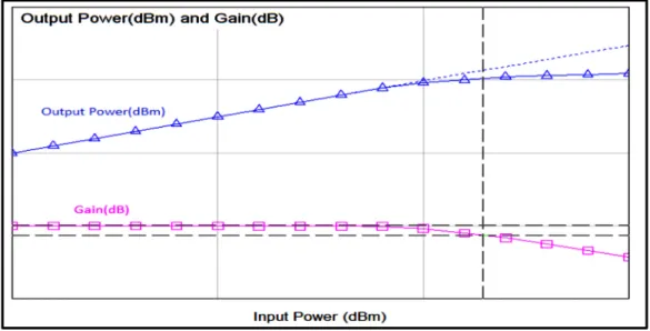
As shown in Equation (1.2), when the input power rises, the output power will constantly rise as a result. However, in realty, high input power causes the amplifier to saturate from nonlinear behaviour, resulting in gain compression, as depicted in Figure 1.2.
DC Power
Input Output
Power
9
Figure 1. 2 Input power, output power and power gain relation of a typical amplifier
The compression behaviour of a typical amplifier is represented by the two figures of merit Pout, -1 dB, which is the output power level that has deviated 1 dB from ideal linear behaviour, and Pin,-1dB, which is the corresponding input power level. Figure 2-3 illustrates these parameters, indicating that input power and output power measured at precisely 1 dB of compression can be formulated as:
Pout,dBm = (GdB) + Pin,dBm (1.3)
As mentioned above, saturation output power level is yet another parameter in a typical power amplifier. It indicates the maximum output power which may be removed. Figure 2.3 illustrates that rises in input power result in output power achieving the 1 dB compression point, after which further rises lead to output power saturation (i.e., maximum value).
We discussed previously how microwave PAs change DC power to microwave signal power, suffering loss from the process. A PA figure-of-merit, drain/collector efficiency, can be formulated as:
Where
is power efficiency. Pout is output power. Pdc is DC power.
To remove the majority of available power out of a PA, it must operate at high input power levels such that the levels of the DC power and output power are the same as the input power. This is accomplished through a power-added efficiency parameter, which considers the contribution of input power, as shown in Equation (1.5). Figure 1.3 depicts efficiency parameter, gain and output power all to be a function of input power.
=( − )/ dc (1.5) Where
is power add efficiency. Pout is the output power. Pin is the input power. Pdc is the DC power
Figure 1. 3 Power amplifier parameters Taken from Colantonin et al (2009)
11
1.2.1 Distortion Parameters
Because power amplifiers function in large signal sectors, the output signal from a PA becomes a changed version (i.e., distortion) of the input signal. This happens as a result of restrictions caused by the semiconductor. However, when a PA employs a 3rd order power
series approximation, the PA’s output voltage is formulated as a function of input voltage:
= + + (1.6) Where:
is power amplifier output voltage is the input voltage.
, , is amplifications factors.
Hence, if input signal presents as a single-tone excitation
= ×cos(2 ) (1.7)
The output voltage is
V = a + A × a + a A × COS(2πft) + a cos(2 ∗ 2πft) +
a COS(3 × 2πft) (1.8)
Equation (1.8) clearly indicates that when a single-tone signal affects a PA, the result at the output is the generation of DC, fundamental, 2nd and 3rd harmonic components. Therefore, by
applying Equation (1.8), input and harmonic power components are formulated as:
= (1.9)
P . = a × (1.11)
P . = a × (1.12)
From these formulations, we can see that the power of fundamental component becomes a function of the constants 1 / 3, along with input signal amplitude.
1.2.2 Harmonic Distortion
Equation (1.8) shows how PAs can create harmonic components as a result of single-tone excitation. Harmonic distortion can be defined as the amount of power in harmonic frequencies related to fundamental component power (Colantonio et all,2009). Given this definition, the nth harmonic distortion of HDnf can be formulated as:
HD ≜ (1.13)
Thus, in a 3rd power series approximation, the harmonic distortion in 2nd / 3rd harmonic
components is formulated by applying the harmonic powers from Equations (1.10) to (1.12): HD ≜ = × × = × (1.14) HD ≜ = × × = × (1.15)
Along with harmonic distortion in every harmonic component, we also obtain the Total Harmonic Distortion (THD):
THD = ∑ ,
13
1.2.3 Gain offset (AM/AM) and Phase Distortion (AM/PM)
Because the 3rd-order power series approximation from Equation (1.6) is a memoryless
operation, a few of the nonlinear effects are not visible. A PA’s input / output signals can be formulated as:
( ) = A( ) × cos(2 + ( )) (1.17)
( ) = G[A( )] × cos(2 + ( ) + [ ( )]) (1.18)
where:
G[A(t)] is Gain, nonlinear function of input signal amplitude.
[A( )] is Phase change inserted by PA, nonlinear function of input amplitude
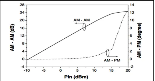
Nonlinear behaviour in gain is AM/AM, while nonlinear behaviour in phase change is AM/PM conversions. Moreover, amplitude’s nonlinear behaviour comes primarily from nonlinear transconductance, whereas phase’s nonlinear behaviour comes from nonlinear behaviour in internal capacitors and inductors from transistor models. Figure 1.4 depicts curves in AM/AM as well as AM/PM (Colantonio et all,2009).
Figure 1. 4 AM/AM and AM/PM characteristics of a typical PA Taken from Colantonin et al (2009)
However, it is well known that nonlinear input drive-dependent AM/AM and/or AM/PM behaviours are problematic in communications devices because they have a negative impact on the system’s constellation diagram. As well, AM/PM conversions occurring in phased array systems could negatively affect the antenna’s beam-forming capacity, leading to reduced performance.
1.2.4 Power Amplifier Classes
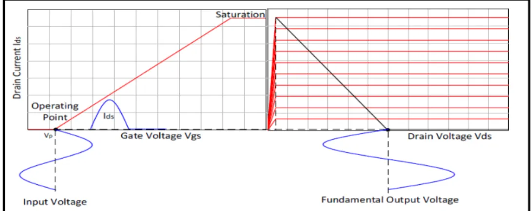
Power amplifiers (PAs) are classified as either linear or non-linear. In general, linear PAs can create output power that is directly proportional power being input without creating excessive harmonic power, whereas in non-linear PAs, input and output are not proportional, as the PAs function close to cut-off regions and create sizeable harmonics along with the main signal. Similarly, amplifiers can also fall into one of two classifications (classes), namely biasing or switching classes, (Colantonio et al, 2009). Biasing amplifiers (e.g., class A,B, AB and C amplifiers) are categorized as such due to their inherent quiescent point (bias point) and/or output Current Conduction Angle (CCA) θ. In this case, θ can be defined as: “the fraction of RF input drive signal where non-zero current is flowing through the device”, (Colantonio et al, 2009). In contrast, switching class amplifiers (e.g., Class E and Class F amplifiers) have a network configuration attached to an active element, though not at the bias level. Hence, switching transistors are switches that turn off and on in accordance with input drive signal , (Colantonio et al, 2009). It is worth noting that because Class E / F amplifiers can offer high power-added efficiency, they are attracting increasing interest from researchers and engineers alike. However, in our current study, we will deal almost exclusively with classes A, B, AB, E, inverse F (F-1) and F (the latter in greater detail).
1.2.4.1 Class A Power Amplifier
Class A amplifiers are linear and have a conduction angle of 360°, which indicates the transistor is turned on and able to conduct across a whole sinusoidal cycle. The majority of small-signal amplifiers fall into this designation due to their relative simplicity of design and
15
optimal linearity. However, the 360° conduction angle of Class A amplifiers gives them ultra-low efficiency, thus rendering them applicable mainly to low-power applications. Class A amplifier transfer characteristics, along with corresponding voltage / current waveforms, are illustrated in Figure 1.5.
Figure 1. 5 Input and output waveforms of class A power amplifiers
1.2.4.2 Class B Power Amplifier
Class B amplifiers’ bias level is lower than Class A’s and near the cut-off region. Unlike Class A, the transistor in Class B completes only half an input drive signal cycle, giving these amplifiers a CCA measuring approximately 180° and improved efficiency over Class A , (Colantonio et al, 2009). Class B amps typically show low-grade performance for linearity (due to excessive higher order harmonics), but this can be mitigated by employing dual transistors in a so-called push-pull setup. However, in this 2-transistor setup, both transistors can be OFF simultaneously, resulting in crossover distortion. Figure 1.6 illustrates Class B amplifiers’ transfer characteristics as well as corresponding voltage / current waveforms.
Figure 1. 6 Input and output waveforms of class B power amplifiers
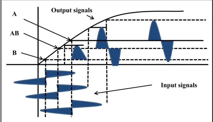
1.2.4.3 Class AB Power Amplifier
As their name implies, Class AB amplifiers function as a combined version of classes A and B amplifiers with regard to efficiency and linearity. Hence, the efficiency and bias point of Class AB amps is situated somewhere between classes A and B amps, as illustrated by Figure1.8. Furthermore, the crossover distortion of Class B is significantly less in Class AB push-pull amplifiers , (Colantonio et al, 2009), giving better linearity. Class AB’s transfer characteristics along with corresponding voltage/current waveforms are shown in Figure 1.7.
Ids
Vds
Input signals
Q
17
A comparison between the three classes is shown in Figure1.8. As can be seen, the Class A bias point can be found half-way between the saturation and cut-off region, and the channel shows as constantly ON. Furthermore, the input signal is followed by the output signal. Also shown in the figure is that the bias point for Class B is situated close to the deep cut-off region and provides a half-sine wave near the output, with even harmonics only , (Colantonio et al, 2009). Finally, the bias point for Class AB can be found situated midway between classes A and B, with the output signal following 50% the given input signal.
1.2.4.4 Class E Power Amplifier
Also labeled as the ‘switching class’, Class E amplifiers are easily identifiable by their network configuration to the input and output. Equipment in this class acts like a switch, going ON or OFF for duty cycles of approximately 50%. Class E’s employ reactive elements for their output network in order to increase efficiency through zero voltage switching (ZVS) as well as zero voltage derivative switching (ZVDS), the latter which is zero voltage with the
B
AB
A
Input signals
Output signals
switch ON. In ZVDS, no overlap exists between voltage / current waveforms, meaning there is zero loss from the switching , (Colantonio et al, 2009).
Figure 1.9 shows a transistor (depicted here as a switch symbol), with the Cp indicating a shunt capacitor that models the transistor intrinsic parasitic capacitance as well as the circuit capacitance. The aim is to ensure the amp’s appropriate proper switching behavior. The Ls and Cs create a series resonator that operates near the fundamental frequency and only passes this signal to the load. The capacitor Cp charges if the switch is ON. However, if the switch is OFF, Cs and Ls function in series together with R, forming a damped oscillating circuit. This enables the Cp to discharge at the resistive load R , (Colantonio et al, 2009).
Figure 1. 9 Circuit diagram for Class E amplifiers Taken from Rosu(2011)
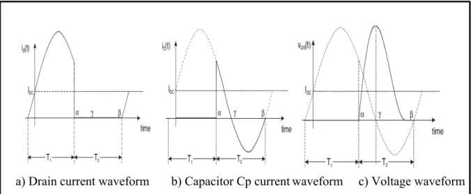
In Figure 1.10, we can see a depiction of the drain current waveform during ON (T1) and the capacitor current waveform during OFF (T2), as well as the drain voltage waveform during period T2. In Figure 1.11, we can see the voltage waveform during OFF and the current waveform during ON. It is worth noting that because there is zero overlap between the voltage and current waveforms, there is zero power consumption under RF functioning.
19
a) Drain current waveform b) Capacitor Cp current waveform c) Voltage waveform
Figure 1. 11 drain voltage and current waveforms of Class E Taken from Colantonio et al (2009)
1.2.4.5 Class F Power Amplifier
Class F amplifiers represent the successful ‘marriage’ of the best of classes B and E. To attain Class E ZVS and ZDVS, the efficiency and fundamental signal power are increased through the control of harmonic content and waveforms near the Class F drain , (Colantonio et al, 2009). Class F amps are biased with a quiescent point similar to Class B’s (a CCA of 180°). As mentioned previously, switching in the active equipment causes harmonics in the transistor. A negative feature in biasing-class amplifiers, harmonics are actually generated intentionally to increase Class F’s PAE. While, theoretically, Class F amplifiers can attain
Figure 1. 10 Drain current, capacitor current, and drain voltage waveforms of Class E Taken from Colantonio et al (2009)
perfect efficiency with no power consumption or harmonics power sent to the load, nearly an infinite number of harmonics have to be controlled, making this “perfection” unrealistic, (Schmelzer, 2007).
We would see the voltage waveform near the drain as a perfect square wave and the corresponding drain current waveform as a 180° out-of-phase half-sine wave, (Colantonio et al, 2009). Under such theoretically attainable situations, there would be complete elimination of the overlapping area between voltage and current waveforms, with zero power being consumed at the switching. Figure 1.12 illustrates this ideal (but currently unrealistic) Class F voltage and current waveforms giving 100% operational efficiency. Further underlying the theoretical base of this assumption, Equations (1.19) and (1.20) provide formulations for Class F current and voltage waveforms. In the formulations, Ø represents the phase differences in fundamental signal and harmonics, (Colantonio et al, 2009).
Although past research into Class F amplifiers has mostly looked into the output network, more recent inquiries point to the input network’s importance for efficiency improvement, especially the second harmonic input termination’s shaping of waveforms at the input and subsequent PA level. Experiments were conducted both with and without input wave-shaping network, showing that PA without it gave a maximum PAE of 60.31%, whereas PA with it (to control 2fo and 3fo) gave PAE of 88.97%. This represents nearly a 30% boost in PAE.
Figure 1. 12 Voltage waveform (blue) and current waveform (red)
Magnitude Current(A) Voltage(V)
21
V(t) = Vdd + V1 cos(wt + Ø1) + V2 cos(2wt + Ø2) + V3 cos(3wt + Ø3) + … (1.19)
I(t) = Idd + I1 cos(wt + Ø1) + I2 cos(2wt + Ø2) + I3 cos(3wt + Ø3) + … (1.20)
To achieve a truncated half-sine current waveform giving a perfect (theoretically idealized) efficiency rate, we applied a normalized Fourier Series Expansion closed-form equation for the coefficients, as shown in Equations (1.23) and (1.24) , (Colantonio et al, 2009). In the equations, n indicates harmonic order.
A = (1.21)
A = (1.22)
A , = ( ) (1.23)
A , = 0 (1.24)
Next, to achieve perfect square voltage waveform for perfect (theoretically idealized) operational efficiency, we applied normalized Fourier Series Expansion closed-form coefficient equations, as shown in Equations (1.27) and (1.28) , (Colantonio et al, 2009). In these equations, n indicates harmonic order.
B = (1.25)
B = (1.26)
B , = ( ) (1.28) As we can see from Equations (1.23) and (1.24), we first have to get rid of the odd harmonics in the current waveform near the drain if we are to form a truncated half-sine waveform featuring even harmonics only. Next, and as illustrated in Equations (1.27) and (1.28), we also have to get rid of the odd harmonics in the voltage waveform near the drain if we are to create a perfect square waveform that features even harmonics only , (Colantonio et al, 2009). Both of these steps have to be taken if we are to get rid of any overlapping area between voltage and current waveforms that have zero power consumption on active equipment.
In Figure1.13, we can see how the presence of harmonics impacts the shaping of voltage and current waveforms. On the right side, the voltage waveform’s top and bottom are flattened, while the transition slope steepens when additional even harmonics are included. On the left side, the current waveform’s negative swing is flattened, while transition time speeds up when additional odd harmonics are included. In reducing voltage and current signal transition time, the size of the signals’ overlapping area is decreased, and efficiency gets a boostTo
Figure 1. 13 Drain voltage (left) and current (right) waveforms at different numbers of harmonics
23
achieve a desired drain waveform, amplifier output networks need to have certain termination impedances for various harmonics. More specifically, for the harmonics needed to shape voltage waveforms, output networks have to present either an open or a high impedance near the transistor drain in order to prevent harmonic power from escaping. Unwanted harmonics can be dealt with by short / low impedance at the transistor drain to decrease harmonic power.
As can be seen in the figures below, inverse Class F (F-1) amplifier waveforms present as the inverse of Class F amplifiers, such that a Class F-1 amplifier shows a half-sine voltage waveform and square current waveform near the drain, as illustrated in Figure 1.14 “Maximum efficiency and output of Class-F power amplifiers. Furthermore, Equations (2.29) and (2.30) calculate the output impedance for classes F and F-1 amplifiers.
Output impedances for Class F: Z2n = 0 , Z2n+1 = ∞ … (1.29) Output impedances for Class F-1: Z2n = ∞ , Z2n+1 = 0 …. (1.30) where n = harmonic order
As mentioned above, perfect efficiency can be attained theoretically, but at the expense of simplicity (i.e., the matching networks will grow impossibly complex with the need to control a near-infinitive number of harmonics). This situation is neither practical nor
Figure 1. 14 Invers Class F voltage and current waveforms at infinite number of harmonics
desirable. In simplified format, Figure 1.15 illustrates a schematic of the classes F and inverse Class F amplifiers’ output network. Also of note is that the high frequency signal has the tendency to flow into the source channel and short to the ground due to drain-source parasitic capacitance Cp of the transistor. This is shown in Figure 1.15, (Colantonio et al, 2009). The indication here is that higher order harmonics make reduced contributions either to waveform shapes or PAE. In fact, the transistor parasitic capacitance represents one of the key characteristics restricting the upper bound operating frequencies of transistors such that a small number (rather than an infinite number) of harmonics can be controlled. The filter block essentially operates like a harmonic trap whose purpose is to stop the delivery of harmonic power to the load. This makes it part of the fundamental signal’s impedance-matching network which can be utilized for form a desired waveform near the drain.
Figure 1. 15 The classes F and inverse Class F amplifiers
Class F topology can be categorized according to the highest order of harmonic that is under control, (Colantonio et al, 2009). So, for instance, a topology is referred to as a third harmonic peaking or third harmonic injection only if there is control present up to the third harmonic. Similarly, a topology is referred to as fifth harmonic peaking/injection only if there is control present up to the fifth harmonic.
25
Figure 1.16 illustrates a third harmonic peaking configuration in Class F amplifiers. As can be seen, the L3||C3 parallel resonator operates at the third harmonic frequency. This means that it is open to third harmonic signals but rejects any other frequency as a short circuit. Furthermore, the shunt parallel L1||C1 resonator functions at the fundamental frequency such that it shifts the fundamental frequency signal onto the load but shorts harmonics to the ground, resulting in zero harmonic power in the load. It is worth mentioning that output voltage and current waveforms show as being entirely sinusoidal as well as in phase due to the application of a 50Ω resistive load.
In most published research papers (Schmelzer,2007) (Raab,2001), the third harmonic peaking topology is practically applied in order to keep the network from being too complex while providing a robust performance. Normalized harmonic content up to third harmonic and the composition of voltage/current waveforms for third harmonic peaking is shown in
Figure 1. 16 3rd Harmonic peaking configuration using lumped elements
Figure 1.17. With proper magnitude of third harmonic voltage signal, a flattened top and bottom of the voltage waveform can be created
Figure 1. 17 Class F drain voltage and current waveform of 3rd harmonic peaking configuration blue – 1st harmonic / red – 3rd harmonic cyan – 2nd harmonic/green
Figure 1.18 below shows a more advanced Class F configuration, controlling all harmonics using lumped and distributed elements. As described before, L1||C1 parallel resonator provides a short to all harmonics at point B. With a quarter-wavelength transmission line (λ/4 transformer) at f0 placed between the shunt resonator and the drain, all odd harmonics will have 180° phase shift and all even harmonics phase will stay unchanged at point A. However, this would only be true in theory. In practice, a fixed λ/4 transformer at the fundamental frequency cannot be used for an infinite number of harmonics. As the frequency increases, the line becomes more inductive to the signal and causes imperfect transformation between an open and a short. Moreover, L1||C1 resonator in parallel with the load is assumed to have an infinitely high-quality factor, which is hard to achieve in real implementation. Quality factor for parallel resonators can be calculated according to kind of transistor. It requires a large capacitance C to inductance L ratio or large value of R in order for a high Q factor.
27
Figure 1. 18 Example of 3rd Harmonic peaking configuration
1.2.5 Quality Factor For RCL
There are 2 ways to implement a Class F PA. One way is to use lumped elements and the other way is to use distributed elements. This project will use distributed elements. Lumped elements are more suitable than distributed elements for low frequency applications because devices using lumped elements are smaller in size for such applications. However, lumped-element PAs are hard to design as the operating frequency gets higher because of the difficulty in finding small inductors in pH range value. Because of the tiny inductance required by the high Q resonator at high frequency, it makes the lump-element design impractical. Moreover, it is difficult to find ideal components without knowing the uncontrolled parasitic model of elements as the frequency increases. Therefore, lumped elements with low percentage tolerance such as 2% must be chosen and experimentally characterized before the usage. A few percent of variation in lumped element values will have a great impact on the system performance. Moreover, it is difficult to obtain inductors.
= (1.31)
1.3 Power Amplifier Circuit Blocks
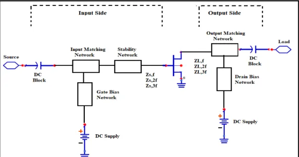
To get a deeper understanding of a class F power amplifier’s internal dynamics, designers can break down a device into relevant circuit blocks. Figure 1.19 illustrates how a PA can be divided into blocks. Such a breakdown can also be applied as the topology in high-frequency designs. The present thesis work employs this specific topology for its PA design.
In a typical power amplifier, an output matching network changes the load impedance to optimal impedance given in the transistor and drain bias network in order to use drain bias voltage. The output matching network is then integrated with the drain bias network.
However, in the present study, the two networks are viewed as separate circuit blocks in order to better relay how each one works.
Along with an input matching network and a gate bias network, the input side in a power amplifier features a stability network. The design of the stability network must be such that it can handle the PA’s stability issues. As well, DC block capacitors are positioned on all sides of the amplifier. The purpose of these capacitors is to block any DC component in the incoming and outgoing signals, and thus to permit the propagation of RF signals only.
29
1.3.1 Stability Network
A very crucial aspect of power amplifiers is that they not oscillate. However, because of feedback mechanisms in transistors, output signals could potentially be rerouted at the input side; if this occurs, and the input and feedback signals share some of the same phases, this could lead to oscillations. While the process may be done on purpose for oscillator circuits, it is undesirable in amplifiers because it negatively impacts their performance and also can be dangerous. So, following the decision regarding operational class, the next step is performing a stability analysis for the transistor, as well as designing a stability network, if one is required.
If circuits lack the necessary stability for the application, there is the potential for unlimited increase in signal. This situation puts the active devices into the mode of large signal operation and/or saturation. To avoid this unwanted scenario, power amplifiers need to be stable across all frequencies as well as all source-load impedances. Oscillations could cause any one or more of the following problems (Gilmore et all,2003):
• Unusually noisy circuits,
• Damage to the device being used, caused by undesirable large signal operation, • Saturation of the active device, resulting in the circuit design becoming invalid.
We can use a few different approaches to find out whether or not a transistor is potentially unstable. One of the simplest approaches is the μ-factor, in which the designer only has to consider a single parameter to see if the device is stable. This parameter is:
=| ∆ |∗| || ∗ | (1.32)
where ∆= S11 ∗ S22 − S21 ∗ S21
The designer needs to take the μ-factor into consideration for the zero frequency up to the high frequencies for the applicable band, adding to the design a stability network if one is required. In the present work, the μ-factor has been applied to the design process in order to
assess any stability issues occurring at circuit level. As the μ increases, there is also a reduction in maximum available gain (MAG) from the applicable active devices. So, for the band of interest, the μ-factor should be sufficiently big to give a stable operation while at the same time being sufficiently small to get high gain. Chapter 4 discusses a few simulations involving the μ-factor relation to MAG.
Stability networks are a prerequisite for circuits, if the aim is to have unconditional stability across all frequencies and impedances involving the transistor. Figure 1.20 illustrates two stability network topologies. In this study, the topology in Figure 1.20.a is used mainly because it is easy to implement with microstrip circuits. The RC network’s equivalent series impedance is expressed as:
Z = ∗ ∗ − j ∗ ∗∗ ∗ (1.33)
The resistance from the equivalent impedance boosts the loss amount at the power amplifier’s input side. Therefore, because transistors generally exhibit higher gain in low frequencies, and also because the available gain goes down when the frequency goes up, the transistor requires high resistance for low frequencies but lower resistance when the frequency goes up to ensure stability. Equation (1.33) shows how resistance goes down when frequency goes up, indicating that the capacitor’s reactance is becoming short. Power amplifiers benefit from this scenario because of the available gain-frequency relationship, so choosing the right R and C results in a network that has unconditional stability.
However, in actual applications, higher frequencies means that circuit elements have to be comparable to wavelength and that the circuit elements as act as distributed elements. In this work, the R-C network is being designed with distributed resistance and capacitance that feature parasitic components (e.g., additional shunt capacitances and inductances) on the actual elements. These inductances and actual capacitance C could potentially resonate and create open circuits on a frequency band, leading to only the series resistance being effective. As a result, there could be undesirable high loss. To prevent this situation, designers should
31
take the time to model the circuit elements in order to gauge the impacts of the parasitic components as well as the actual high frequency
Figure 1. 20 Stability network topologies
1.3.2 Matching Networks
Input and output matching networks work together to create optimal impedances. These are derived from the active devices load pull data at the gate and drain. Another important feature in these networks is low loss matching elements, which prevent power loss during output/input stages. However, because the large size of lumped elements makes them impractical for microwave frequencies, distributed elements like short or open stubs and series transmission lines can be employed instead for matching elements.
Complex impedances can be matched by employing single or double stub lossless matching networks. These are then realized by employing microstrip series lines or stubs. Because one part of a single stub matching network is unable to accomplish wideband matching, multi-section networks have to be utilized for impedance matching in wide bandwidths. Figure 1.21 illustrates an open single stub matching network, while Equation (1.34) expresses the input impedance.
= − ∗ + ∗ ∗ ∗
∗ ∗ (1.34)
Figure 1. 21 Single, open stub matching network
An additional issue in the matching strategies mentioned above is how the approaches are based on having continual input / output impedances across frequencies, but a power amplifier’s optimal impedance gets altered in the interested frequency band. So, for wideband matching, the impedance transformation has to be monitored in the matching network and for the entire frequency band. One typical method involves using quarter wavelength transformers as well as low pass matching networks simultaneously in order to realize the necessary impedance matching for interested frequency bands.
On the other hand, if the requirement is for high RF output power, wide gate periphery devices are preferable as they significantly reduce the transistor’s load and source impedances. This effect will be demonstrated later in Chapter 4 of the present work. The transistor employed as this thesis study’s active device displays an optimal load impedance (real part) of 2 ohms. So, in matching 2 ohms and 50 ohms, the output matching network has 1:25 as an impedance transformation ratio but matching this in wide bandwidths is difficult.
1.3.3 Bias Network
When bias network elements cannot be applied in matching elements, this means that the bias network input impedance is extremely high and open circuit. In low-frequency
33
amplifiers, we can use bias networks with RF chokes. Bias networks can be developed with λ/4 transmission lines for microwave frequencies.
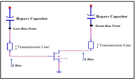
Figure 1.22 shows drain bias and lumped element gate networks. As can be seen, the electrical length separating the RF choke from the decoupling capacitor has to be relatively short so as not to alter the RF short impedance. For this reason, PA designers can use the Smith chart for their RF bias network design in order to locate the Z_bias impedance.
Figure 1. 22 A typical lumped element gate and drain bias networks
Figure 1.23 depicts a bias network which has been synthesized utilizing λ/4 transmission lines along with decoupling capacitors for gate/drain bias point short circuiting (ultra-low impedance). Theoretically, as reduced impedance behaviour in a capacitor comes from increasing the frequency, we assume that the capacitor’s bias points have quite low impedance values (that is, near short-circuit status on the Smith chart). But theory is not practice, so in reality, capacitors tend to exhibit complex electrical modeling, meaning that they exhibit resonance frequencies that lower the frequency spectrum’s usable range.
Figure 1. 23 A typical distributed bias network with short circuit capacitor
Figure 1.24 illustrates a wideband distributed element bias network. As can be seen from the figure, the λ/4 microstrip butterfly stub serves as the wideband short circuit for the biasing point, while the λ/4 transmission line changes the short circuit into an open circuit. Moreover, because the microstrip butterfly stub is a short circuit, we no longer require a close bypass capacitor. To deal with any abrupt alterations that negatively impact performance, we can use a decoupling capacitor in order to decouple circuit and supply.
Figure 1. 24 A typical distributed bias network with butterfly stub
Butterfly stub Butterfly stub
Transmission Transmission
35
1.4 Literature review:
Within wireless communications systems, power amplifier blocks typically use up the majority of the available power. This situation will only get worse, as the latest versions of technology require more and more data transmission capability at the same time as they demand as little spectrum usage as possible. The key to this dilemma of creating high data transmission abilities with low spectrum usage is to optimize power efficiency through reductions in off-chip components used in the radio frequency transmission systems. This would be particularly relevant in mobile wireless applications, which demand the smallest possible sizing. Extensive research has been performed on these issues thus far. Below is a summary of the most relevant and promising results in the literature.
Kuroda et al. (2012) looked at designing and fabricating a class F amplifier by employing AlGaN/GaN HEMT at 5.7 GHz. However, when operating at 5.7 GHz, the parasitic effects (e.g., output capacitance in bounding wires) need to be eliminated, which is accomplished through adjusting the load circuit. The researchers applied nonlinear analysis and exact large-signal model parameters from computer simulations to design their class F amplifier and used harmonic impedance tuning to improve their efficiency rates. Kuroda et al.’s (2012) amplifier, which incorporated a low-loss resin microstrip substrate into the design, maximized drain efficiency up to 77.1% and power-added efficiency up to 68.7% when operating in the 5.69 GHz range. It was critical to reduce losses in the parasitic resistances, as these can lower efficiency levels (Kuroda et al., 2012).
Ahmed (2016) pursued a class F PA design strategy that used Gigahertz frequencies. Class F can be applied in wire application PAs of any frequency that require high output power, good gain, and high efficiency. Several different harmonic terminations using design approaches like load network with lumped LC elements are potential contributors to enhancing efficiency in class F PAs. Thus far, the best PAE recorded in the literature is 82.9%, which falls far short of the potential and ideal 100% efficiency rate. Ahmed (2016) suggested adopting a novel method that incorporates wireless RF applications in order to attain higher efficiency in class F PAs.
In Hayati (2015), a novel structure was in fact realized for efficiency and high-frequency class F Pas. The researcher employed ATF-34143 pHEMT transistors which were loaded optimally for harmonic and fundamental frequencies. Hayati’s (2015) results show that a highly efficiency class F PA mode was attainable for 2.4 GHz, with a PAE at 80% and 23.6 dBm output power. In this design, the size reduction was achieved by paring back the sizes of the output matching circuit and harmonic control circuit (Hayati, 2015).
Gaw et al. (2005) developed a class F amplifier which featured high PAE, using pHEMT technology. The design method was simulation-based and employed a load-pull/source-pull strategy. Results for 2 GHz showed excellent agreement with the simulation and underscored the importance of the second harmonic input tuning. Also in Gaw et al. (2005), there was a comparison of cases both experimentally and theoretically, showing worst and best and case terminations measuring, respectively, 42% and 76% saturated PAE. This design strategy could be applied for optimizing the intermodulation distortion and additional output power of a range of Pas (Gaw et al., 2005).
Shang et al. (2016) explored the development of a novel high-efficiency K-band MMIC medium-power PA. The design incorporated multi-harmonic matching through the application of GaAs pHEMT process technology and functioned at 26GHz frequency using 2GHz bandwidth. The researchers attained an output power of 20 dBm 1 dB compression-point with an efficiency of 40%. For evaluating thermal characteristics, the researchers also proposed the design of a novel thermal reliability analysis strategy which could be based on ICEPAK (Shang et al., 2016).
As shown above, few techniques are implemented at 5.7 GHz. Furthermore, few of these have been fabricated using the LTCC. The proposed research is focused on a class F power amplifier design at 5.7 GHz using GaN technology. In addition, a novel thermal reliability analysis method is proposed also to evaluate PA thermal characteristic
CHAPTER 2
ELECTRICAL DESIGN OF CLASS F POWER AMPLIFIER 2.1 Introduction
Chapters 1 presented the main ideas and parameters to consider when designing a power amplifier. Chapter 2 will present the basic requirements for designing and building a power amplifier prototype. As will be seen, designing a PA requires several steps, each one of which can have an impact – for good or for bad – on the PA’s performance capabilities. After the PA is constructed, small- and large-signal simulations will be carried out to compare the performance of this PA with those in the literature. As well, circuit topology and a drain voltage pulsing method is presented.
In PA design, the process begins by defining the requirements and specifications. The process is completed when the newly designed PA has been validated, meaning that it has met all or most of the stated requirements and specifications. The next sections provide a detailed outline of the design process.
2.2 Requirements
Performance requirements for PA design usually include factors like bandwidth, efficiency, output power and gain, as well as specifications on linearity parameters, electrical performance, and mechanical dimensions. Additional factors and specifications could involve temperature range, which would mean that thermal precautions would have to be included in the design.
The PA should include the following features. In fact, these requirements lay the groundwork for subsequent design decisions.
Table 2.1 PA Requirements
Parameter Requirement Operating Frequency 5.7 Ghz
Input Power 25 dBm
Output Power 36 dBm
PAE As high as we can
Small Signal Gain 17 dB
2.3 Device selection
The design process has several steps. As a first step, deciding which active device (here, the transistor) to use is very important. The transistor must not only have suitable efficiency and output power, but also the right gain, linearity requirements, and reliability. Table 2.2 compares a few semiconductor materials and their parameters, (Runton et al, 2013). So, for instance, if we need high power density, the best option might be GaN devices, but they are quite expensive. On the other hand, if cost is more important than power, a GaAs device would be ideal. Another consideration is the transistor’s upper limits for operation frequency. These need to be checked to see if the operation band suits the project center frequency and bandwidth.
Table 2.2 Some properties of semiconductor materials
Property Si GaAs GaN SiC InP
Electron Mobility ( ) 1500 8500 1000 900 5400
Hole Mobility ( ) 450 400 350 120 200
Saturated Drift Velocity (10 / ) 1 2 1,8 0,80 2
Thermal Conductivity (W/cm.C) 1,40 0,45 1,7 4,90 0,68
Dielectric Constant 11,90 12,90 14 10 8