Adaptable Power Conversion for Grid and Microgrid
Applications
by
Wardah Inam
B.S. Electronics Engineering, GIK Institute (2010)
S.M. EECS, Massachusetts Institute of Technology (2013)
Submitted to the Department of Electrical Engineering and Computer
Science
in partial fulfillment of the requirements for the degree of
Doctor of Philosophy
at the
MASSACHUSETTS INSTITUTE OF TECHNOLOGY
June 2016
© Massachusetts Institute of Technology 2016. All rights reserved.
Author . . . .
Department of Electrical Engineering and Computer Science
May 20, 2016
Certified by. . . .
David J. Perreault
Professor, Department of Electrical Engineering and Computer Science
Thesis Supervisor
Certified by. . . .
Khurram K. Afridi
Assistant Professor, University of Colorado Boulder
Thesis Supervisor
Accepted by . . . .
Leslie A. Kolodzeijski
Chair, Committee on Graduate Students
Adaptable Power Conversion for Grid and Microgrid
Applications
by
Wardah Inam
Submitted to the Department of Electrical Engineering and Computer Science on May 20, 2016, in partial fulfillment of the
requirements for the degree of Doctor of Philosophy
Abstract
Power electronics convert and control power and are an essential part of many elec-tronic devices and systems. Increasingly, power converters need to operate over widely varying operating conditions (voltage, current and power level), which can degrade their performance. In many applications, power converters are also being intercon-nected to form power systems. This is challenging as the converters may have to operate in various configurations. In order to ensure best performance, power con-verters and systems need to adapt to the operating conditions by adjusting topology, component values or control characteristics. In this thesis, two applications are con-sidered: universal input power supplies and off-grid electrification.
More than 3 billion power supplies were sold worldwide in 2014 [1], with effi-ciencies ranging from 50-90% [2], which results in significant energy loss. A major portion of these are universal input power supplies (designed to operate at AC line voltages found globally). In this thesis, a control technique, Variable Frequency Mul-tiplier (VFX), is developed which compresses the effective operating range required of a resonant converter by switching the inverter and/or rectifier operation between processing energy at a fundamental frequency and one or more harmonic frequencies. This technique was applied to the inverter stage of a stacked-bridge LLC converter for a universal input power supply. An efficiency of 94.9% to 96.6% was achieved for a 50 W converter operating across the entire (4:1) input voltage range.
Even though centralized grid infrastructure is widespread, access to electricity is still limited in many parts of the developing world. More than 1.2 billion people globally do not have access to electricity [3]. In this thesis, an ad hoc modular microgrid architecture is developed and field-tested. Contrary to how conventional power systems are designed, these microgrids do not require pre-planning and can operate in any network configuration. Smart power management units have been designed to arbitrarily connect power sources and loads, forming an autonomous microgrid. Accurate power sharing of multiple power sources is demonstrated. A methodology to attain the lowest system cost by designing power converters that reduce lifetime energy loss has also been developed. This enables affordable and
reliable electricity to be provided in off-grid areas.
Improvements in these applications will have a significant impact on power uti-lization from the existing grid infrastructure, and will help define the future of power utilization where this infrastructure does not exist. Moreover, the techniques and designs developed, in this thesis, for adaptable and efficient operation of power con-verters and systems can be easily extended to other applications.
Thesis Supervisor: David J. Perreault
Title: Professor, Department of Electrical Engineering and Computer Science Thesis Supervisor: Khurram K. Afridi
Acknowledgments
First and mostly importantly, I want to thank Professor David Perreault, my thesis advisor, with whom I was fortunate to work for the many years of graduate school. He taught me most of what I know about power electronics, and how to systematically approach difficult problems. He was extremely supportive of whatever project I have undertaken. He not only advised me to always have very high standards for my work, but also helped me grow as a researcher, and as a person.
My thesis co-advisor; Professor Khurram Afridi, for his invaluable guidance, en-couragement and faith in me. He was crucial in shaping the direction of this research, and meticulously went through all its details. I was very fortunate to have the chance to work with and to learn from him. My thesis committee member; Professor Rajeev Ram, one of the most knowledgeable people I know. I learned a lot about work and life from him. He also inspired me to think big. The deputy director of MIT Energy Initiative; Rob Stoner, who adivsed me on how to practically apply my research to have a larger impact, and tried to remove all barriers that came in the way.
I would also like to thank the undergraduate researchers who were crucial in this project; Erik Johnson, Ahmet Musaboyoglu, who joined me early on to build the first converters and to conduct field trials. Julia Belk and Thipok Rak-amnouykit who joined me later in advancing the work to a point where we have a finished product that we are very proud of. Members of my research group: Minjie Chen, Samantha Gunther, Juan Santiago, Alex Jurkov, Seungbum, Alex Hanson, Yiou He, Wei Li for informative discussions and many laughs that we shared together. My friends in LEES: Richard Zhang, Kendall Nowicin, David Jenicek, Jorge Elizondo, Shahriar Khushrushahi, for a great time at MIT.
Last, but not the least, I would like to thank my family for their unconditional love and support. I am very grateful to have them in my life. Especially my husband, Ahmed Malik. Words cannot express my gratitude for everything he has done to make this possible and to make this journey immensely enjoyable.
Contents
1 Introduction 21
1.1 Motivation . . . 22
1.1.1 Efficient universal input power supplies . . . 22
1.1.2 Ad hoc microgrids for off-grid electrification . . . 22
1.2 Background and Thesis Contribution . . . 23
1.2.1 Efficient universal input power supplies . . . 23
1.2.2 Ad hoc microgrids for off-grid electrification . . . 25
1.3 Thesis Organization . . . 26
2 Variable Frequency Multiplier Technique 27 2.1 Technique Applied to an Inverter . . . 28
2.2 Technique Applied to a Synchronous Rectifier . . . 33
3 VFX Technique Applied to the Dc-Dc Converter of a Power Supply 37 3.1 Experimental Prototype and Results . . . 41
3.2 Conclusion . . . 46
4 A Case for Innovation in Electricity Access 47 4.1 Understanding Energy Access . . . 47
4.2 Different Approaches for Electricity Access . . . 48
4.3 Providing Affordable Electricity . . . 50
4.3.1 Drivers of cost of electricity . . . 50
4.4 Impact of Electricity Access . . . 52
4.4.1 Social and economic impact . . . 52
4.4.2 Environmental impact . . . 54
5 Ad Hoc Microgrids for Off-grid Electrification 55 5.1 Definition . . . 55
5.2 Type of Distribution . . . 56
5.2.1 Type of power generation . . . 56
5.2.2 Types of loads available . . . 57
5.2.3 Size of the grid . . . 57
5.2.4 Safety . . . 57
5.2.5 Stability . . . 59
5.2.6 DC distribution chosen . . . 59
5.3 Overview of the Micorgrid . . . 59
5.4 Ensuring Arbitrary Interconnection . . . 61
5.5 Control of Distributed Power Sources . . . 63
5.6 Design Methodology . . . 65
5.6.1 Power rating . . . 65
5.6.2 Voltages of operation . . . 66
5.6.3 Motivation for modularity . . . 68
5.7 Software Overview . . . 69
5.7.1 Scheduling . . . 69
5.7.2 Real-time dispatch . . . 70
5.8 Conclusion . . . 70
6 Designing Low-cost Source and Load Converters 73 6.1 Source Converter . . . 73
6.1.1 Selection of topology to reduce cost . . . 74
6.1.2 Designing the power stage of the source converter . . . 75
6.1.3 Cost of the converter . . . 77
6.1.5 Experimental results . . . 81
6.2 Load Converter . . . 82
6.2.1 Designing with safety consideration . . . 83
6.2.2 Topologies considered . . . 86
6.2.3 Design of the 12 V power stage . . . 87
6.2.4 5 V output post regulating converter . . . 96
6.2.5 Converter for current-regulated output . . . 98
6.2.6 Experimental prototype and results . . . 99
6.3 Evaluating Capacitive Isolation for Load Converter . . . 99
6.3.1 Safety capacitors . . . 101
6.3.2 Design of a capacitively isolated load converter . . . 104
6.3.3 Experimental results of the capacitively isolated load converter 107 6.4 Conclusion . . . 113
7 Designing Converters to Reduce System Cost 115 7.1 Converters Evaluated . . . 117
7.1.1 Flyback converter . . . 117
7.1.2 Multi-output resonant converter . . . 118
7.2 Determining the Weighted Efficiency of a Converter Resulting in Min-imum Energy Loss . . . 121
7.2.1 Annual load profile . . . 121
7.2.2 Weighted efficiency . . . 122
7.3 Determining the Cost of Efficiency of the Power Converters . . . 125
7.4 Conclusion . . . 130
8 Stability and Control of Ad Hoc Dc Microgrids 131 8.1 Microgrid Architecture and Models . . . 133
8.1.1 Hierarchically-controlled sources . . . 133
8.1.2 Loads . . . 134
8.1.3 Interconnecting lines . . . 134
8.1.5 Mathematical representation . . . 136
8.2 Existence and Feasibility of Equilibrium . . . 137
8.2.1 “Worst-case” network configuration . . . 138
8.2.2 Existence of equilibrium . . . 138
8.2.3 Feasibility of equilibrium . . . 139
8.3 Small-signal Stability . . . 140
8.3.1 Simple network . . . 141
8.3.2 General formulation . . . 141
8.3.3 Small signal stability: condition 1 of 2 . . . 142
8.3.4 Small signal stability: condition 2 of 2 . . . 143
8.4 Microgrid Control . . . 143
8.5 Experimental Validation . . . 146
8.5.1 Designing a sample network . . . 146
8.5.2 Experimental results . . . 148
8.6 Conclusion . . . 150
9 Conclusion 151 9.1 Contribution . . . 151
9.1.1 Efficient universal input power supplies . . . 151
9.1.2 Ad hoc microgrids for off-grid electricity access . . . 152
9.2 Recommendations for Future Research . . . 153
9.2.1 Efficient universal input power supplies . . . 153
9.2.2 Ad hoc microgrids for off-grid electricity access . . . 153 A Schematic, PCB Layout, Components Used and Code for VFX
Con-verter 155
B Design of Low-cost Converters: Schematic, PCB Layout,
Compo-nents Used and Code for Source and Load Converter 171
C Design of Converters to Reduce System Cost: Schematic, PCB Lay-out and Components of Resonant Converters, and System Level
Simulation Code 195
List of Figures
2-1 Stacked bridge inverter with input voltage 𝑉𝑖𝑛 and output voltage 𝑣𝑖𝑛𝑣. 28
2-2 Stacked bridge inverter with input voltage 𝑉𝑖𝑛 and output voltage 𝑣𝑖𝑛𝑣
in mode 1. . . 29
2-3 Output voltages of the two inverters 𝑣𝑖𝑛𝑣1 and 𝑣𝑖𝑛𝑣2 and the resulting inverter voltage 𝑣𝑖𝑛𝑣 in Mode 1. . . 29
2-4 Stacked bridge inverter with input voltage 𝑉𝑖𝑛 and output voltage 𝑣𝑖𝑛𝑣 in mode 2. . . 30
2-5 Output voltages of the two inverters 𝑣𝑖𝑛𝑣1 and 𝑣𝑖𝑛𝑣2 and the resultant inverter voltage 𝑣𝑖𝑛𝑣 in Mode 2. . . 31
2-6 Square pulse train output (𝑣𝑖𝑛𝑣1) with duty cycle 𝐷1 and time period T. 31 2-7 Normalized amplitude of the first four harmonics of a rectangular wave with duty ratio D. . . 31
2-8 Full bridge synchronous rectifier with a resistive output load. . . 33
2-9 Voltage waveforms at the rectifier input during mode 1. . . 34
2-10 Voltage waveforms at the rectifier input during mode 2. . . 35
3-1 Schematic of the LLC converter with a stacked bridge inverter incor-porating the VFX technique. . . 38
3-2 Fundamental harmonic model of the LLC converter. . . 39
3-3 Voltage gain of (a) the transformation stage and (b) converter, using FHA. . . 42 3-4 Picture of the (a) top side and (b) bottom side of the prototype board. 43
3-5 Current and voltage waveforms of the converter at 50 W when operated in mode 1, fundamental mode, and in mode 2, VFX mode. (1-Blue)
Gate voltage of switch 𝑆4, (2-Turquoise) drain-source voltage of switch
𝑆4, and (4-Green) current output of lower half-bridge that is flowing
into the transformer primary. . . 43
3-6 Efficiency of the converter (a) with variation in input voltage with fixed output voltage and 50 W output power operating in mode 1 and 2, and (b) with variation in output power with 170 V input voltage and fixed
output voltage operating in mode 1. . . 44
5-1 Aribitrary interconnecion of Power Management Units (PMUs)
form-ing an adhoc microgird. . . 55
5-2 The Power Management Units (PMUs) can connect power generating sources and loads to form an ad hoc microgrid. A residential microgrid
is depicted. . . 60
5-3 Detailed overview of the microgrid with connected PMUs. Each PMU
comprises of power conversion, control and communication modules. . 62
5-4 Two sources with output voltages 𝑣1 and 𝑣2 connected to a load 𝑅𝐿
with resistive lines 𝑅1 and 𝑅2. . . 64
5-5 PMUs to interface sources and loads to the grid network. . . 66
5-6 Power loss in distribution and wire cost with 25 W transferred at 24
V with 14 AWG wire costing $0.0578 per meter. . . 68
5-7 Overview of scheduling and dispatch in the grid. . . 71
6-1 Schematic of the source converter implemented using synchronous boost
topology. . . 77
6-2 Prototype board of the source converter . . . 77
6-3 Cost of 250 W bidirectional boost converter. Costs are based on
pub-lished distributor costs at 10,000 component pricing. . . 78
6-4 Average current control converter model . . . 79
6-6 Bode plot of 𝐺𝑣𝑖(𝑠) and 𝑇𝑣. . . 80
6-7 Bode plot of 𝑇 (𝑠). . . 81
6-8 Efficiency of boost converter from 2.5 W to 250 W for 12 V input and
24 V output. . . 81
6-9 Power can be transferred using spare pair of wires on ethernet cables.
Image from: Ethernet Protection Guide [4]. . . 84
6-10 Schematic of the load converter with a flyback main power stage. . . 87
6-11 Transfer function (𝐻𝑓 𝑙𝑦𝑏𝑎𝑐𝑘(𝑠)) of the flyback converter with and
with-out compensation. . . 94
6-12 Second order feedback using a (model) optocoupler and a TL431 shunt
regulator. This technique is described in [5]. . . 95
6-13 Converter System. . . 95
6-14 Model of the system for designing the EMI filter to not change the control-to-output dynamics of the converter and/or have input filter oscillations owing to the negative-input resistance effect of the
closed-loop converter. . . 97
6-15 Middlebrook’s impedance design criteria with input impedance of the
converter and output impedance of the filter. . . 97
6-16 Converter transfer function with and without the EMI filter. . . 98
6-17 Measured efficiency vs output power of the flyback load converter. . . 100 6-18 Prototype board of the load converter implemented using flyback
topol-ogy. . . 101 6-19 Cost of 25 W isolated flyback converter, with 10,000 unit pricing at
available distributor prices. . . 101 6-20 Capacitively isolated series resonant converter. . . 104 6-21 Fundamental harmonic approximation of the series resonant converter. 106 6-22 Efficiency of the capacitively isolated converter with respect to the
6-23 Efficiency of the capacitively isolated converter with respect to the chosen resonant capacitor with varying component 𝑄 of the inductor
plotted for 𝑓𝑠𝑤 = 1.5 MHz. . . 108
6-24 Picture of the (a) top side and (b) bottom side of the prototype capac-itively isolated board. . . 109
6-25 Cost of capacitively isolated load converter, based on 10,000 units at published distributor costs. . . 110
6-26 Switching waveforms of the Inductor current and output voltage of the inverter at full load. . . 111
6-27 Switching waveforms of the Inductor current, output voltage of the inverter and gate signal of bottom switch at 2.5 W of outptut power. 111 6-28 Estimated loss break-down of the capacitively isolated converter. . . . 112
6-29 Frequency control and assymetrical duty cycle control used to control the converter as load varies. . . 112
6-30 Experimental efficiency of the converter as load varies from 2.5 W to 25 W with 28 V input voltage 12 V output voltage. . . 113
7-1 Flyback converter. . . 116
7-2 Multi-output resonant converter with litz wire transformer. . . 117
7-3 Multi-output resonant converter with PCB transformer. . . 117
7-4 Efficiency vs output power of the three converters built. . . 118
7-5 Percentage of energy processed by the load converter including varia-tion in each load’s power consumpvaria-tion. . . 123
7-6 Percentage of energy processed by the load converter, assuming no variation in each load’s power consumption. . . 124
7-7 Cost of the 12 V power stage of each of the three converters. . . 125
7-8 Determining the cost of the system with each power converter. . . 126
7-9 A six power management unit system depicting the losses incurred. . 127
7-10 Cost breakdown of the system with five Flyback load converters and one source converter. . . 129
8-1 Source model with successive levels of hierarchical control. 𝑣𝑘 is the
converter output voltage. The model with primary control is used for stability analysis in Sections 8.2 and 8.3; secondary control is discussed
in Sections 8.4 and 8.5. . . 132
8-2 Load model. (a) Constant power load with input capacitance, (b) Linearized model used for small signal analysis: 𝑟𝑘𝑘 = −𝑉𝑘2/𝑃𝑘. . . 134
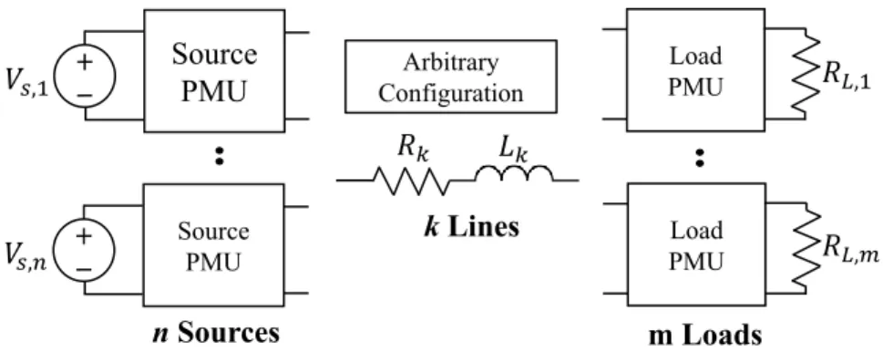
8-3 Line model. . . 135
8-4 Configuration with the highest distribution losses and voltage deviation shown in equilibrium. In terms of the existence and feasibility of an equilibrium point, this is the “worst-case” configuration that can be formed from a set of sources, lines, and loads defined as defined in Section 8.1.4. . . 138
8-5 Simple system for demonstrating small-signal stability analysis. . . . 141
8-6 Two sources and seven loads connected in the "worst case" distributed star topology. . . 147
8-7 Experimental setup with two sources and seven loads. . . 147
8-8 Experimental demonstration of equal power sharing accurate to within the precision of the testing equipment. . . 149
8-9 Experimental demonstration of realizing a specified, unequal, power sharing ratio accurate to within the precision of the equipment used. . 149
A-1 VFX converter Schematic. . . 156
A-2 VFX converter PCB layout, top and bottom layers (zoomed 2x). . . . 157
A-3 VFX converter PCB layout middle ground layer (zoomed 2x). . . 158
B-1 Source converter (synchronous boost) schematic. . . 172
B-2 Source converter PCB layout with four layers (zoomed 2.5x). . . 173
B-3 Bill of Materials of source converter. . . 174
B-4 Load converter (flyback) schematic. . . 178
B-5 Load converter PCB layout with four layers (zoomed 2.4x). . . 179
B-7 Capacitively isolated load converter schematic . . . 189 B-8 Capacitive isolaiton load converter PCB layout with four layers (zoomed
2.7x). . . 190 C-1 Resonant converter schematic. . . 196 C-2 Resonant converter PCB layout with four layers (zoomed 2.5x). . . . 197 C-3 PCB transformer used for multi-output resonant converter. . . 198 C-4 The Excel spreadsheet used to create the demand profile. . . 209 D-1 Solar panel, battery, and five load units connected to the source unit. 212 D-2 Pictures from the field trial. . . 213
List of Tables
2.1 Switch states and the voltage of the inverter in fundamental VFX mode
(Mode 1) . . . 28
2.2 Switch states and Output voltage of the inverter in the second harmonic vfx mode (mode 2) . . . 30
3.1 Components used in the experimental prototype . . . 41
3.2 Prototype converter specifications . . . 45
5.1 Common Loads . . . 67
6.1 Source converter specifications . . . 74
6.2 Source converter parameter values . . . 76
6.3 Components of the power stage of source converter . . . 78
6.4 Other components of the source converter . . . 78
6.5 Power ratings of common appliances . . . 82
6.6 Power ratings of common appliances . . . 88
6.7 Specification of components chosen for LTC3805-5 . . . 92
6.8 EMI filter Specifications . . . 96
6.9 Load converter components for 12 V power stage . . . 99
6.10 Load converter components other than the main power stage . . . 100
6.11 Safety capacitor ratings . . . 102
6.12 Capacitively isolated converter specifications . . . 105
6.13 Components used in the experimental prototype of the capacitively isolated converter . . . 110
7.1 Summary of transformer parameter measurements for cantilever model 120
7.2 Components of the 12 V power stage of the resonant converters . . . 121
7.3 Weighted efficiency metric for three converters . . . 125
7.4 System parameters and cost of components used . . . 128
7.5 Initial and lifteime cost of the system for 92% availability . . . 129
8.1 Network Specifications . . . 148
A.1 Components of VFX converter . . . 159
B.1 Components of capacitively isolated converter . . . 191
C.1 Power stage components of resonant converters . . . 197
Chapter 1
Introduction
Power electronics convert and control power and are an essential part of many elec-tronic devices and systems. Increasingly, power converters need to operate over widely varying operating conditions (voltage, current and power level), which can degrade their performance. In many applications, power converters are also being intercon-nected to form power systems. This is challenging as the converters may be conintercon-nected to operate in various configurations. In order to ensure best performance, power con-verters and systems need to adapt to the operating conditions by adjusting topology, component values or control characteristics.
The two main applications considered in this thesis are grid-interface power sup-plies and off-grid electrification. Improvements in these applications will have a signif-icant impact on power utilization from the existing grid infrastructure, and will help define the future of power utilization where this infrastructure does not exist. The techniques and designs developed, in this thesis, for adaptable and efficient operation of power converters and systems can be easily extended to other applications.
1.1
Motivation
1.1.1
Efficient universal input power supplies
More than 3 billion power supplies were sold worldwide in 2014 [1], with efficiencies ranging from 50-90% [2]. It is estimated that power supply losses account for 20-70% of all the energy that electronic products consume; with more than 3.5 billion power supplies currently being used only in the US, this amounts to about 3-4% of all US electricity usage [6]. A major portion of these power supplies are universal input power supplies (designed to operate at AC line voltages found globally). The importance of universal input power supply design has increased significantly in the recent past because of global market expansion and wide adoption of portable electronics. In this thesis, a technique to improve efficiency of universal input power supplies, without increasing cost, is presented.
1.1.2
Ad hoc microgrids for off-grid electrification
Even though centralized ac grid infrastructure is widespread, access to electricity is still a concern in large parts of the developing world. Today, about one out of every 5 people, i.e. more than 1.3 billion people in the world, do not have access to electricity and are denied a basic standard of living [3]. This deficiency impedes most aspects of human development: health, education and economic development.
It is estimated that people who don’t have access to electricity spend around 10-30% of their household income on fuel-based lighting [7]. Moreover, around a bil-lion people are served in health facilities without electricity and cannot get adequate healthcare [8]. Furthermore, approximately 50% of children in the developing world attend schools that do not have access to electricity, which limits their learning ex-perience [8]. Thus access to energy is crucial to improving the standard of living in developing countries.
With declining solar panel, battery and power electronics costs, the economic viability of distributed generation has improved. This opens up many new ways
of interacting with the grid or enabling energy access. The microgrids currently being deployed in off-grids areas in the developing world are centralized (with all the generation and/or storage co-located), which increases the distribution cost and limits the type of power sources connected to the grid.
In this thesis, a low-cost ad hoc microgrid architecture is developed that enables quick deployment of modular microgrids.
1.2
Background and Thesis Contribution
1.2.1
Efficient universal input power supplies
A trend in power electronics has been to strive for high power density and high ef-ficiency across a wide operating range [9]. High power density can be achieved by switching power converters at a high frequency. At these high frequencies, resonant converters use soft switching (i.e. Zero Voltage Switching (ZVS) and/or Zero Cur-rent Switching (ZCS)) to reduce switching losses to achieve high efficiency [10], [11]. Although soft-switched resonant converters can achieve high efficiency at a nominal operating point, the efficiency tends to degrade considerably with variations in input voltage, output voltage and power level [12].
Resonant converters commonly use frequency control [10], [11] and/or phase shift control [13] to compensate for variations in input voltage and power levels. If switch-ing frequency is increased to reduce output power or gain of the converter, such as in a series resonant converter operated above resonance to maintain ZVS, switching losses increase. Also, with operation over a wide frequency range as often required in resonant converters, the magnetics cannot be optimally designed. Furthermore, circulating currents may increase proportionally as load is decreased, resulting in higher losses at light loads. With phase shift control, operation over a wide range is likewise challenging. In many resonant converters, when two legs of the inverter are phase shifted with respect to each other, they have asymmetrical current levels at the switching transitions. The leading inverter leg can lose ZCS and the lagging leg can
lose ZVS. Other control techniques such as asymmetrical current mode control [14] and asymmetrical duty cycle PWM control [15] also have limitations, such as loss of ZVS.
In this thesis, a new technique, termed as Variable Frequency Multiplier (VFX) is introduced and its effectiveness is demonstrated for a universal input power supply. In the VFX technique, additional "frequency multiplier" modes of operation of the in-verter and/or rectifier are used to provide additional sets of operating characteristics for the converter to achieve and maintain high performance across a wide operat-ing range. Frequency multiplier circuits are often used in extreme high-frequency
RF applications (e.g., where transistor 𝑓𝑇 is a concern), and are sometimes used in
switched-mode inverters and power amplifiers ( [16], [17]). While it has been proposed to employ frequency multipliers in dc-dc converters ( [18], [19]), this is not usually done, as the output power of a frequency multiplier inverter is inherently low rela-tive to the needed device ratings. However, frequency multiplication is used here as an additional operating mode of the inverter and/or rectifier, for wide-range voltage and/or power conditions. In this context, frequency multiplication can be used to extend the efficient operating range of a converter and to improve its performance across power and voltage.
The proposed VFX technique can be applied to the inverter and/or rectifier, for a wide input and/or output voltage range. In this thesis, its use is demonstrated for a wide input voltage range using VFX operation of the inverter, and it is shown how this technique can be applied to the rectifier. Universal input power supplies need to operate over a wide input voltage range, making it extremely challenging to design resonant power converters for such a wide range of operation. So, a VFX technique is demonstrated, which is employed in the inverter of an LLC resonant converter that is designed to operate across a 4:1 input voltage range of 85 V to 340 V. It enables rescaling of operation between 120 Vac (nominal) and 240 Vac (nominal) systems, making it particularly effective in meeting world-wide voltage standards, without adding more components.
1.2.2
Ad hoc microgrids for off-grid electrification
The lack of electricity is one of the most pressing concerns in the developing world. While there is a significant need to provide electricity access, the current technologies have not been able to scale to serve these areas. In developing countries, grid electric-ity is often unreliable or entirely unavailable. The governments of these countries do not have the financial resources to increase generation to meet increasing demand in grid-connected areas, let alone to electrify off-grid areas. Also, grid extension to small or remote areas can be very expensive [20]. The deployment of individual systems (such as solar home systems and diesel generators) have seen growth in recent years due to ease of deployment [21]. However, they are very expensive and require complex financing solutions. Moreover, it is difficult to extend their operation beyond what they have been originally designed for (usually only lighting and cellphone charging in a signle household). Recently, centralized microgrids (all the generation and storage are co-located) have received more attention, especially in the developing world, due to the relatively low cost of electricity achieved by aggregate generation [22]. However, centralized microgrid development has its own challenges. Centralized microgrids re-quire a high upfront capital investment to set up, leading to expensive and complex financing. Also, they traditionally require rigorous planning and participation of a large percentage of the community to be financially feasible.
Work done by Sanders et al. [23] develops a new microgrid architecture with distributed storage, however, as all the generation is co-located, a high voltage step-up for distribution is needed to reduce distribution costs. This high voltage step-step-up is costly and requires additional safety measures.
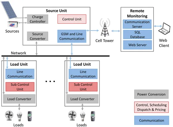
In this work, an ad hoc modular microgrid architecture is developed and field-tested. Contrary to how conventional power systems are designed, these microgrids do not require pre-planning and can operate in any network configuration. Smart power management units (PMUs) have been designed to arbitrarily connect power sources and loads, forming an autonomous microgrid. Accurate power sharing of multiple power sources is demonstrated. A methodology to attain the lowest system
cost by designing power converters that reduce lifetime energy loss has also been developed. This enables affordable and reliable electricity to be provided in off-grid areas.
1.3
Thesis Organization
The remainder of this thesis is organized as follows. The second chapter introduces the VFX technique and its application to bridge-type inverters and rectifiers. The third chapter presents the VFX technique applied to the dc-dc power stage of a universal input power supply and presents experimental results showing its high degree of effec-tiveness in this application. The fourth chapter introduces energy access and presents a case for the introduction of low-voltage dc microgrids for off-grid areas. Chapter 5 explains the ad hoc microgrid architecture that is developed. Chapter 6 deals with the design of the low-cost converters to support this dc microgrid architecture and provides details of the first prototypes built. Chapter 7 presents improvements in the design of the load converters to reduce system cost. Chapter 8 deals with the stability and power flow control of ad hoc dc microgrids. Chapter 9 concludes the thesis and presents recommendations for future research.
Chapter 2
Variable Frequency Multiplier
Technique
The Variable Frequency Multiplier (VFX) technique can be applied to the inverter stage and/or rectifier stage of a resonant converter to achieve a wide input voltage and/or output voltage range operation, or to extend the efficient operating power range. In this technique, the duty ratio and the switching frequency of an inverter and/or rectifier is changed, as input and/or output voltages change such that it pro-cesses power between dc and a specific harmonic of its switching frequency (rather than just its fundamental harmonic) to create different modes of operation. By op-erating between dc and a higher harmonic, the dc-ac (or ac-dc) voltage gain of the inverter or rectifier changes, resulting in an added operating mode with different transfer characteristics. In the case of a frequency controlled converter, this allows the converter to be operated over a narrower (intermediate ac) frequency range for a wide voltage conversion range and/or power range. Depending on the circuit archi-tecture, more than two modes can be created.
This chapter describes the mathematics of the VFX technique along with its application to the inverter stage and/or rectifier stage of resonant or other ac-link converters. To demonstrate the utility of this technique, we have built an LLC con-verter with a two-mode VFX technique applied to the incon-verter stage to efficiently extend the input voltage range of the converter. This would make the power stage
suitable for use in a "universal input" converter operable at 120 or 240 Vac, while only requiring a narrow-range design of the tank circuit (e.g., suitable for 120 Vac operation), thereby improving achievable efficiency. Aspects of this work have also been reported in publication [24].
2.1
Technique Applied to an Inverter
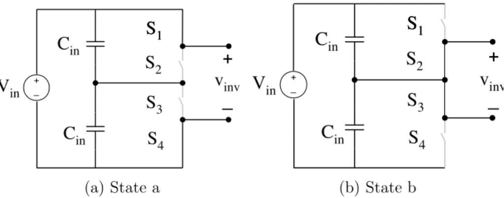
To understand the VFX technique applied to an inverter, consider the stacked bridge
inverter as shown in Fig. 2-1 with an output voltage 𝑣𝑖𝑛𝑣 (𝑣𝑖𝑛𝑣 = 𝑣𝑖𝑛𝑣1+ 𝑉𝑏𝑢𝑠− 𝑣𝑖𝑛𝑣2).
v
inv1 + _V
inS
1S
2S
3S
4C
inC
inv
inv2v
inv+
_
+
_
+
_
V
busFigure 2-1: Stacked bridge inverter with input voltage 𝑉𝑖𝑛 and output voltage 𝑣𝑖𝑛𝑣.
This inverter under VFX control operates in two modes: Fundamental VFX mode (mode 1) and second harmonic VFX mode (mode 2). This change in mode is synthe-sized by changing the switching pattern of the inverter switches and it results in an
output voltage (𝑣𝑖𝑛𝑣) which is of a different magnitude, hence, it changes the voltage
gain of the inverter. In mode 1, there are two switching states in one switching period, as summarized in Table 2.1. In state "a" switches 1 and 4 are on, and in state "b" switches 2 and 3 are on, as shown in Fig. 2-2. Mode 1 results in twice the amplitude of the individual inverter outputs, as shown in Fig. 2-3.
Table 2.1: Switch states and the voltage of the inverter in fundamental VFX mode (Mode 1)
State On switches 𝑣𝑖𝑛𝑣
a 1, 4 𝑉𝑖𝑛
+ _ Vin S1 S2 S1 S3 S4 Cin Cin vinv + _ (a) State a + _
V
inS
1S
2S
1S
3S
4C
inC
inv
inv+
_
(b) State bFigure 2-2: Stacked bridge inverter with input voltage 𝑉𝑖𝑛 and output voltage 𝑣𝑖𝑛𝑣 in
mode 1. v inv1 vinv2 V in/2 Vin/2 v inv Vin a Vbus b 0.5T T t
Figure 2-3: Output voltages of the two inverters 𝑣𝑖𝑛𝑣1 and 𝑣𝑖𝑛𝑣2 and the resulting
inverter voltage 𝑣𝑖𝑛𝑣 in Mode 1.
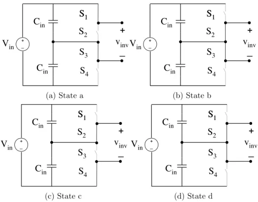
In mode 2, there are four switching states in one switching period, as summarized in Table 2.2. The VFX mode results in half the dc-to-ac voltage gain and double the frequency of the output waveform for a single switching cycle, as shown in Fig. 2-5. Thus, for the transformation stage to see the same frequency as in mode 1 (i.e.,
the same frequency of inverter output 𝑣𝑖𝑛𝑣), the converter is operated at half the
switching frequency of mode 1 (with each switching device operating at half the rate of the output ac waveform).
To create the switching patterns discussed above, and to extend this to other topologies, frequency analysis is useful. Considering Fourier analysis, the square pulse output of inverter 1 (Fig. 2-6) can be expressed as the following Fourier series:
+ _
V
inS
1S
2S
1S
3S
4C
inC
inv
inv+
_
(a) State a + _V
inS
1S
2S
1S
3S
4C
inC
inv
inv+
_
(b) State b + _V
inS
1S
2S
1S
3S
4C
inC
inv
inv+
_
(c) State c + _V
inS
1S
2S
1S
3S
4C
inC
inv
inv+
_
(d) State dFigure 2-4: Stacked bridge inverter with input voltage 𝑉𝑖𝑛 and output voltage 𝑣𝑖𝑛𝑣 in
mode 2.
Table 2.2: Switch states and Output voltage of the inverter in the second harmonic vfx mode (mode 2) State On switches 𝑣𝑖𝑛𝑣 a 1, 3 𝑉𝑖𝑛/2 b 2, 3 0 c 2, 4 𝑉𝑖𝑛/2 d 2, 3 0 𝑣𝑖𝑛𝑣1 = 𝐷1𝑉𝑖𝑛 2 + ∞ ∑︁ 𝑛=1 𝑉𝑖𝑛 𝜋𝑛𝑠𝑖𝑛(𝑛𝜋𝐷1)𝑐𝑜𝑠( 2𝜋𝑛𝑡 𝑇 ). (2.1)
Here, 𝑉𝑖𝑛 is the input voltage, 𝑇 is the switching period and 𝐷1 is the duty ratio
of inverter 1. The output of inverter 2 (𝑣𝑖𝑛𝑣2) is described by a similar equation but
with duty ratio 𝐷2.
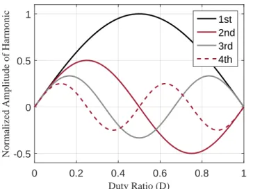
Figure 2-7 shows the amplitude of the fundamental harmonic of this waveform and several harmonic voltages as a function of the selected duty ratio. The amplitude
has been normalized to the maximum amplitude (2𝑉𝑑𝑐
v
inv1v
inv2V
in/2
V
in/2
a
b
c
d
V
busV
in/2
v
invt
0.25Ta
0.5T 0.75T TFigure 2-5: Output voltages of the two inverters 𝑣𝑖𝑛𝑣1 and 𝑣𝑖𝑛𝑣2 and the resultant
inverter voltage 𝑣𝑖𝑛𝑣 in Mode 2.
D
1T/2
V
in/2
t
v
inv1T
-D
1T/2
Figure 2-6: Square pulse train output (𝑣𝑖𝑛𝑣1) with duty cycle 𝐷1 and time period T.
0 0.2 0.4 0.6 0.8 1 Duty Ratio (D) -0.5 0 0.5 1
Normalized Amplitude of Harmonic
1st 2nd 3rd 4th
Figure 2-7: Normalized amplitude of the first four harmonics of a rectangular wave with duty ratio D.
of the half bridges correctly, the desired output can be synthesized, while canceling (or reducing) undesired frequencies. In mode 1, the fundamental of the half-bridge
inverter waveforms have to be reinforced. Hence, the duty ratios 𝐷1 = 0.5 and
𝐷2 = 0.5 are chosen. As the output is the difference between the inverter output
voltages (𝑣𝑖𝑛𝑣1 and 𝑣𝑖𝑛𝑣2), to reinforce these waveforms, the two half bridges have to
be switched 180𝑜 out of phase, as shown in Fig. 2-3 and expressed in Equation (2.2).
𝑣𝑖𝑛𝑣1 = 𝑉𝑖𝑛 2 + ∞ ∑︁ 𝑛=1 2𝑉𝑖𝑛 𝜋𝑛 𝑠𝑖𝑛(𝑛𝜋0.5)𝑐𝑜𝑠( 2𝜋𝑛𝑡 𝑇 ). (2.2)
In mode 2, the second harmonic has to be reinforced, hence, 𝐷1 = 0.25and 𝐷2 =
0.75 are chosen, which results in the maximum amplitude of the second harmonic,
while canceling out the fundamental component. As the output voltage of the inverter
is the difference between the two half bridge inverter voltages (𝑣𝑖𝑛𝑣1 and 𝑣𝑖𝑛𝑣2), to
reinforce the second harmonic, the fundamentals of the two waveforms are in phase, as seen from Fig. 2-7. In this mode, the fundamental harmonic of the half bridge waveforms is canceled while the second harmonic is reinforced so the output frequency doubles while the output amplitude is halved, as shown in Fig. 2-5 and expressed in Equation (2.3). 𝑣𝑖𝑛𝑣1 = 𝑉𝑖𝑛 4 + ∞ ∑︁ 𝑘=1 2𝑉𝑖𝑛 𝜋𝑘 𝑠𝑖𝑛(𝑘𝜋0.5)𝑐𝑜𝑠( 2𝜋𝑘𝑡 𝑇 ), (2.3)
where 𝑘 = 2𝑛. It should be noted that the dc component of the inverter output is different in the two modes, which imposes a rebalancing of blocking capacitor voltages when the operating mode is switched. For the same output frequency, the two inverters switch at half the output frequency. Note that in each case (for the two-mode VFX inverter), the ac output waveform is a square wave. This technique can thus be used in many kinds of ac link topologies, including all kinds of resonant converters and dual-active bridge converters.
2.2
Technique Applied to a Synchronous Rectifier
A rectifier receives an ac current (or voltage) at its input and presents an ac voltage (or current) at its input, which results in dc power being absorbed and delivered to the output as dc voltage and current. The amount of power absorbed depends on the amplitude of the voltage (or current) presented at the input of the rectifier. Hence, the VFX technique can likewise be applied to the rectifier to make the ac voltage at its input be either at the fundamental of the rectifier devices’ switching frequency or at a harmonic of the devices’ switching frequency in order to convert the ac input power to dc.
Q
3
Q
4
Q
1
Q
2
v
R1
v
R2
R
L
C
o
I
Ro
+
V
Ro
-v
Ri
=v
R1
-v
R2
Figure 2-8: Full bridge synchronous rectifier with a resistive output load. For example, consider a full bridge synchronous rectifier as shown in Fig. 2-8. Similar to the inverter presented in the previous section, we can create two modes of
operation by changing the switching pattern of 𝑄1, 𝑄2, 𝑄3 and 𝑄4, which determines
the rectifier input voltage. In mode 1, the input voltage of leg 1 of the rectifier (𝑣𝑅1)
is equal to the rectifier output voltage (𝑉𝑅𝑜) for half the switching cycle (𝑄1 and 𝑄4
second half of the switching cycle (𝑄2 and 𝑄3 switched on), 𝑣𝑅2 is equal to 𝑉𝑅𝑜 and
𝑣𝑅1 is zero, as shown in Fig. 9. The resulting voltage at the input of the rectifier 𝑣𝑅𝑖
is the difference of the input voltages of the two rectifier legs (𝑣𝑅𝑖 = 𝑣𝑅1− 𝑣𝑅2) and is
either +𝑉𝑅𝑜 or −𝑉𝑅𝑜 with 50% duty ratio. The voltage waveform at the input of the
rectifier (Fig. 2-9), can be used to determine the ac-to-dc voltage gain of the rectifier in mode 1. 𝑀𝑅,𝑚𝑜𝑑𝑒1 = 𝑉𝑅𝑜 𝑣𝑅𝑖,𝑝𝑘−𝑝𝑘 = 𝑉𝑅𝑜 2𝑉𝑅𝑜 = 0.5. (2.4) vRi +VRo vR1 -VRo vR2 0.5T T 1.5T +VRo t +VRo
Figure 2-9: Voltage waveforms at the rectifier input during mode 1.
In mode 2, 𝑣𝑅1 is equal to 𝑉𝑅𝑜 for 75% duty cycle and 𝑣𝑅2 is phase shifted by 90
degrees of the fundamental (a quarter of the period T) and equal to 𝑉𝑅𝑜 for 25 % duty
cycle. The resulting rectifier input voltage 𝑣𝑅𝑖 has twice the frequency at which the
rectifier switches operate, and is either 𝑉𝑅𝑜or 0. In order to have the same input (ac)
voltage frequency as mode 1, the rectifier switches are switched at half the frequency of mode 1 (with all devices operating at the same frequency). The resulting voltage waveforms are shown in, Fig. 2-10 and as seen from the figure, the ac-to-dc voltage gain of the rectifier doubles in mode 2.
𝑀𝑅,𝑚𝑜𝑑𝑒2 = 𝑉𝑅𝑜 𝑣𝑅𝑖,𝑝𝑘−𝑝𝑘 = 𝑉𝑅𝑜 𝑉𝑅𝑜 = 1. (2.5)
This gives us a number of design opportunities. For example, one can operate the converter with double the output voltage (if the input voltage remains the same), effectively increasing the output voltage range of the converter.
+VRo vRi +VRo vR1 +VRo vR2 0.75T 0.25T 0.5T T T T 0.5T 0.25T t
Figure 2-10: Voltage waveforms at the rectifier input during mode 2.
With the rectifier driven by a nearly sinusoidal current waveform (due to a resonant tank in a resonant converter), the amount of power transferred by controlling the phase difference between the current and the input voltage of the rectifier can be controlled. Consider a simplified case where the input voltage and current are in phase, using Fundamental Harmonic Approximation (FHA) the effective input of the
rectifier can represented as an equivalent resistor (𝑅𝑒𝑞𝑣 = 𝑘0𝑅𝐿), where 𝑅𝐿 is the
output load resistor, and 𝑘𝑜 is a constant that depends on the ratio between the
fundamental harmonic of the voltage and the current.
In mode 1, the fundamental frequency components of the voltage waveform and the current waveform for the rectifier shown in Fig. 2-9 are given by:
𝑣𝑅𝑖−𝑎𝑐,𝑚𝑜𝑑𝑒1 = 4 𝜋𝑉𝑅𝑜𝑠𝑖𝑛(𝜔𝑡). (2.6) 𝑖𝑅𝑖−𝑎𝑐,𝑚𝑜𝑑𝑒1 = 𝜋 2𝐼𝑅𝑜𝑠𝑖𝑛(𝜔𝑡). (2.7)
cur-rent. The ratio of the ac voltage and current, representing the equivalent resistance, is given as: 𝑅𝑒𝑞𝑣,𝑚𝑜𝑑𝑒1 = 𝑣𝑅𝑖−𝑎𝑐,𝑚𝑜𝑑𝑒1 𝑖𝑅𝑖−𝑎𝑐,𝑚𝑜𝑑𝑒1 = 8 𝜋2𝑅𝐿. (2.8)
Where 𝑅𝐿 is the dc load resistor at the output of the rectifier, equal to 𝑉𝑅𝑜/𝐼𝑅𝑜
(for continuous steady-state operation). Using the two-mode VFX technique, we alter the rectifier characteristics (while still operating with a “resistive" characteristic) by changing the switching pattern of the switches. The magnitude of the fundamental
frequency component of the ac rectifier input voltage 𝑉𝑅𝑖−𝑎𝑐 decreases by half:
𝑣𝑅𝑖−𝑎𝑐,𝑚𝑜𝑑𝑒2 =
2
𝜋𝑉𝑅𝑜𝑠𝑖𝑛(𝜔𝑡). (2.9)
For the same output power, 𝐼𝑅𝑜 decreases by half, so the input current is given
by:
𝑖𝑅𝑖−𝑎𝑐,𝑚𝑜𝑑𝑒2= 𝜋𝐼𝑅𝑜𝑠𝑖𝑛(𝜔𝑡). (2.10)
Hence, the equivalent resistance is equal to:
𝑅𝑒𝑞𝑣,𝑚𝑜𝑑𝑒1 =
2
𝜋2𝑅𝐿. (2.11)
The second operating mode in VFX gives us the opportunity to adjust the voltage and current profile of the rectifier (e.g., keeping an equivalent ac input resistance at a different dc output voltage, or changing the effective ac output resistance for a given dc resistive loading on the rectifier).
The two-mode VFX technique presented can be easily extended to higher modes, given an appropriate rectifier structure. It can likewise be applied to many other rectifier topologies, such as stacked rectifiers, voltage-fed rectifiers, current-doubler rectifiers, etc.
Chapter 3
VFX Technique Applied to the Dc-Dc
Converter of a Power Supply
The proposed VFX technique is demonstrated in a dc-dc converter stage designed for a universal-input laptop power supply. The ac voltage varies in different countries but the nominal voltage is either 110-120 Vrms at 60Hz, or 220-240 Vrms at 50 Hz. Therefore, 120 Vrms and 240 Vrms have been selected as the nominal upper limits for the two modes of converter operation, corresponding to peak dc voltages of 170 V and 340 V applied to the dc-dc converter. The VFX technique is very useful for this application because there are two distinct peak input voltages separated by a factor of two in amplitude, allowing us to use the VFX technique to rescale them to a common range at the resonant tank.
An LLC converter has been selected for the dc-dc stage [25]. It uses frequency control to regulate the output voltage and has many advantages. The main advantage is that it has the capability to regulate the output voltage over a wide range of input voltage and power with only a small variation in the switching frequency. Also, it achieves zero voltage switching (ZVS) over the entire range of operation, thus reducing the switching losses. Moreover, the leakage and magnetizing inductance of the transformer can be incorporated into the design.
Figure 3-1 shows the schematic of the LLC converter, which has been implemented with a stacked-bridge inverter appropriate for voltage step-down and VFX operation.
As the input voltage is high, stacked half bridges are used, with the resonant
capac-itor 𝐶𝑟 also serving as a blocking capacitor. This reduces the voltage stress of the
transistors by half as compared to a non-stacked full bridge or half bridge, which increases the performance with available high-frequency devices. The transformation
stage consists of a series inductor (𝐿𝑟), a capacitor (𝐶𝑟) and a parallel inductor (𝐿𝑚).
The capacitor not only provides resonant filtering but also provides dc blocking for flux balancing.
C
rL
rL
mn:1
D
1D
2+
V
out _S
1S
2S
1S
3S
4C
inC
in + _V
inI
rI
m+V
cr-
V
inV
in2
2
+
_
+
_
V
busFigure 3-1: Schematic of the LLC converter with a stacked bridge inverter incorpo-rating the VFX technique.
The transformer leakage and magnetizing inductance can be used instead of sep-arate inductors [26]. A center-tapped transformer is used to reduce the number of series diodes in the rectification path. This increases the loss of the transformer and the voltage stress of the diodes. However, this trade-off is still beneficial because of the low output voltage. Synchronous rectification can be used to further reduce losses in the rectification stage [27], [28], [29] but was not used here. The converter is de-signed using the method outlined in [30], as described in detail below. Fundamental harmonic analysis (FHA) is used to analyze and design the converter. Time-based [31] and approximate methods [32], [33] could be used for a more accurate gain analysis. The converter is designed for a maximum input voltage of 170 V in the
funda-mental mode and an output voltage 𝑉𝑜𝑢𝑡 of 20 V. To ensure that the power supply
(of which the dc/dc converter is the second stage) has a sufficiently high power factor (i.e., greater than 0.95), the minimum input voltage for the dc-dc stage is 85 V. For input voltages above 170 V, the second harmonic VFX mode is used to decrease the voltage that the transformation stage sees by half.
Using FHA, all the voltages and currents are represented by their fundamental components, and the secondary-side variables are reflected to the primary side to obtain the approximated circuit shown in Fig. 3-2.
Cr L r Lm or 8n2Vout 2 π2 Pout Rn= Mode 2: (1/ )π Vin Mode1: (2/ )π Vin
Figure 3-2: Fundamental harmonic model of the LLC converter.
In mode 1, the peak ac output voltage of the inverter is 𝑉𝑖𝑛/2, providing a
funda-mental ac amplitude of (2/𝜋)𝑉𝑖𝑛. Hence, the transformer turns ratio has been selected
as:
𝑛 = 𝑉𝑖𝑛−𝑚𝑎𝑥
2𝑉𝑜𝑢𝑡
= 4.25. (3.1)
The recommended range of the ratio of 𝐿𝑚/𝐿𝑟 (referred to as k) is between 3 to
10 [30]. Smaller values of 𝑘 result in a narrow and steep gain curve but cause a much higher magnetizing current, leading to higher loss. To have a reasonable minimum frequency, magnetizing current and dead time, the value of 𝑘 is chosen as 7. The value of 𝑘 can be optimized for a narrower frequency range or a higher efficiency
depending on the intended application. The maximum gain (𝑀𝑚𝑎𝑥) of the resonant
network is selected to be higher than 2, i.e, 2.4, to ensure sufficient gain, even with the inaccuracies of using fundamental harmonic analysis.
To ensure ZVS, the input impedance of the resonant network needs to be inductive at the drive frequency. The borderline between the inductive and capacitive region is when the impedance is purely resistive. By equating the imaginary part of input
impedance (𝑥−1
𝑥+
𝑥𝑘
1+𝑘2𝑥2𝑄2) equal to zero, the value of Q is found. Here, 𝑥 = 𝑓𝑖𝑛𝑣/𝑓𝑟,
where 𝑓𝑖𝑛𝑣 is the inverter output voltage frequency (which is the switching frequency
frequency (𝑓𝑟 = 2𝜋√1𝐿 𝑟𝐶𝑟). 𝑄 = √︃ 1 (1 − 𝑥2)𝑘 − 1 𝑘2𝑥2. (3.2)
Substituting the value of Q in the expression for gain 𝑀 leads to the maximum gain
(𝑀𝑚𝑎𝑥). 𝑀 = √︃ 1 (1 + 1𝑘(1 − 𝑥12)2+ 𝑄2(𝑥 − 1 𝑥)2 , 𝑀𝑚𝑎𝑥= 𝑥 √︁ 𝑥2(1 + 1 𝑘) − 1 𝑘 . (3.3)
The maximum gain leads to the minimum normalized frequency. This value of
𝑥𝑚𝑖𝑛 is substituted in the expression of 𝑄 to get the maximum 𝑄 below which ZVS
is maintained. 𝑄𝑚𝑎𝑥 = 1 𝑘 √︃ 1 + 𝑘(1 − 𝑀1 𝑚𝑎𝑥2 𝑀𝑚𝑎𝑥2− 1 = 0.1706. (3.4)
The values of 𝑛, 𝑘, 𝑅𝑛 and 𝑄𝑚𝑎𝑥 are used to calculate target values of 𝐿𝑟, 𝐿𝑚 and
𝐶𝑟: 𝐿𝑟 = 𝑄𝑚𝑎𝑥𝑅𝑛 𝜔𝑟 = 6.36𝜇𝐻, 𝐿𝑚 = 𝑘𝐿𝑟 = 44.5𝜇𝐻, 𝐶𝑟= 1 𝑄𝑚𝑎𝑥𝑅𝑛𝜔𝑟 = 15.9𝜇𝐹. (3.5)
The dead-time should be sufficient such that the current in the inductor 𝐿𝑚 at the
switching instant can discharge the voltage on the MOSFET before it is switched on.
By equating the charge required to the current in inductor 𝐿𝑚 during the dead time,
the deadtime is calculated as 𝑡𝑑 = 8𝐶𝑑𝑠𝑓𝑟𝐿𝑚 = 62𝑛𝑠. Using FHA, the gain curve of
If the converter had been designed without considering the VFX technique as a half bridge implementation, the operating voltage range would have been 85 V to 340 V. This results in the transformer being designed for double the transformer turns ratio, 8.5 rather than 4.25, as calculated from Equation (3.1). Also, the maximum
gain (𝑀𝑚𝑎𝑥) of the transformation stage would have to be doubled, 4 rather than
2, resulting in higher inductor losses. The rest of the components would remain the same. Hence, this would result in an increase in losses.
3.1
Experimental Prototype and Results
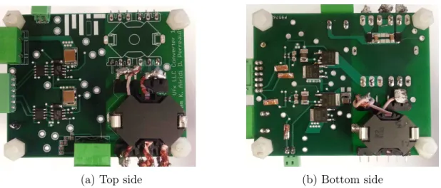
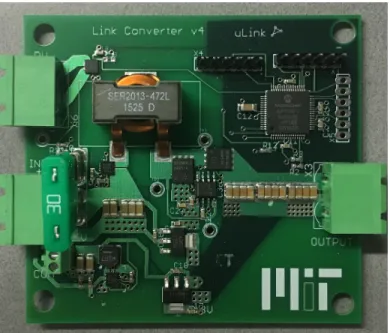
Using the design values from the previous section, a prototype for the converter was built, as seen in Fig. 3-4. The components used for the experimental prototype are summarized in Table 3.1. Full detailed schematics, along with components used and illustrations of the circuit board layout are provided in Appendix A.
Table 3.1: Components used in the experimental prototype
Components Type
Controller 150 MHz digital signal controller (TI’s TMS320F28335)
Signal Isolators 150 Mbps two channel digital isolator (NVE Corporation’s IL711), Qty: 2 Gate Drivers 600-V/4-A High and low side gate driver (IR’s IRS21867), Qty: 2
Transistors 200-V/34-A OptiMos power transistor (Infineon’s IPD320N20N3), Qty: 4 Capacitors Cr: 15.99 pF/250 V COG, Cout: 20 𝜇F/25-V, Cin: 1 𝜇F/250-V Qty: 2 Inductors Lr: 3.6 𝜇H, RM8A100 3F3 core, litz wire (6 turns, 48 AWG, 1000 strands). Transformer RM10A160 3F3 core, Primary litz wire (17 turns, 46 AWG, 450 strands).Secondary litz wire (4 turns, 46 AWG, 450 strands). Diodes 60-V/3-A Schottky diode (NXP’s PMEG6030), Qty: 2
The dc-dc converter is a step-down converter operating at the series tank (𝐿𝑟, 𝐶𝑟)
resonant switching frequency (𝑓𝑟) of 500 kHz. It has an input voltage range of 85
V - 340 V, fixed output voltage of 20 V and a rated output power of 50 W. Table 3.2 summaries the converter specifications. To control the output power and gain, frequency control is utilized, while the appropriate VFX mode is used based on input voltage being above or below 170 V (in the laptop power supply case, one can either select the mode based on instantaneous voltage, or more effectively based on detection
0.2 0.4 0.6 0.8 1 1.2 1.4
Normalized inverter output frequency, x
0.5 1 1.5 2 2.5
Gain of the resonant network,
M
(a) The gain (M) of the transformation stage using FHA. It has a peak gain at inverter output voltage fre-quency (𝑓𝑖𝑛𝑣) of 0.4 times the resonant tank (𝐿𝑟 and 𝐶𝑟) frequency.
0.5 1 1.5
Normalized inverter output frequency, x
0 0.05 0.1 0.15 0.2 0.25 0.3
Gain of the converter, V
out
/V
in Mode 1
Mode 2
(b) The gain of the converter (𝑉𝑜𝑢𝑡/𝑉𝑖𝑛) using FHA.
Mode 1 has twice the voltage gain of Mode 2.
Figure 3-3: Voltage gain of (a) the transformation stage and (b) converter, using FHA.
of the ac line voltage range in use). The transformer was designed to exploit the integrated magnetizing inductance. The leakage inductance was used as part of the resonant inductance. However, this was insufficient and a series inductor was added to provide the required series resonant inductance.
(a) Top side (b) Bottom side
Figure 3-4: Picture of the (a) top side and (b) bottom side of the prototype board. Vds (S4) Vgs (S4) Ir t: 400 ns, Vgs: 5 V, Vds: 20 V, Ir: 500 mA (a) At 340 V in mode 1 Vds (S4) Vgs (S4) Ir t: 1 us, Vgs: 5 V, Vds: 20 V, Ir: 1 A (b) At 170 V in mode 1 Vds (S4) Vgs (S4) Ir t: 1 us, Vgs: 5 V, Vds: 50 V, Ir: 500m A (c) At 340 V in mode 2 Vds (S4) Vgs (S4) Ir t: 2 us, Vgs: 5 V, Vds: 50 V, Ir: 500 mA (d) At 170 V in mode 2
Figure 3-5: Current and voltage waveforms of the converter at 50 W when operated in mode 1, fundamental mode, and in mode 2, VFX mode. (1-Blue) Gate voltage
of switch 𝑆4, (2-Turquoise) drain-source voltage of switch 𝑆4, and (4-Green) current
100 150 200 250 300 350 Input voltage (V) 80 85 90 95 100 Efficiency (%) Mode 1 Mode 2
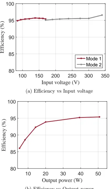
(a) Efficiency vs Input voltage
10 20 30 40 50 Output power (W) 80 85 90 95 100 Efficiency (%)
(b) Efficiency vs Output power
Figure 3-6: Efficiency of the converter (a) with variation in input voltage with fixed output voltage and 50 W output power operating in mode 1 and 2, and (b) with variation in output power with 170 V input voltage and fixed output voltage operating in mode 1.
Table 3.2: Prototype converter specifications
Parameter Value
Input voltage (𝑉𝑖𝑛) 85-340 V
Output voltage (𝑉𝑜𝑢𝑡) 20 V
Output power (𝑃𝑜𝑢𝑡) 5 W-50 W
Nominal Switching frequency (𝑓𝑟) 500 kHz
across the entire range of operation. The switching waveforms for input voltages of 170 V and 85 V at 50 W in mode 1 are given in Fig. 3-5 (a) and (b), respectively. It shows the current input to the transformer primary, which is also the output current
of the bottom inverter, the gate drive voltage of switch 𝑆4 and the drain-source
voltage of switch 𝑆4. At 170 V (Fig. 3-5 (a)), the current is sinusoidal with a cusp at
the switching instants. The converter was operated below resonance, to increase the gain of the transformation stage, as the input voltage decreased. As the converter is operated away from resonance, the current waveform distorts and does not remain sinusoidal. However, the experimental gain is very similar to that calculated by using FHA and ZVS is still maintained.
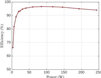
For input voltages above 170 V, operation is changed to the VFX mode and the waveforms for 170 V and 340 V are given in Fig. 3-5 (c) and (d), respectively. The converter is operated at half the normal-mode switching frequency, which decreases the frequency-dependent switching losses, and ZVS is still maintained, resulting in high efficiency.
The efficiency of the converter was measured across input voltage in both modes and across output power. The measured efficiency of the converter at rated power, as a function of input voltage, is plotted in Fig. 3-6 (a). The converter continues to operate with high efficiency across the two modes, and the converter efficiency varies from 94.9% to 96.6% . The measured efficiency as a function of output power and fixed input voltage of 170 V in fundamental mode varies from 86% to 95.4% and is plotted in Fig. 3-6 (b). The high efficiency over a wide operation range demonstrates the effectiveness of the VFX technique.
3.2
Conclusion
In this chapter, the VFX technique is applied to the inverter of an LLC converter, to demonstrate the effectiveness of this technique for universal input power supplies. This technique increases the input voltage range by a factor of two, and the converter achieves high efficiency over a wide range of operation. The experimental prototype is able to achieve an efficiency of 94.9% to 96.6% across the entire input voltage range at 50 W output power, and 86% to 95.4% across a 10:1 power range with 170 V input voltage. Hence, the VFX technique can be very useful to obtain high efficiency across a wide range of operation.
Chapter 4
A Case for Innovation in Electricity
Access
4.1
Understanding Energy Access
Access to affordable energy is crucial for economic and human development. There is no single agreed upon definition of energy access. The International Energy Agency, in the World Energy Outlook, [34] defines modern energy access as: "a household having reliable and affordable access to clean cooking facilities and to a minimum level of electricity consumption which is increasing over time" where the minimum level of electricity is assumed to be 250 kWh per year for a rural household and 500 kWh per year for an urban household. As this definition of energy access is difficult to measure, there is significant variation in the statistics quoted by different sources. Although energy access involves both cooking facilities and electricity, the focus of this thesis will primarily be on electricity access. Here, electricity access is analyzed within the context of off-grid areas in developing countries, and the provision of a basic level of electricity to run the essential electronics of modern day: lights, fans, cell phones and/or other small electronics.
The ideal solution for electricity provision would be to provide consumers with uninterrupted and virtually unlimited access to electricity, as is the norm in developed countries where around the clock electricity is considered a basic necessity. However,
this is not possible in off-grid parts of developing countries due to the high cost of the grid infrastructure needed, and the limited availability of financial resources. Additionally, in off-grid areas, there is not even a demand for such high powered access as there is limited purchasing power to acquire and run high power appliances. Hence, there’s a need for metrics to define what electricity means in different contexts. The World Bank has attempted to measure and classify access to electricity through a multi-tier approach [35]. This approach divides provision of electricity into two 5-tier indices. The first index is based on electricity supply and the second index is based on electricity services. Electricity supply is measured according to the metrics of peak available capacity, duration of usage during daytime, evening supply, affordability, legality and quality. Electricity services can be measured by metrics based on the appliances they can serve; starting simply with basic lighting and cell phone charging usage, and going upwards in power to higher powered appliances. This approach provides a measure of energy access by weighted index, of electricity supply and services, for a certain area, and quantifies quality of service provided by different solutions, allowing comparison between different areas.
Technology developed in this thesis is easily expandable to the highest levels of service (tier 5 as per World Bank’s multi-tier approach), which does not lock off-grid areas in low energy lifestyles, and provides an opportunity for off-grid areas to expand energy access with increasing demand in the long run.
4.2
Different Approaches for Electricity Access
The preferred choice for electrification infrastructure of almost all governments is grid-based electrification. This top-down centralized approach is favored because it is a well-tested and an age-old method of electrification. Also, if done right, it can pro-vide reliable electricity and does not hamper its citizens from increasing their energy consumption and setting up economic activities with increased electricity consump-tion. However, grid extension might not always be the most economical soluconsump-tion. Transmission and distribution can be costly to set up and maintain, especially given
low electricity demand in remote areas [20]. Additionally, grid electricity is generally unreliable in developing countries. The governments of these countries do not have the financial resources to provide reliable electricity to grid connected areas or to increase generation to cope with increasing demand, let alone to provide electricity to off-grid areas. International Energy Agency estimates [21] that it will cost around $48 billion to provide universal energy access, and the gap between expected cost and available public funding is around $34 billion dollars, requiring involvement of the private sector to reduce the gap.
The private sector has employed different bottom-up decentralized approaches, such as the use of individual systems (for exmaple, solar home systems and diesel generators) and microgrids. Individual systems have seen rapid growth in the recent past due to the ease of deployment [21]. However, they are expensive and require complex financing solutions. Also it is difficult to extend their capacity beyond what they have been originally designed for i.e. usually lighting and cellphone charging only. On the other hand, microgrids can provide lower cost electricity as they aggregate generation and load, thus decreasing the cost per watt [22]. However, development of centralized microgrids (with all generation and storage co-located) has its own challenges. Centralized microgrids require a high upfront capital investment to set up, leading to expensive and complex financing. Also, they traditionally require rigorous planning and participation from a large percentage of the community to be financially feasible [36].
While there is a pressing need to provide electrification to off-grid areas, the current technologies have not been able to scale to serve the vast majority of off-grid populations. The first step in the energy access ladder has been to move from kerosene or candles to solar lamps. The deployment of solar lamps has grown significantly in recent years due to their low cost, however, they only provide light (and sometimes cell phone charging) rather than a source of electricity [37]. The next step is the provision of electricity for basic appliances. However, the end goal should be provision of electricity with high availability, affordability, adequacy, convenience and reliability. Technological innovation with strong business fundamentals will allow this to happen.