Development and Analysis of Frequency,
High-Density PFC Power Conversion
by
Ali Saeed AlShehab
B.S., Massachusetts Institute of Technology (2014)
Submitted to the Department of Electrical Engineering and Computer Science in partial fulfillments of the requirements for the degree of
Master of Science in Electrical Engineering and Computer Science at the
THE MASSACHUSETTS INSTITUTE OF TECHNOLOGY
September, 2015
0 Massachusetts Institute of Technology 2010. All rights reserved.
Signature redacted
A uthor ... ...
Departmei-of Btecrical Engineering and Computer science
Signature redacted
September 16, 2015C ertified byJ...
...
David J. PerreaultAccepted by...
MASSACHU OF TSignature redacted
N N $ETTSINSTITUTE ECHNOLOGY Thesis SupervisorDr. Christopher Terman
Chairman, Masters of Engineering Thesis CommitteeDevelopment and Analysis of High-Frequency, High Density
PFC Power Conversion
by
Ali Saeed AlShehab
Submitted to the Department of Electrical Engineering and Computer Science in partial fulfillments of the requirements for the degree of
Master of Science in Electrical Engineering and Computer Science
Abstract
This thesis explores the design of power converters that deliver isolated low-voltage dc output (-24V) and operate from "universal" ac input voltage (85 - 264 Vac RMS).
It is important that these converters have good overall efficiency (~90-95%), and good ac line power factor (>0.9, and ideally >0.95) to better utilize the available energy. This thesis looks into achieving high efficiency, high power factor, low voltage stresses, and smaller component sizes by utilizing high frequency operation. The research focuses on component and subsystem evaluation, development and testing as a part of many-person research in this space.
The thesis presents a literature based study on current PFC circuit designs and tradeoffs. It also introduces a specific PFC architecture, which provides a low dc output voltage drawing energy from a wide range ac input voltage while maintaining a high power factor. The architecture includes two stages:
The first is a "Power Factor Correction" (PFC) which functions as an input stage drawing energy from a wide-range input current. It uses a resonant transition inverted (RTI) buck converter topology to step down the voltage from line voltage (85 - 264 Vac RMS) to around 72V. Furthermore, the inductor for the RTI buck is analyzed.
The middle stage is an energy buffer to provide the required energy level for twice line frequency energy buffering and 20ms of energy hold up. The capacitor requirements, analysis, and selection are explored and developed.
The second stage is a transformation and regulation stage which also provides electrical isolation between the ac input and dc output. The thesis also explores the use of available conventional high-density telecom "brick" converters as a second stage.
In conclusion, the project explores the possibility of using a buck configuration for the PFC, sacrificing the ability to use high energy density 400V capacitors while gaining the advantage of using the high-density telecom brick converters and different output voltage options.
Thesis Supervisor: David J. Perreault
Acknowledgements
I would like to thank my thesis supervisor Professor David Perreault whose inspiration, guidance and provision made this research project possible. I would also like to thank my colleagues at LEES especially Juan Santiago and his endless assistance throughout my year at LEES. Other LEES faculty and staff have also been an integral part of this work, including Dave Ottenwho guided me in building many of the circuitry and test setups, and Professor Khurram Afridi.
I would not have been able to accomplish this without the unlimited support of my family and friends. It is to them that this thesis is dedicated. The unconditional love and encouragement of my parents Saeed AlShehab and Zahra AlJuffairi, and my sisters Ghadeer AlShehab and Mariam AlShehab have always been a driving force for me. My brother Mohamed AlShehab has always been my best friend and source of comfort and guidance. And to my friends at MIT that made this a great and fun place to be to you all, I am truly grateful and "Thank you!"
Finally, I would like to thank the sponsors who supported this research. Much of the work was funded by OMRON.
Table of Contents
Chapter 1
Introduction ... 8
1.1. Background and Motivations ... 8
1.2. Thesis Objectives and Contributions ... 9
1.3. Thesis Organization ... 10
Chapter 2 Power Factor Correction Study ... 12
2.1. Introduction ... 12
2.2. Background ... 12
2.2.1. PFC: Concepts and Definitions ... 12
2.2.2. PFC: A Literature Based Study ... 17
2.3. Architecture of Interest ... 23
Chapter 3 Capacitor Design for Twice Line Frequency Energy Buffering ... 27
3.1. Background and Motivation ... 27
3.2. Architecture of Interest ... 28
3.3. Capacitor Energy ... 29
3.4. Capacitor Energy Buffering ... 30
3.4.1. Energy Density Constrained by Allowed Ripple ... 31
3.4.2. Energy Density Constrained by RMS Current Limits ... 34
3.4.3. Energy Density Constrained by Holdup Energy ... 39
3.5. Design Application ... 44
3.5.1 Topology of Interest ... 45
3.5.2 Capacitor Section and Conclusion ... 45
Chapter 4 Inductor Design for Resonant Transition Buck Converter ... 51
4.1. Background and Motivation ... 51
4.2. Inductance Requirement ... 52
4.2.1. Inductor Gap ... 55
4.3. Magnetic Flux Density ... 57
4.4. Inductor Losses ... 58
4.4.1. Core Losses ... 58
4.4.2. Winding Losses ... 61
4.5. Application Design ... 64
4.5.1 Experimental Results ... ... ... 68
Chapter 5 High Density High Efficiency Telecom Converters ... 71
5.1. Background and Motivations ... ... 71
5.2. Converter Selection ... ... ... ... 72
5.3. Experimental Results ... ... ... 73
Chapter 6 System Testing ... 76
6.1. 600W Zener Bank Load ... ... .76
6.1.1 Modeling and Analysis ... 76
6.1.2 Heat Sink ... ... ... 77
6.1.3 Recommendations and Experimental Results ... 78
6.2. Hold up Time Testing ... 79
Chapter 7 Summary and Conclusion ... ... 81
7.1 Thesis Sum m ary and conclusion ... 81
7.2 Recomm endations for Future W ork ... 82
References ... ... . ... 79
Appendix A .... ... ... ... 86
Chapter 1
Introduction
1.1. Background and Motivations
We are interested in power supplies which supply low dc voltage loads by drawing energy from the single-phase ac grid. These supplies have converters that deliver isolated low-voltage dc output (-12V or -24V) and operate from "universal" ac input voltage (85 - 264 Vac RMS).
Furthermore, it is important that these converters have good overall efficiency (~90-95%), and good ac line power factor (>0.9, and ideally >0.95) to better utilize the available energy. This proposal is concerned with achieving high efficiency, high power factor, low voltage stresses, and smaller component sizes by utilizing high frequency operation. The research focuses on component and subsystem evaluation, development and testing as a part of many-person research in this space.
Such converters usually operate at relatively low switching frequencies - around 200kHz or below- and have low power densities - around 10 W or below. The relatively low frequency operation results in designs which require physically large magnetic components. The size issue could be addressed by increasing the switching frequency which would allow for smaller and cheaper magnetic components. Evidently, high frequency circuit architectures coupled with advances in semiconductor devices could have a big impact on the size and cost of grid-interfaced conversion from high-to-low voltage supplies.
Hence, there is an evident need for new power electronics technologies that can meet the requirements of practical applications at far lower size and cost than is presently achievable.
When operating at high frequency one of the main concerns is switching losses. Low loss circuit designs and control methods made it possible to achieve high switching frequencies in the range of 3 to 30 MHz with good efficiency ([1 1], Fig. 1.2).
1.2.
Thesis Objectives and Contributions
This thesis will contribute to the design of a full PFC system of the type in Fig 1.1, shown below. It will focus on aspects of the high-frequency PFC portion, and will also explore selection and testing of commercial telecom converters for use in the power combining / isolation / transformation stage. In this effort, the design and testing of the high-frequency buck power stage will be the central focus, including design of miniaturized inductors for the converter and optimized selection of electrolytic capacitors to provide twice-line-frequency energy buffering and holdup energy. It will also include an experimental study of available high-density high efficiency telecom brick converters and how suitable they are to be used as the second stage converters. Regulating Converter Power AC
Rectifier
Combining Converter RegulatingT
~ConverterFig 1.1: The full PFC grid interface power conversion system architecture comprises a line-frequency rectifier, a stack of capacitors, a set of regulating converters, and a power combining
The thesis has three primary objectives in the design of a prototype high-frequency PFC system. The first objective of this thesis is to figure out the smallest capacitor that could be used for twice line frequency energy buffering as well as figure out the optimal operating point for utilizing this capacitor. The operating point includes choosing the voltage at which energy is stored, the capacitance value and the allowable ripple. The second objective is to realize the smallest inductor that could be used for the resonant transition buck converter in the high-frequency PFC stage. The third objective is to realize the possibility of using high-density and
high efficiency telecom brick DC/DC for the second isolation/transformation/configuration stage.
The thesis makes several contributions. The first contribution is a study, comparison and experimental evaluation of capacitors for twice-line frequency energy buffering and holdup in our proposed PFC system. Such capacitors are important because they represent a substantial fraction of converter volume. A second contribution is a study, comparison and experimental evaluation of inductors for the resonant-transition inverted buck PFC stage. This will include evaluation of various magnetic materials and inductor designs and their comparison in high-frequency power stages. This is important because miniaturization of the magnetics is a key goal. Moreover, the thesis includes development of a test stand for evaluating designs of the frequency PFC stage (resonant-transition inverted buck design), including design of a high-power 600 W load to absorb energy from the converter during testing and development of appropriate instrumentation. The test stand is used for testing and refinement of resonant-transition inverted buck converter designs for the high-frequency PFC stage. These contributions are valuable towards the development of a full PFC converter system based on the proposed architecture.
1.3.
Thesis Organization
The thesis is divided in to six chapters, including this introductory chapter. Chapter 2 introduces the concepts and definitions of power factor correction. It further presents an overview of current PFC designs and tradeoffs and introduces the architecture of interest to this project.
Chapter 3 presents the requirements and design analysis for choosing a capacitor for twice line frequency energy buffering and holdup (e.g., for operation during line interruptions). The first part of the chapter analyzes the capacitors energy storing capability and the energy buffering capability. It looks at the energy density of the capacitor when constrained by the ripple allowed on the second stage, the RMS current capability, and the holdup energy requirement. The chapter concludes with capacitor selection and testing.
Chapter 4 presents the inductor design for a resonant transition buck converter. The first part of the chapter analysis the inductance requirement and the inductor realization in gapped E
and planar geometries. It inspects the magnetic flux density capabilities of some select ferrite materials and develops a method to calculate inductor loss, including both core and winding loss, and temperature rise. The chapter also shows the experimental results of some inductors that could be used for our application and architecture of interest.
Chapter 5 investigates the possibility of using high-density, high-efficiency telecom brick converters for the second isolation/transformation/combination stage in the topology of interest. The chapter looks through the operation of available converters then presents experimental results of select converters that could be used in the architecture of interest
Chapter 6 presents some of the test bench circuits built to test aspects of the proposed design. The first test bench is a 600W zener bank load used to test the resonant transition buck converter. The second test bench is used to test the holdup time capability of the buffer capacitor.
Chapter 2
Power Factor Correction Study
2.1
Introduction
This section introduces the concepts and definitions concerned with power factor correction circuits. It synthesizes a summary of IEC 1000-3-2 (and the European EN61000-3-2) standards and US Federal recommendations and ENERGY STAR product specifications. It further presents the results of a literature based study of current PFC circuit designs and tradeoffs. After looking at the concepts and study results, the chapter introduces the design
approach explored in this thesis.
2.2 Background
2.2.1 PFC: Concepts and definitions
a. Power Factor (kp) and Total Harmonic Distortion (THD) Review:
An elementary definition of power factor correction is the ratio between real power (expressed in Watts) and apparent power (expressed in VA) [19].
Real Power (Watts)
Power Factor = (2.1)
Apparent Power (Volt. Amp)
Real power is the average of the instantaneous product of current and voltage over one cycle. In contrast, apparent power is the product of the rms values of current and voltage.
According to the definition, for purely sinusoidal waveforms, when the voltage and current waveforms are in phase, the power factor is unity. A unity power factor indicates that the load behaves resistively. When the sinusoidal waveforms are out of phase, the power factor is the
cosine of the phase angle. Depending on the sign of the phase shift, the load is said to behave inductively or capacitively. This can be derived by calculating real power (P) through the following:
Using a general form of a sinusoidal input:
v5(t) = V sin(wt) (2.2) is(t) = Is sin(wt + 6) (2.3)
Where 6 is the phase shift in the current waveform. And we can find the average power through:
1 f21TVI
P = = - visd(wt) = co16 = VsrmsisrmscosO (2.4)
21r 0 2
Where, the angle 6 is called the power factor angle. A leading power factor with 6 > 0 (current leading voltage) indicates a capacitive load, and a lagging power factor with 6 < 0 indicates an inductive load.
The previous expression is only correct when both current and voltage are sinusoidal waveforms and doesn't take into consideration distortions of the waveforms and could lead to incorrect conclusions about the power factor. For instance, when we have a sinusoidal voltage waveform in phase with a distorted current waveform, the above definition would give a power factor of 1. Since only the fundamental component produces real power and the other harmonics contribute to the apparent power, the actual power factor in this case would be less than 1.
A more complete derivation takes into consideration the distortion of waveforms. Power factor kP can be expressed as a product of two terms, one represents the displacement effect (k0)
and the other represents the distortion effect (kd):
k= m
P kekd (2.5)
We define srms is the root mean square of the sinusoidal voltage waveform, Isrms is the root mean square of the current waveform, and Ilrms is the root mean square of the fundamental component of the current waveform. In this case the current is the distorted waveform. And
therefore k0 = cosO, and kd = i , where kd and k, are both factors having a magnitude less than or equal to one, and both must be close to one for high power factor.
From the previous discussion, it is clear that for sinusoidal voltages (the case considered here), low harmonic content is necessary for high power factor. This brings to the surface the concept of total harmonic distortion (THD). THD is defined as the quadratic sum of the unwanted high order harmonics over the fundamental ([19], chapter 3). It can be calculated as follows: 2 .... -J 2 1 T HD= 5srms -_l2rms .6 THD =ims (2.6) 1rms
Furthermore, we can derive a relation between the distortion factor and THD ([19], chapter 3):
1
kd = 1 + THD2 (2.7)
More importantly, power factor measures how well electrical energy is transferred from a source -in terms of not introducing excessive joule heating in the source- and is expressed as a number between 0 and 1. THD needs to be zero for the power factor to be 1. A high power factor requires BOTH a distortion factor kd near one (or a low THD) and a displacement factor ke near one (or low phase shift between voltage and fundamental current). High power factor in turn means that electrical power is being used effectively, whereas low power factor indicates poor utilization of power.
b. Summary of standards and recommendations: 1) IEC 1000-3-2 (and EN61000-3-2) standards:
The IEC 1000-3-2 (and the European EN61000-3-2) standards define ac power source requirements and limits of harmonic emissions [14]. Compliance to these standards ensures that
the equipment will not generate (line frequency) harmonic currents which cause unacceptable degradation to the grid and other nearby equipment.
First the equipment must be categorized in one of four defined classes. Class A includes balanced three-phase equipment, Class B includes hand-held portable electric tools, Class C includes lighting equipment including dimming devices, and Class D includes equipment which has an input current with a special wave shape and an active input power ; 600 W(e.g. SMPS: switch-mode power supplies, an electronic power supply which has a switching regulator for efficient electrical power conversion).
Each class has a different set of requirements in terms of harmonic limits. Tables 2.1 and 2.2 below list the maximum permissible harmonic currents. The limits are broken down separately into requirements on odd line frequency harmonics and even line frequency harmonics.
Harmonic order Class A Class B Class D Class C ( % of fundamental frequency
(n) (A) (A) (A) input current)
3 2.30 3.45 2.30 30 *circuit power factor
5 1.14 1.71 1.14 10 7 0.77 1.155 0.77 7 9 0.40 0.60 0.40 5 11 0.33 0.495 0.33 3 13 0.21 0.315 0.21 3 15<=n<=39 2.25/n 3.375/n 2.25/n 3
Table 2.1: Odd harmonic requirements for different classes
Class A Class B Class C
Harmonic order (n) (A) (A) (% of fundamental frequency input current)
2 1.08 1.62 2
4 0.43 0.645
Table 2.2: Even harmonic requirements for different classes
Generally, harmonic currents less than 0.6% of the input current are disregarded during testing. Also, if the harmonics 20 through 40 decrease monotonically, only harmonic 2 through
19 need to be inspected. For details about the test setup, please refer to appendix B.
2) ENERGY STAR product specifications:
ENERGY STAR is an international standard for energy efficient consumer products. It was originally initiated in the United States back in 1992 by the Department of Energy and the Environmental Protection Agency. Its standards are adopted by many countries including the European Union. Products carrying the ENERGY STAR label are more efficient and use 20-30% less energy than required by federal standards.
To be eligible for ENERGY STAR qualification, certain specifications must be met within the criteria of Active Mode, No-load Mode, and power factor. Tables 2.3 and 2.4 below outline minimum average efficiency criteria for ac-ac and ac-dc external power supplies for Active Mode and No-Load Mode which varies which varies based on the model's nameplate output power P 0, also known as the rated or nominal output power ([15], Table 2.1).
Nameplate output power (P,) Minimum average efficiency
in Watts (expressed as a decimal)
0 to 1 watt 0.48*Pno + 0.14
> 1 to 49 watts [0.626*ln(Pno)] + 0.622
> 49 watts 0.87
Table 2.3: Energy Efficiency Criteria for Active Mode
Nameplate output power (Pn,) in Maximum Power in No-Load
Watts Ac-Ac EPS Ac-Dc EPS
0 to < 50 watts 5 0.5 watts 5 0.3 watts
50 to 250 watts 0.5 watts 0.5 watts
Furthermore, beyond the Active Mode efficiency requirements, power supplies with greater than or equal to 100 watts input power must have a true power factor of 0.9 or greater at 100% of rated load when tested at 115 V
@
60Hz. Recently, several stake holders highlighted that with half the current, the conduction losses would drop to one quarter of their value. Hence, they argue that power factor losses are less important at 230 V compared to 115 V. However, this argument may be viewed as specious, as equipment impedance will typically be correspondingly higher in higher-voltage systems.And, since a two-stage PFC is more resource intensive design and may reduce the efficiency in the Active Mode, this less strict requirement could eliminate the single PFC architecture reducing cost and allowing for better efficiency. For these reasons, the EPA revised the power factor requirement to apply only at 115V and not at 230 V
Furthermore, ENERGY STAR has different specifications for different products. For instance, the requirements for LED lighting includes: output consistency over time, color quality, flicker, power consumption in the off state, etc. Products must not draw any power in the off state. Power factor must be at least 0.7 and 0.9 for residential and commercial respectively. The light output and efficacy requirement is listed in table 2.5 below [16].
Light Output 150 lumens 50 lumens 100 lumens 300 lumens
Efficacy 24 lm/W 20 lm/W 25 lm/W 35 lm/W
Table 2.5: Light output and efficacy requirements
2.2.2. PFC: A literature based study
Harmonics introduced by power converters cause problems like: heating, noise, current and voltage distortions, reduction in efficiency, etc. These harmonics can be harmful to both the grid and the utility. These faults and the new and stricter mandatory standards in the US and many EU countries (by IEC 1000-3-2 and EN61000-3-2) brought power factor under examination.
For these reasons, the notion of power factor correction has been deemed very important in recent years. While unity power factor is the Holy Grail, it is neither a requirement nor a necessity for most applications. This allows for numerous topologies, control modes, and
technological advances to be proposed that provide acceptable performance and good but not unity power factor. This study introduces some designs cost and quality tradeoffs then explores some of the known power factor correction circuits and focuses on high frequency applications.
1) Overview: Cost vs. Quality:
Generally, based on cost and quality of current waveform, we can consider 3 types of solutions. First, a high cost solution which generates a high quality sinusoidal waveform. Good examples of this class of solutions are the multi-level converters ([7], Fig. 2.1). Second, intermediate cost solutions which have non-unity power factor but still satisfies the regulation. Solutions of this type include so-called single stage converters in which there is not a separate power conversion step for achieving high power factor. Third, non-regulated solutions which are low cost and simple. These could comprise a diode bridge and a capacitor filter for an input stage ([7], Fig. 1.2).
2) Classical PFC circuit and some improvements:
The traditional power factor correction circuit architecture can be seen in Fig. 2.1. It comprises a line-frequency rectifier as an ac input stage (can be implemented with a diode bridge), a power factor correction pre-regulator (PFCP) - a high-frequency dc-dc converter which draws a shaped current waveform for high power factor and stores twice-line-frequency energy on its output capacitor, and a dc/dc converter. It also includes several control loops within the second and third stages.
AC
RPFC
ConverterPre-Regulator
The following is a list of some solutions which deviate from the traditional two stage scheme for shaping and therefore increasing the quality of line current.
One common strategy is to utilize a single-stage converter via a topology that maintains quasi-sinusoidal line current such as through working in discontinuous conduction mode (DCM). Converters such as: buck-boost, Cuk, SEPIC, flyback, and Zeta, operated in DCM behave in a voltage follower manner and allow for the elimination of inner current loops [2]-[4]. This can be a good approach for medium and low power applications (< 1 kW), but due to high RMS currents in DCM causing high conduction losses, the average losses tend to make this less attractive for very high power converters. It can also be an attractive approach because of the absence of losses due to the reverse recovery of the boost diode.
Power processing can be used as an indicator of the expected efficiency of the topology; processing less energy (or processing the energy fewer times) generally results in higher system efficiency. In the traditional two-stage approach, the entire output power is being processed twice. Less processed energy can be achieved by using a bi-directional shunt connection at the PFC output, as illustrated in Fig. 2.2. While this still requires two high frequency stages, the output power is processed less (due to less number of stages in the path to the output). The shunt connection at the PFC output absorbs the excess power -twice line-frequency energy- and stores it and later releases it to the load [6].
Furthermore, using parallel processing decreases the number of times, as illustrated in Fig. 2.3, the output power is processed [7]. In this solution there are two paths for the power, one of which leads directly to the load. The issue in this scheme is that it complicates the power stage. Moreover, one can reposition the power blocks, as illustrated in Fig. 2.4, to allow for the processing of only half the waveform while delivering the other half to the load. This result in the output power being processed only 1.50 times, since 0.5 of the output power is processed only once [8]. However, this scheme restricts the connection of the converter limiting its application use.
AC Rectifier PFC .
t
T
Bi-directional
DC/DC
Fig 2.2: Bi-directional shunt connection at the PFP output
DC/DC
AC Rectifier PFC
F2 PT
T
Fig 2.3: Parallel power processing topology
AC Rectifier
3
I I
Fig 2.4: Block repositioning topology
Efficiency of power processing is as important as limiting power processing in improving the overall efficiency. Efficiency of power processing can be achieved a number of ways. Soft switching, such as realized using auxiliary networks, shown in Fig 2.5, can be used to decrease switching losses, which increases efficiency. For instance, a boost converter has high output voltage and high losses due to the diodes reverse recovery [9]. A good solution would be to use the auxiliary circuits in a zero-voltage transition converter (e.g., a "baby boost" converter applied in conjunction with a main boost power stage to provide ZVT operation). The down side is the
PFC
complexity increase and size increase of the control stage. Second, resonant converters have soft switching capability which also reduces switching losses through zero voltage switching (ZVS) [10].
ACK Rectifier Pre-Regulator DC/DC
AUX
Fig 2.5: Using auxiliary networks to decrease switching losses
Furthermore, we can use passive filters to obtain nearly sinusoidal current. This solution does not involve using two converters (PFC and dc-dc). Although reactive elements are large and heavy, it is possible to use only reactive elements without PFCs to produce a nearly sinusoidal
current without introducing electromagnetic Interference (EMI), and lowering reliability [5].
While this approach can't be used for universal input voltages (85-264 Vac), it still allows for lowering the number of stages.
Ultimately, the traditional two stage option is often the most straightforward scheme to obtain high power factor line current for universal line voltage operation. And, passive alterations are usually adequate enough for low power applications. Although better energy management (less or efficient energy processing) results in more efficiency, it usually adds more complexity and cost. Hence, it is only recommended in applications where high efficiency is important. To gain a worthwhile improvement and overcome the disadvantages of the 2 stage traditional PFC converter, new domains need to be explored.
3) High frequency Architecture:
One major disadvantage in ac-dc converters which use the grid ac input voltage (85-264 Vac RMS) to supply a low-voltage dc output (e.g., 24 V) is the size of its magnetic components, and consequent system cost. The reason is that such converters operate at low frequencies (up to
a few hundred kHz), and therefore require large magnetic components for energy storage and filtering. This has fueled the need for new power electronic systems which could achieve the required functionality at lower cost and size. The solution can be found in high frequency operation. The rest of the study describes major concepts on how high frequency operation can be achieved and gets into some details about a specific design.
Reference [11] describes a new power conversion scheme which realizes miniature ac-dc converters operating at high frequencies (above 3 MHz) which provides high efficiency, high power density, and high power factor for ac-dc applications. As depicted in Fig 2.6 the design includes a line-frequency rectifier, a stack of capacitors, a set of regulating converters, and a power combining converter.
Regulating Converter Power AC
Rectifier
Combining2 -
Converter Regulating ConverterFig 2.6: The proposed grid interface power conversion architecture comprises a line-frequency rectifier, a stack of capacitors, a set of regulating converters, and a power combining converter
The line-frequency rectifier is controlled by the regulating converter. It interfaces with the grid and draws current during a portion of the cycle. The stack of capacitors (which are chosen to be relatively small) provides a wide range of capacitor voltages to accommodate and follow the variability in line voltage. It also buffers and shapes the waveforms eliminating most of the twice-line frequency energy. This increases the power factor and reduces the need for buffering at the output.
The regulating converters operate at a much lower voltage than the line voltage which allows for higher frequency switching than the line voltage. Many converter topologies can be used to implement the regulating converters. A good topology which allows high frequency operation, low device voltage stress, small component size, and good control capability is the resonant-transition discontinuous-mode inverted buck converter [12].
The power-combining converter draws energy from the regulating converters and delivers the combined energy to the output. Furthermore it can provide isolation, voltage
transformation, and buffering if needed. This converter works from low, narrow range input and doesn't need regulation. Hence it can be small and simple. One possibility could be to design it using switch capacitor techniques [11]. The authors of [11] managed to build a LED driver with 93.3% efficiency and a power factor of 0.89 for a 35V dc 30 W load while achieving 50
W/in3-This architecture can achieve high efficiency, high power factor, low voltage stresses, and smaller component sizes by utilizing high frequency operation. Moreover, the scheme can be designed with different converter topologies to satisfy a large range applications and power levels.
Ultimately, by employing ideas similar to the ones explored in this study, like functional stage separation and ZVS soft switching, numerous architectures could be designed to utilize high frequency operation. Even in high power systems (100-1000 W).
2.3.
Architecture of interest
The following section introduces our PFC architecture of interest. We are interested in a converter which provides a low dc output voltage drawing energy from a wide range ac input voltage while maintaining a high power factor.
We start with the standard two-stage PFC architecture, shown in Fig 2.8, and add several components to it to build our high frequency design, shown in Fig 2.9. We also analyze a specific subsystem in the PFC stage topology, the inverted resonant- discontinuous-conduction-mode buck converter [11], illustrated in Fig. 2.10.
Looking at the standard two-stage architecture, we notice that it provides three functions:
First, the "Power Factor Correction" (PFC) functions as an input stage drawing energy from a wide-range input current.
Second, an energy buffer to provide the required energy for twice-line-frequency ripple and holdup. The capacitor sizes should be able to provide enough twice line-frequency energy storage (i.e, to allow the output to be continuously supplied with constant dc power while drawing pulsating input power from the line). Moreover, the capacitor should be large enough to provide sufficient "hold up" energy. That is, the capacitor should provide enough energy storage that the converter output can be supplied at rated power even if the line voltage drops out for a
given period of time (e.g., a half line cycle or full line cycle). In our application, the specified duration is a full time cycle.
Third, an isolation, transformation and regulation stage which provides electrical isolation between the ac input and dc output. It also transforms the voltage used to store twice-line-frequency energy to the desired output voltage. Finally, it regulates the output voltage against any load variations.
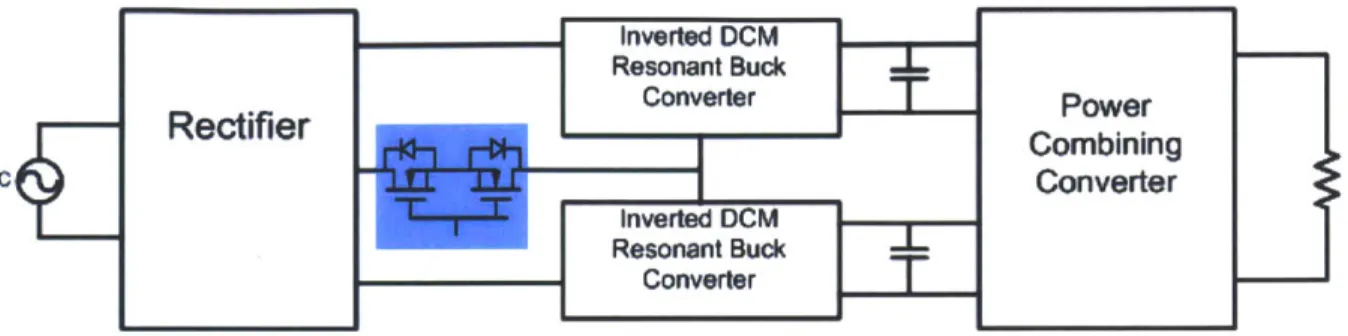
Our architecture is a variant of the two-stage standard PFC architecture that can more effectively handle the wide universal input range voltage while maintaining high-frequency and high efficiency. It has a reconfigurable input-stage, a high frequency power processing stage, and power combining, isolation and regulation stage. The approach is particularly suitable for utilizing conventional, high-efficiency high-density telecom "brick" converters as the isolation and transformation stage. In our work we principally focus on the PFC stage (with two outputs), and but do evaluate commercial telecom converters for use as the second stage.
Shown in Fig 2.9, our architecture of interest is closely related to the 2-stage PFC architecture. The input stage is comprised of a diode bridge rectifier and a frequency, low-loss switch. When the input voltage is low, the configuration switch turns on and the input stage functions like a full bridge rectifier. And, when the input voltage is high (>200V), the configuration switch turns off and the input stage functions like a voltage doubler. This allows the second stage to be designed for smaller current and voltage operating ranges which in turn
help us achieve switching frequency in the HF power stage.
The second stage "soft-switched high frequency power stage" comprises two inverted discontinuous-conduction-mode resonant buck converters, as shown in Fig 2.10. When the configuration switch is open, the two converters draw the same input current and deliver the same output current. And, when the switch is closed, each converter runs over half the line cycle only. The upper converter runs when the input voltage is positive, and the lower converter runs when the input voltage is negative. Consequently, the buck converters are rated for half the peak input current.
Isolation,
AC
C
]
PFC Stage
transformation,and regulation stage
Fig 2.8: Two-stage grid interface power converter with a first power-factor correction (PFC) stage, an
intermediate energy buffer, and a second isolation/transformation and regulation stage.
Inverted DCM Resonant Buck Converter Power RectifierCombining AC Converter Inverted DCM Resonant Buck Converter
T
Fig 2.9: represents the topology of our high-frequency PFC system. The first stage is comprised of a full
bridge rectifier and a configuration switch. When the input voltage is low, the switch allows the input stage to act as a voltage doubler. The two parallel buck converters function as a soft-switched HF power
stage. The power combining stage combines the output energy from the two buck converters.
This first part of the thesis is concerned with optimizing the performance of the inverted discontinuous-conduction-mode buck converter shown in Fig. 2.9. The converter operates from a
(80-186 V) input voltage range and outputs an average voltage of 72V with a current output up
to 8 Amps. And, the converter's output capacitors are required to buffer energies between 0.3 and 1 Joules. Table 2.6 below lists a summary of the current, voltage, and power requirements.
Note: The inverted resonant-transition buck converter operates in the same way as its non-inverted counterpart. The design chooses the inverted converter is because its active switch is referenced to a slowly moving node, while the non-inverted converter has its active switch is referenced to a "flying node" which restricts the maximum achievable frequency (and can degrade efficiency owing to the difficulty of driving the switch). However, using the inverted converters requires and extra stage to combine the two separate output energy.
in
i
Cn
v
-
out
*1LVL
L
+ V vgs ' -Vgs V& -4--VL Vint t ILfFig. 2.10a illustrates the topology and
components of an inverted resonant =
transition buck converter. This circuit works
as a high-frequency dc-dc conversion block 1 Fig. 2.10b Voltage and current waveforms in the two stage converter design with 81- of the resonant transition buck converter Illustrated in Fig 2.1Ob, the bottom curve represents the inductor current ripple, the blue curve represents the switch gate drive and the red curve represents the voltage across the switch. The buck converter operates with high current ripple in the inductor; the design achieves a high switching frequency by minimizing the transistor voltage stress and achieving zero-voltage switching. Although the topology only operates with "'ideal" ZVS soft switching over a 2:1 input voltage range (0.5 Vin < Vout < Vin), it still maintains high efficiency with a low ZVS over approximately a 3:1 input voltage range (-0.35 Vin < Vout < Vin). Moreover, the non-inverted resonant-conduction-mode buck converter has similar current and voltage characteristics, but does not have a ground-referenced switch.
Table 2.6 below shows a summary of the system and the single buck converter stage ratings we want to build:
Entire System Single buck converter
Input Voltage Range 85-265 Vrms 80-186 Vdc
Average Output Voltage 24 Vdc 72 Vdc
Average Output Power 240 Watts 573 Watts
Chapter 3
Twice Line Frequency Energy Buffering
This chapter covers a general study of the energy storage elements (capacitors and inductors), and the considerations taken into account when choosing the best devices - highest energy density -- to use for twice line frequency energy buffering. It also inspects the selection of the energy storage elements of a specific two stage PFC grid interface power converter.
3.1
Background and Motivation
Capacitors and Inductors are vital passive components in power electronic applications. Inductors are mainly used as magnetic energy storage elements while capacitors are used as electric energy storage elements. Other important uses include filtering, voltage and current stabilizing, and energy buffering. The topic of energy buffering is one that this document explores.
Often in power electronics, the size of a converter is dominated by passive components, namely the energy storage elements i.e. capacitors and inductors. There is an increasing demand for smaller, high efficiency, and high performance solutions for converters and power supplies. Since, energy storage requirements vary inversely with frequency. One way to decrease the size of needed passive components while still maintaining high performance is to operate at higher frequency.
That is why more and more power applications are utilizing higher frequencies to achieve, amongst others, higher energy density designs. We are interested in the energy buffering capabilities of capacitors, namely high energy density capacitors. This section is mainly
concerned with line frequency energy buffering. Energy buffering is independent of the converters operating frequency and depends only on line frequency.
In such applications and others, which require large capacitance values, electrolytic capacitors are mainly used. Electrolytic capacitors have bigger energy density than ceramic and film capacitors. They are often used as dc-link capacitors to reduce the ripple at dc output.
The goal is to find the capacitor with the smallest volume that satisfies our energy buffering and energy storage requirements to achieve a smaller overall system volume.
3.2 Architecture of interest
In many power electronics applications, especially multiple stage converters, there is a need for energy buffering. Our design of interest is a miniaturized two stage universal-input single-phase power-factor correction (PFC) converter which operates at high frequency. The first stage is a PFC stage and the second is a dc/dc isolation/transformation and regulation stage.
The two stages are connected by an intermediate energy buffering capacitor stage. High energy-density electrolytic capacitors can be used as buffering capacitors for interfacing between a single-phase ac source and a dc output load. Such applications our application of interest illustrated in Fig 3.1 below.
Isolation, +
Vin PFC Stage P Ste Transformation and Regulation Vout
- bui Stage
Energy Buffer
Fig 3.1 Two-stage grid interface power converter with a first power-factor correction (PFC) stage, an
intermediate energy buffer, and a second is a dc/dc isolation/transformation and regulation stage.
The converter shown in Figure 3.1 above operates from a universal-input single-phase ac
(85-265 Vrms and 50-60 Hz) to an isolated low-voltage dc output. While there are various
architectures to achieve such conversion, the two stage approach provides very small PFC stage size and enables the use of telecom "brick" converters as the second stage.
3.3
Capacitor Energy
To figure out the best capacitor, first we analyze the capacitors energy buffering capabilities and to do so first we look at the energy stored by the capacitor. From physics perspective, to figure out the amount of energy stored on a capacitor, we can look at a parallel plate capacitor. We calculate the work it would take to put charge on the two plates of the capacitor. Or, how much work it would take to move a charge element (AQ) from the negative plate to the positive plate. Knowing that voltage is equal to energy per unit charge the amount of work it takes to move (AQ) from one plate to the other is:
AW = Fd = AQEd = VAQ (3.1)
Where F is the force needed to move AQ, d is the distance between the two plates, E is the electric field, and V is the capacitor voltage. Now we add up the work done to charge up the capacitor to
Q.
Energy (E) =f dW = VdQ = dQ = (3.2)
f 0 oCbuffer 2 Cbuffer
If we use the fact that (dQ = CdV) in the above equation, we get that the amount of energy
stored on a capacitor in terms of voltage and capacitance:
CbufferV 2
Energy (E) = 2 (3.3)
It is often the case in applications that we charge and discharge only a fraction of the energy stored on the capacitor. For simplicity, we look at a sinusoidal capacitor voltage waveform. The energy we need to buffer in that case depends on the maximum voltage (Vmax) and minimum voltage (Vmin) on the capacitor.
Vmax
. ... ... ... ...... ... ... ... ... ... ... ... ... ... ... ... ... ... ... ... ...
ri mv - --- --- ... ... ... _ --- --- --- --- ---
---
Vnom-Fig 3.2 Capacitor voltage sinusoidal waveform
The equation for the buffered energy then becomes:
1 21 2_1 ( ax -m 2) ()
Ebuffer = -Cu~rmax 2- -CufferVminz = ChbuferV Va2
3.4
Capacitor Energy Buffering
In Fig 3.1, repeated below, the capacitor C buffer provides twice-line-frequency energy
buffering and energy for "holdup" to support the second stage operation over a temporary input line-voltage outage.
iline-p-Isolation,
Viine(t) AC PFC + transformation
Front equCtonfer and Regulation e
End Cstage
Fig 3.4 Two-stage grid interface power converter. The first stage is a power-factor correction (PFC)
circuit, followed by an intermediate energy buffer. The second stage is a dc/dc converter that provides isolation/transformation and regulation stage.
Since we are considering electrolytic capacitors to achieve a high energy density design, we analyze three possible constraints to achieve minimum capacitor size:
1- Energy density constrained by design allowed ripple.
2- Energy density constrained by capacitor RMS limit.
3.4.1 Energy Density Constrained by Allowed Ripple
The amount of energy and capacitance needed to limit the voltage ripple in vc to within an acceptable range. The range is constrained by the operation of the PFC first stage and/or the second stage. The allowable ripple value is chosen by the designer.
The characteristics and shape of the capacitor voltage ripple is depends upon the PFC and second stage. However, if we make the simplifying assumption that the mean voltage of the waveform is half way between the peaks (as for sinusoidal or triangular ripple). We can use the "ripple ratio" Rc to characterize the waveform:
Vc,max -Vc,nom Vc,min -- -- -- Vc,nom(1 + Rc) ---- Vc,nom(l - Rc) ... ... .. ... .. .... ... ...
..
...
...
....-
.
...
...
... .... .....I .... ... .... .---- --- --- ----- -- -- -- - -TT T T U- h- -7- 8- 9 0 T uneT line 4 2Fig 3.5 Capacitor sinusoidal voltage ripple
I
Where,
R = Vc,max - Vc,min - Vc,max 1 (35)
2
Vc,nom Vc,nom
If we state that there is an allowed limit on ripple ratio (for converter design and operation purposes) we can express the energy buffered in a cycle as:
Ebuffer = Cbuffer (vc,max 2 - Vc,min2)
1
= CbufferVc,nom 2((1 + Rc)2 - (1 - Rc)2)
-CbuffVerc,nom 2((1 + Rc)2
_ (1 - Rc)2)
= 2RcCbufferVc,nom2
1 4R~
Ebuffer = g CbufferVc,max2 (1 +
c)2 (3.6)
If Vc,max is the capacitors rated voltage, the peak energy storage capability of the capacitor is:
1 1
Ec,pk = CbufferVc,max2 = CbufferVrated2 (3.7)
Hence, by substituting (3.7) into (3.6) we can write the capacitor buffered energy as:
Ebuffer = Ec,pk (1 (1+ Rc)4R 22 (3.8)
We can also find the usable energy density as:
Ebuffer
Volume
Ec,pk 4Rc
Volume (1 + Rc )2 (3.9)
Where 4RC is the fraction of peak energy storage we can access at ripple ratio Rc. So if (1+RC)2
we know the peak energy density of a capacitor, we can find the usable energy density as constrained by ripple ratio.
The plot below shows the usable energy density for 5 different ripple ratio values against the rated voltage of all electrolytic capacitors listed on digikey.com (the website for the electronics supplier DigiKey). The data was downloaded on Feb 2015.
Usable Energy Density vs Rated Voltage for specific ripple 18 -+ Rc=20% 16 - + Rc=15% Rc=10% 14 - Rc=5% * Rc=1% 10 -Eo
1
6 -2+
0 U 100 200 300 400 500 600 700 Rated Voltage (V)Fig 3.6 Usable energy density vs. rated voltage for available electrolytic capacitors for several ripple ratio values
We notice from Fig 3.6 that the higher ripple ratio gives us higher accessible energy (and hence higher energy density). We also notice that the highest energy density capacitors are the 400 V capacitors. (This may in part be because 400 V is an extremely common storage voltage for twice-line-frequency energy in grid-interface power supplies, and hence highly-optimized capacitors are available at that voltage rating.)
Furthermore, Fig 3.7 applies equation (3.10) to show the usable energy normalized by peak capacitor energy for different ripple ratio values:
Ebuffer 4RC
(3.10)
Ec,pk (1 + Rc)2
Usable Energy/Peak Energy vs Ripple Ratio
0.9 0.8 -0.7 -0.6 0.5 -w 0.4 - 0.3-0.2 - 0.1-0 0.1 0.2 0.3 04 05 0.6 0.7 0.6 0 9 1 Ripple Ratio
3.4.2 Energy Density Constrained by RMS Current Limits
A second factor that may constrain the usable energy density of the capacitor is RMS current limits (which are ultimately governed by the thermal constraints of the capacitor). Before analyzing the RMS current constraint and what it means to a capacitors energy buffering capabilities. First we need to understand the meaning of the RMS ratings and why they are important.
The average current which flows in and the average voltage across AC circuit elements with sinusoidal excitation is zero, as shown below.
1 7T 1
rcos(wt)]T
1 peaIavg = Ipeaksin(w) dt = -Iveak - = [cos(27r) - cos(O)] = 0
T 0 T W 10 T w
However, for joule heating of the capacitor (e.g., owing to parasitic resistance) we are concerned with average power dissipation in the parasitic resistance. This average power dissipation is related to the average of the square of the current times the parasitic resistance. Thus, despite the fact that the average current is zero, what we care about as regards parasitic heating is the square-root of the mean-square current. (The rms or root-mean-square current is the dc current that would generate the same dissipation in the same parasitic resistance as the original current.) That is why we use the RMS values of current and voltage when dealing with AC circuits. Furthermore, multi-meters output RMS values for current and voltage rather than peak values. The RMS value is the square root of the arithmetic mean of the squares of the values or waveform that define a function.
When currents is defined by a set of n values 1, I2, 13, ..., I,} then
I2 +22 +I2 + ..-- + I"2
IRMS
-(3.11)
IRMS = 2 1 T I(t)2dt (3.12)
IRMS is an important concept which is usually overlooked when using capacitors. If not considered properly, excess current may cause the capacitor to overheat and fail. Hence, IRMS
constrains the amount of energy a capacitor can buffer.
For our architecture, the RMS current limit constraint depends upon the current waveforms from the PFC stage and the current drawn by the second stage (e.g. for constant power to output). The current from the PFC stage likewise depends on the power factor and line voltage, as does the energy buffering requirement.
The simplest case to calculate, which also represents the best case, is to assume that the energy buffering capacitor charges and discharges at a constant current (charging for 1/4 of the
line cycle and discharging for /4 of the line cycle). This represents the maximum usable energy
from a capacitor within a given RMS current limit; all other situations will be worse (having a lower Av, for a given RMS value). Fig 3.8 shows the waveforms of this scenario.
Square Current waveform
I I T m
Triangular \/oltage waveform
-c,nom ~- - - ~ ... .. . ...-IO 20 25 3 3 5 Time T line Tie 4 2
Note that for the square wave the instantaneous charge and discharge current is the RMS current. Also, the plotted capacitor voltage ripple neglects the effects of ESR on the voltage ripple waveform.
If we assume that the capacitor charges and discharges at its RMS current limit:
Avc = Ic,rmsTuine
4Cbuffer (3.13)
1
Ebuf fer = g Cbuf ferVc,max 1 2 Cbuffer (Vc,max 2 Avc ) 12 = Cbuffervc,maxAVc - CbufferArc 2 = CbufferAVc(Vc,max AvC 2 ) (3.15)
Ebuffer = CbufferVcnomAVc = VcnomlrmsTine
4 (3.16)
From Fig 3.8 if we set Vc,max = vc,rated and substitute in for (3.13), we get:
Vc,nom = Vc,rated - = c,rated - crmsTie
2 4Cbuffer
(3.17)
Now we can calculate the capacitors buffered energy:
J'c,rms iine Ebuffer - 4
(Vc,rated
4 ~rmsTline 8Couffer) (3.18)Note that we can do related calculations for different charge and discharge waveforms to relate ic,rms
toAvc-For our application, we would like to identify the best capacitor in terms of usable energy and usable energy density. Fig 3.9 below uses equation (3.16) to show the energy density vs. Hence,
rated voltage constrained by RMS current capability of the available electrolytic capacitors in the market.
The output power is 120W and the frequency is 100 Hz. The capacitor data was downloaded from digikey.com on Feb 2015. Note, the plots show the best 522 capacitors. The plots below use the rated voltage instead of the nominal. Similar trends are noticed when using nominal voltage.
The highest energy density capacitors constrained by their RMS current limit are again the 400V capacitors. One can use capacitors even down to 80 V, paying for a penalty of less than a factor of two in energy density. Tables 3.1 and 3.2 below list the highest energy capacitors constrained by RMS current limit.
2
0 W
0.5-50
Usable Energy Density vs Rated Voltage
I
4 +j
100 4 *I
t
I
I
150 200 250 300 350 Rated Voltage (MI
g
4I
400 450 500Fig 3.9 Usable energy density taking into consideration RMS current limits and triangular voltage waveforms
2.5 r
Manufacturer Part Number UCY2H I 50MHDiTO 'CY2H I15OMH[D 380LX470M500H012 450QX4! M FFCliX45 450QXW39MEFC1OX40 C'W2 N N) UCY2G6 MHD UCS2C22M H D1TO UC(2G'2MDTN RMS Height Diameter Current (In) 1.043 1 .043 0.984 1.85 1 654 634 1 (64 (In) 0.49 0 86 0.39 0,39") 49) (A) '.6 4 0.44 - I Voltage Rating (V) 500 450 450 400 Of0 Capacitance (uF) Usable Energy (J) 15 0.275 I f Usable Energy Density (J/1n3) L386846 47 47 39 o. / 0.72 2 098682 %;i371
Table 3.1 lists the highest energy density capacitors constrained by RMS current limit available at 400V to 500V.
The RMS current is calculated at 100 Hz (twice-line frequency)
Manufacturer Part Height Diameter RMS Voltage Capacitance Usable Usable Energy Number
ICS2D680M HD TO C2 ) 6 807DU3TQ
UC1 2 b2AH 9TO
UCY2C82OMHD3TO U CY2C82MHD3T() FlEt- E2C 70 E1F) - 147 F2 C470t EK ZN1 I1 1Li',i 7 E KL Z 3 LI 39B ( 714f 35 EKZN800ELL221MJ25S EKZN800ELL820MH2OD EIKZN800ELL27OMF1I D D CM'1C a 03 L 7 5 B C2 BDCMC 3U752 r1 (In) (In)2 U 846 0 492 1.846 0.846 0. 846 0.492 0.492 0 4C 1) 94 /i <4 53 (1. 0 758 1.043 0.394 0,846 0.31.5. 0.492 0.248 5.687 1.3'75 41 2 Current Rating (A) (V) Ot 6 4 5 0.64 0.64 0.98 0. 28 0.816 0.148 1. 100 80 80 80 (uF) 82 82 , 33 220 8.. 27 $220 -7 j)' I 0.22 0.256 0 2, I 0. 0 062 0.162 0.0832 0.0296 2) 0,f7
Table 3.2 lists the highest energy density capacitors constrained by RMS current limit available at 75V
to 20GV. The RMS current is calculated at 100 Hz (twice-line frequency)
Energy (J) Density (J/In3)
1.591657 1, 59 16 7, S!3;6 1.273938 1.261949 1 .24547 02 2379
3.4.3 Hold up time requirement
Moreover, when designing systems for applications such as DC/DC converters in telecom and Off-line power supplies, designers are faced with the topic of hold-up requirement. In such applications, the design must be able to continue operating for a set time (Tholdup) after the input energy source turns off at a specified converter load (e.g., one line cycle at full load). During this time the energy is taken from the buffering capacitor of the converter.
Hence, a third factor that might constrain capacitor size is the holdup time requirement. It is assumed for this case that the AC line voltage goes away for some duration Th"Odup and that converter is required to support an output power Poholdup during this time. Moreover it is
assumed that the buffer capacitor may discharge down to vc,ho lmin during this time. The
waveforms are illustrated in Fig 3.10 below.
Capacitor Voltage vs Time
Vc,max Vc,nom Vcmin Vc,holdmin T line Tine 4 2 Time
Fig 3.10 illustrates the capacitor voltage vs time under holdup requirement
Fig 3.10 above illustrates the capacitor voltage under normal operation where the voltage ripples around the nominal voltage and under holdup operation where the voltage drops down to the minimum operating voltage of the second stage.