HAL Id: hal-03009678
https://hal.uca.fr/hal-03009678
Submitted on 17 Nov 2020
HAL is a multi-disciplinary open access archive for the deposit and dissemination of sci-entific research documents, whether they are pub-lished or not. The documents may come from teaching and research institutions in France or abroad, or from public or private research centers.
L’archive ouverte pluridisciplinaire HAL, est destinée au dépôt et à la diffusion de documents scientifiques de niveau recherche, publiés ou non, émanant des établissements d’enseignement et de recherche français ou étrangers, des laboratoires publics ou privés.
Limitation of simple np-n tunnel junction based LEDs
grown by metal-organic vapor phase epitaxy
Y Robin, Q Bournet, G Avit, M Pristovsek, Y André, A Trassoudaine, H
Amano
To cite this version:
Y Robin, Q Bournet, G Avit, M Pristovsek, Y André, et al.. Limitation of simple np-n tunnel junction based LEDs grown by metal-organic vapor phase epitaxy. Semiconductor Science and Technology, IOP Publishing, 2020, 35 (11), pp.115005. �10.1088/1361-6641/abad73�. �hal-03009678�
Limitation of simple np-n tunnel junction based LEDs grown by MOVPE
Y. Robin1,*, Q. Bournet2, G. Avit1, M. Pristovsek1, Y. André3, A. Trassoudaine3 and H. Amano1
1 Institute of Materials and Systems for Sustainability (IMaSS), Nagoya University, Japan 2 Polytech Clermont-Ferrand, Université Clermont Auvergne, France
3 Institut Pascal, Université Clermont Auvergne, CNRS, SIGMA Clermont, F-63000 Clermont-Ferrand, France ---
* Yoann.robin@crhea.cnrs.fr
We show evidence that tunnel junctions (TJs) in GaN grown by metal-organic vapor phase epitaxy are dominated by defect level-assisted tunneling. This is in contrast with the common belief that highly doped layers (> 1020 cm-3) are required to narrow the TJ space charge region and promote the band-to-band
tunneling. Our conclusion stems from the study and the review of the major doping limitations of carefully optimized p++ and n++ layers. The secondary ions mass spectroscopy profiles of GaN based TJ LEDs show
a strong oxygen concentration located close to the p++/n++ interface, typical for three dimensional growth.
In addition, considering the doping limitation asymmetry and Mg carry-over, our simulations indicate a depletion region of more than 10 nm which is buried in a rough and defective n++ layer. However, decent
electrical characteristic of the studied TJ based LEDs are obtained, with a low penalty voltage of 1.1 V and a specific differential resistance of about 10-2 W.cm2 at 20 mA. This indicates that common TJ could
be greatly optimized by using a moderate doping (~1019 cm-3) while intentionally introducing local defects
within the TJ.
I. INTRODUCTION
Realization of high-quality p-n homojunction based on wide bandgap semiconductors is challenging due to doping asymmetry problems [1]. GaN, with a bandgap of about 3.4 eV, does not deviate the rule. While doping n-type is rather simple, achieving decent p-type layers is not straightforward [2,3].
Intentional n-type doping of GaN is traditionally realized by substituting gallium by silicon, which allows to reach electron concentration up to 1019 cm-3. However, at higher doping levels, Si
doped GaN layers tend to roughen or crack under tensile stress [4,5]. Recently, germanium, whose size is comparable to gallium, has been studied as alternative dopant to cover the 1019-1020 cm-3 range
[6-8]. Oxygen on N-site is an efficient n-type donor, although only few reports exist on intentional oxygen doping [9-11]. N-type doping of GaN by
other chalcogens (sulfur, selenium…) substituting the nitrogen site is little investigated. However, their huge size difference to nitrogen does not bode well for achieving high doping levels and the relatively low vapor pressures of these solid easily cause strong carry-over [12,13].
For p-doped GaN, there are even less suitable acceptors. Zinc, a standard dopant in other III-V materials, is still a relatively deep acceptor in GaN (Ea~300-400 meV) [14]. Carbon exhibits an
amphoteric behavior and beryllium is a shallow acceptor (Ea~100-140 meV) but suffers from
severe self-compensation [15-18]. Other unsuccessful attempts were made using calcium, cadmium and mercury [19]. In the end, magnesium is the only dopant that allows a decent p-type conduction after an activation. Unfortunately, the maximum hole concentration barely reaches 1018 cm-3 due to the large ionization energy
magnesium can be incorporated before onset of compensating defects [20-22].
Recently, tunnel junctions (TJs) have gained interest in nitrides. Indeed, such TJs reduce optical loss in UV-LEDs, alleviate non-equilibrium hole injection and allow a better current spreading in higher mobility n-type layers [23-24]. Such properties pave the way for inter-cavity contact in vertical cavity surface emitting lasers (VCSELs) and simpler vertical integration of tricolor micro-LEDs [25-28]. Esaki junctions typically require both low or moderate bandgap materials and doping levels around 1020 cm-3 that is out of reach
for GaN [29]. Nevertheless, GaN based TJ based LEDs reported unexpectedly low penalty voltages [30-36]. The common explanation widely found in the literature considers that over-doping the n- and p-type layers, along with the insertion of a thin InGaN layer, reduces the width of the space charge region of the TJ and enhances band-to-band tunneling. The defects assistance is mostly considered as a minor or negligible contribution. In this paper, we show evidence that midgap defect level-assisted tunneling is the main mechanism responsible of the surprisingly high efficiency of TJ grown by metal-organic vapor phase epitaxy (MOVPE). In a preliminary study, we first summarize the general crystal properties of simple p- and n-GaN layers depending on growth conditions. We highlight the morphology changes, the secondary ion mass spectroscopy (SIMS) profiles of dopants and impurities, and the defects typically generated upon heavy doping in TJs. In a secondary part, we compare the electrical behavior of simple np-n structures and corresponding TJ based LEDs grown without using InGaN interlayer. Based on those findings and further band diagram simulation, we conclude that Poole-Frenkel effect is the main tunneling process involved in such TJs while band-to-band tunneling (Fowler-Nordheim) is much less likely given the large band gaps and relatively low carrier concentrations. Finally, we
discuss TJs found in the literature in the light of our observations and results.
II. EXPERIMENTAL DETAILS
All the samples were prepared in a 3x2” EpiQuest vertical showerhead MOVPE reactor. For Si and Mg doping, pure H2 was used as carrier gas. Both
Mg:GaN and Si:GaN layers were grown using a V/III ratio of 7200, at a pressure of 150 Torr and at temperatures ranging from 975 to 1100°C with a growth rate of about 500 nm/h. Bisethylcyclopentadienyl-magnesium (EtCp2Mg),
tetramethyl-silane (TMSi), trimethyl-gallium (TMG) and ammonia (NH3) were used as
metal-organic precursors. For the growth of the quantum wells (QWs), the carrier gas was switched to pure N2 and triethyl-gallium (TEGa) and
trimethyl-indium (TMIn) were used as precursors.
Electrical characterizations were performed by Hall effect measurements (HEM) in Van-der-Pauw geometry. For Si doping levels below 1019 cm-3
Hall effect measurements and secondary ion mass spectroscopy (SIMS) concentrations agreed. Above that limit, the dopant concentration was measured by SIMS or given as extrapolation of our calibration. Photoluminescence (PL) was performed at room temperature (RT) using a He-Cd laser (lex=325 nm, P=1 mW). For the activation
of the simple Mg-GaN layers, the samples were annealed at 700°C for 5 minutes under N2. Surface
morphologies were investigated by a Nanocute Hitachi atomic force microscope (AFM) working in tapping mode and by Nomarski optical microscopy (OM).
TJ based LED structures were processed by standard photolithography. L-shape mesa of 0.0675 mm2 were prepared using Cl2 dry etching.
Then, the devices were annealed for 30 min at 750°C in N2 ambient in order to activate the buried
p-GaN layers (notice it is different from the annealing conditions used to activate simple p-GaN
layers). Finally, Ti/Al electrodes were simultaneously deposited by e-beam evaporation on both n-GaN terminals and annealed 5 min at 625°C in pure N2. For the reference LED, p-GaN
top layer was contacted by a Ni/Au electrode annealed 10 min in air at 500°C.
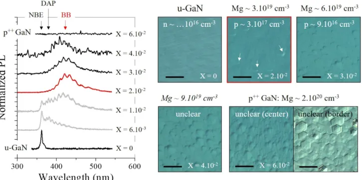
III. RESULTS AND DISCUSSION Fig. 1 summarizes the morphological, optical and electrical properties of 500 nm thick Mg doped GaN layers grown at various Mg/Ga ratios, which is in line with current literature. The near band edge (NBE) emission of the PL slowly decreases and a characteristic donor-acceptor pair (DAP) related signal appears while increasing the Mg content [37].
A strong blue-band (BB) dominates the PL spectrum when the hole concentration reaches its maximum around few 1017 cm-3 at RT,
corresponding to a Mg concentration of few 1019
cm-3 [38]. Further increase of the Mg content leads
to the apparition of various compensating defects and pyramidal inversion domains (IDs) [22]. Simultaneously, the doping level drastically decreases and the p-GaN layers become resistive. At a Mg concentration of a few 1020 cm-3 - which
is the doping level typically required for TJs - the surface is rough and decorated with large hexagonal N-polar hillocks likely induced by the formation of Mg3N2 sub-structures [39,40]. A high
density of defects is indicated by the absence of any PL signal.
FIG. 1. Normalized PL emission spectra and associated optical microscope pictures of post-annealed GaN grown at 975°C at various X = Mg/Ga ratio. The red PL spectrum highlights the highest doping level achieved. The OM pictures related to the
grey PL spectra are omitted. The scale bar corresponds to 50 µm.
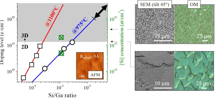
Fig. 2 shows a similar study on 500 nm thick (crack-free) Si doped GaN layers grown at various Si/Ga ratio using TMSi. This Si precursor mostly decomposes above 1000°C, which is different from the common silane precursor, hence calibration was performed at two temperatures [41]. The
electron concentration increases with the Si/Ga ratio both for growth temperature of 975 and 1100°C. At Si concentration exceeding 1.5×1019 cm-3, the surfaces show large scale-like
islands of different heights separated by pitted boundaries. Further increase of the Si level leads to
extremely rough surfaces characterized by larger pits and smaller grains, similar to previous reports [5,42]. Under typical MOVPE growth conditions and for a concentration higher than 1019 cm-3, Si
acts as an anti-surfactant. It was suspected to locally form Si-Ga-N substructures, which initiate a SiNx nano-masking that promotes 3D growth
[43,44]. According to high resolution transmission electron microscopy, the actual SiNx masking is
actually a SiGaN3 monolayer that inhibits Ga
nucleation and thus causing islands growth in uncovered areas [45]. Therefore, at the doping levels used for TJ application, i.e. above 1020 cm-3,
Si behaves as an anti-surfactant rather than a dopant, as it is incorporated inactively in SiGaN3.
We observed that the 2D-3D transition always happens around a doping level of 1019 cm-3
regardless the growth temperature. Thus, the 2D-3D transition is driven by the actual Si concentration on the surface and not by the surface kinetics of Ga or the Si precursor we used. The
different Si/Ga ratio is due to the decomposition kinetics of the TMSi, whose decomposition temperature is estimated to be around 1000°C [41]. In other words, the supply of active Si, i.e. the effective Si/Ga ratio in the gas phase, depends with TMSi on the growth temperature. SiH4, a more
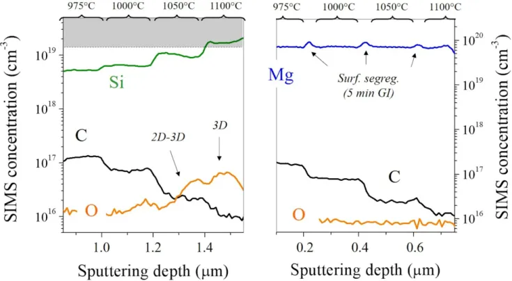
common precursor, does not present such disadvantage since it is fully decomposed around 700°C, and thus usually no temperature dependence of the roughening has been reported. Fig. 3 (left) shows the SIMS profiles of Si doped GaN layers grown successively on the same template at four different temperatures without varying the other growth parameters, i.e. keeping the NH3, TMGa, TMSi flows constant. Fig. 3
(right) shows the similar SIMS analysis performed on Mg-doped GaN grown at four different temperatures on the previous Si-GaN stack. Unlike TMSi, the EtCp2Mg decomposition and further Mg
incorporation is stable over temperatures ranging
FIG. 2. Doping levels measured by HEM (open black symbols) and dopant concentration (crossed green symbols) measured by SIMS of Si:GaN layers grown at 1100°C (square) and 975°C (circle) for different Si/Ga ratio. The thick left-right arrow
indicates the conditions typically required for the growth of TJ. Three kind of surface morphology can be observed depending on the doping concentration: a very smooth surface below 1019cm-3 (white area / AFM picture inset), a highly textured surface between 1.1019 and 2.1019cm-3 (dashed line / right bottom SEM and OM pictures) and finally a very rough
FIG. 3. SIMS analysis of n-GaN (left) and p-GaN (right) layers grown on the same template but at different temperatures. The O signal increases of one order of magnitude when the Si level is higher than 1019/cm3, i.e. when the growth mode changes from 2D to 3D. The Mg incorporation is constant over the full temperature range between 975 and 1100°C but Mg
tends to accumulate on the surface during each growth interruption.
from 975 to 1100°C. Mg piled up at the surfaces during the 5 min growth interruptions (GI) used to ramp up and stabilize the temperature between each step, which indicates we doped below the absolute solubility limit. Both for Si:GaN and Mg:GaN, the carbon level increases from 1016 to 1017 cm-3 when
the growth temperature decreases from 1100 to 975°C. This is commonly attributed to the lower decomposition rate of NH3 and less active H
readily available to react and etch away hydrocarbons species present on the surface and is also observed at similar level in undoped layers. Such levels do not significantly affect the GaN conductivity. Interestingly, the O signal is very
different for both layers. While the background level remains below 1016 cm-3 throughout the
p-GaN growth, the O concentration increases of one order of magnitude when the n-GaN doping level reaches about 1019 cm-3. Conversely, once the Si
level decreases below 1019 cm-3, the O
concentration slowly returns to the background level. Since 3D growth starts above 1019 cm-3 as
mentioned previously, and 3D growth generates additional semi- and non-polar facets which are usually prone to higher O incorporation, the O signal correlates with the 2D-3D growth transition [46].
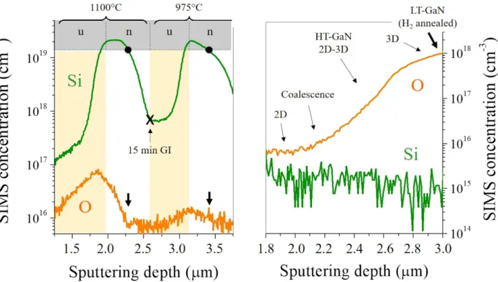
FIG. 4. SIMS analysis of different n-GaN (left) and u-GaN (right) layers. Each time, an increase of the O level is observed when the 3D growth mode is triggered (thick arrows and dots), either by a Si concentration higher than 1019 cm-3 or by a H2 annealing of a LT buffer layer. Further GaN overgrowth of the rough surface with proper conditions leads to coalescence and
the O level simultaneously decreases to below 1016 cm-3 in both cases.
Fig. 4 presents two additional evidences for correlation of the O level with 3D growth, triggered with and without SiNx nanomasking. For the first
sample, 600 nm n-GaN is grown at 975°C with a linear increase of the Si concentration up to several 1019 cm-3, followed by a 600 nm u-GaN to recover
a smooth surface. After a 15 min growth interruption, where no Si surface segregation is observed, the same sequence is repeated at 1100°C. It is worth noting that the O concentration increases as soon as the 3D growth is triggered by the SiNx
nanomasking (black dots and arrows on Fig. 4
(left)). Conversely, the O level slowly decreases
upon u-GaN overgrowth which again smooths the surface. The second sample shows a similar behavior (Fig. 4 (right)) during a u-GaN template growth on sapphire. Here, intentionally, 3D islands are obtained by annealing a nucleation layer deposited at low temperature (LT). At this point, the O level is around 1018 cm-3. Further regrowth of
the 3D nuclei at high temperature (HT) smooths the surface. Since this means that the semipolar facets are vanishing, the O concentration also decreases until it reaches its background level of about 1016 cm-3 for O incorporation on a flat (0001)
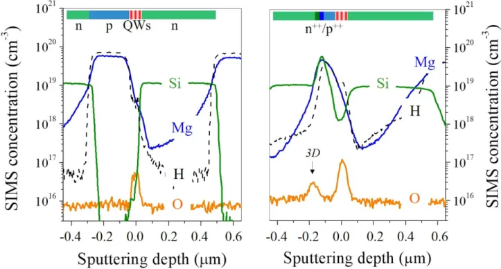
FIG. 5. SIMS analysis of the np-n (left) and TJ (right) based LEDs. In the p-type layers, the Mg is still passivated, i.e. [Mg]~[H], since the structures have not been annealed at this stage. Note the O peak and the Mg tail buried in the n++ side of
the TJ. The x-axis origin has been set at the QWs position for better comparison.
Fig. 1, 2, 3 and 4 indicate a rather low doping limit on both Si:GaN and Mg:GaN, which would be theoretically unsuitable for a TJ. However, driven by many successful reports found in the literature, we compared the SIMS profile of a “np-n” LED (no n++/p++ layers at the p-n junction) and one with
n++/p++ layers “TJ based” LED. Fig. 5 (left) shows the results of the “np-n” LED structure featuring the highest doping level for smooth surfaces as determined from Fig. 1 and 2 (~1019 and
few 1019 cm-3 for Si and Mg respectively). The O
level exhibits a peak around the QWs position, most likely due to the residual O found in the N2
carrier gas required for the InGaN growth (n- and p-GaN are grown under pure H2 carrier gas, which
is easier to purify and present lower contamination levels). Since Mg has a strong carry-over into subsequent layers, it is also incorporated in the Si:GaN top layer [47-49]. Even though Mg decreases drastically, the first ten nanometers of intended n-type layer is rather p-type since there is
still a higher Mg than Si concentration. In conclusion, the electrical interface, i.e. the dopants profiles of the maximum doped np top junction are not as well defined as intended. The right side of fig. 5 shows the same structure but with a 15 nm/15 nm n++/p++ layers typical for TJ inserted
between the n- and p-GaN top layers. The Si and Mg levels were aimed to be around 2×10²⁰ and
1×1020 cm-3 respectively. The SIMS analysis in Fig.
5 (right) shows that an additional O peak appears in the n++ region, indicating a rough interface due
to 3D growth. Unfortunately, the SIMS profiles lack depth resolution, i.e. the concentration of the different elements is averaged over a larger volume, depending on how flat the sputter crater is at this position. This underestimates the concentration in these layers. Still, when reaching appropriate Si:GaN growth conditions, the rough surface can be smoothened by a proper overgrowth. Thus, as expected from Fig. 2, the 15 nm thin n++ layer has
discontinuous. It is worth noting the electrical interface and the metallurgical are not located at the same position. Due to the strong Mg carry-overs, the electrical interface is buried in the n-side of the junction, around 10 nm away from the rough metallurgical interface. In short, both interfaces are not the abrupt interfaces typically assumed for TJs. At this point, one has to remember that it is not straightforward to activate buried p-GaN layer due to the impossible vertical diffusion of H through the n-type top layer (note the LED structures presented in Fig. 5 were not activated at this stage as it can be seen by the Mg/H ratio close to 1). Therefore, we remind that the TJ LEDs had to be annealed 30 min at 750°C in N2 for further
electrical investigations. This has been done right after the mesas etching, allowing the H to out-diffuse laterally through the sidewalls. Such Mg activation is mostly limited by the size of the mesas since the diffusion length of the H seems proportional to the square root of the annealing time [33]. In our case, we considered the most favorable situation for the next discussion, i.e. we assumed the p-type layer of our L-shape TJ LED fully activated since the expected H diffusion length (~ 100 µm) is larger than half the typical dimension of our mesas.
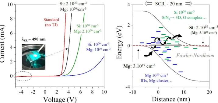
Fig. 6 (left) compares the IV characteristics of three TJ based LEDs with different p++ and n++ doping
levels. The reference is a standard cyan LED emitting at a wavelength of 490 nm (red curve). In good agreement with the results found in the literature, the TJ based LEDs show typical LED behavior and emit light once both Mg and Si expected levels reach about 1020 cm-3 [31]. A
further increase of either dopant concentration leads to a significantly decrease of the penalty voltage. Si seems more efficient than Mg at lowering the junction barrier, as previously observed by Kaga et al. [32]. Eventually, for Mg and Si levels of 1020 and 2×1020 cm-3 respectively,
the TJ based LED penalty voltage is reduced to as
low as 1.1 V with a specific differential resistance of about 10-2 W.cm2 at 20 mA. These values are
surprisingly low considering the present structure does not involve any (p-)InGaN interlayer that is often introduced between the p++ and n++ layers to
reduce the nominal tunnel barrier height and facilitate the tunneling process [29,50]. It is worth noting at these doping values, the TJ starts to leak at negative bias (Fig 6. dashed circle). A further increase of the Mg and Si levels led to an electrical shortcut of the junction, i.e. the I-V analysis become characteristic of a pure resistor.
Based on the rather poor morphological, crystalline, and electric properties of the overdoped doped n++-
and p++-GaN layers in TJs as shown in the previous
sections, the results of Fig. 6 (left) seriously challenge a pure tunneling mechanism for the following reasons:
i) Assuming no Mg-H passivation (100% H free), which is the most favorable case, the maximum free carrier density achievable in the p++ and n++ side of the junction is limited
around 3×10¹⁹ and 2×1019 cm-3 respectively.
Therefore, the space charge region (SCR) spreads over a distance of 20 nm which is not compatible with a Fowler-Nordheim emission, given the large bandgap of GaN. If one further considers that the buried Mg:GaN layers might not be fully activated, the SCR is even larger and the tunneling process even less likely.
ii) The Mg carry-over causes fairly high amount of active, i.e. not passivated, Mg (>1019 cm-3)
to be incorporated in the n++ side. This leads to
a significant compensation of the free electron density, especially at the vicinity of the interface, which widens the SCR and so further reduces the electric field across the junction.
iii) Due to the effective doping asymmetry p++>n++ deduced from i) and ii), the SCR is
junction is characterized by a low structural quality and a high O contamination at grain boundaries inherited from a SiNx induced 3D
growth. Worse, the presence of Mg likely induces additional defects such as IDs, or Mg-O and Mg-Si complexes. Thus, the field of the SCR is strongly affected by (various) deep centers that prevent the free carriers to directly tunnel from one band to the other one, and could even pin the Fermi level at their midgap states.
iv) Any attempt to increase the Mg and Si concentrations up to 1020 cm-3 exacerbates the
problems discussed in points ii) and iii) even though the penalty voltage decreases and the TJ starts to leak.
These considerations imply that a defect level-assisted tunneling, i.e. Poole-Frenkel emission, is the main mechanism responsible for the TJs in GaN [51]. The band diagram of such TJ and the proposed tunneling mechanisms are sketched in Fig. 6 (right). For this band alignment, the most favorable situation has been considered in the p++
type layer: p = Na-Nd ≈ Mg (i.e. we assumed all the
Mg atoms are in substitution of Ga, fully activated by the electric field and free of H passivation). For the n++ type layer, we took a donor concentration of
2.1019 cm-3 and we included a Mg carry over
decreasing from 3.1019 cm-3 at the metallurgical
interface down to 5.1018cm-3 at 50 nm (as observed
from Fig. 5 and references [47-49]). Again, this corresponds to an ideal case, the most favorable for a TJ “free of defects”. In a more realistic case, one would have to consider the whole 10 nm p++ layer
mostly self-compensated (quasi-insulating) and a larger SCR buried in the n-side characterized by various crystal defects such as Mg clusters, IDs, SiNx nanomasking, O complex, etc. Finally,
instead of the low probability of direct band to band tunneling on such a long distance, the carriers could tunnel through defect states. So even a less abrupt band transition can still allow relatively efficient tunneling, because the tunnel current is then rather limited by the distance, both in space and energy, between the intermediate states. More states could sustain higher tunnel currents. It is worth pointing out a similar mechanism should occur with AlGaN. Here the problems are even worse since the larger gap would require even higher dopant concentrations and associated issues. In addition, at higher levels, the Si forms DX centers in AlGaN [52]. Hence, overdoping would lead to more midgap states. This explains the recently reported relatively high conductivity of AlGaN TJ in deep UV LEDs [21].
FIG. 6. I-V characteristics of standard and TJ based LEDs with different p++ and n++ doping levels. The dashed circle highlights the current leakage at negative bias for the most heavily doped TJ (left). Band diagram of unbiased TJ assuming that the p and n doping levels saturate at 3×10¹⁹ and 2×1019 cm-3 respectively, and considering the carry-over of Mg (right).
The curved black arrows sketch the defect level-assisted tunneling (Poole-Frenkel emission). The straight grey arrow represents a pure tunneling (Fowler-Nordheim emission). Note the position of the defect levels is arbitrary.
It is worth pointing out our explanation contrasts within the dominant thinking where defects only play a secondary or even negligible role. Therefore, it seems interesting to discuss various results of TJs found in the literature in the light of our observations and results. For instance, Young et al. observed the TJ formed by molecular beam epitaxy (MBE) overgrowth of a MOVPE grown p-n LED by atomic probe tomography (APT). They reported a high O concentration at the TJ interface, most likely originating from the residual GaxOy formed
during the sample transfer from the MOVPE reactor to the NH3-MBE chamber [53]. In contrast
to our conclusion that O introduces midgap states in the SCR, the authors concluded the O rather establish a delta doping that strongly reduces the SCR. However, regrowth on a partly GaxOy
covered template can easily lead to 3D growth due to different attachment rates on GaN and GaxOy.
More recently, Akatsuka et al. reported that an overlap of Mg and Si doping at the TJ interface enhances the tunneling current in MOVPE grown
TJs [54]. This is counterintuitive to a sharp TJ, so the authors speculated that either GaN bandgap narrowing due to heavy doping or an advanced “2Mg+1Si” p-GaN co-doping (proposed by Katayama-Yoshida et al. [55]) would explain the lower resistivity of their device. However, their results are very reasonable when assuming that midgap states e.g. from defects like Mg or Si or MgSi clusters are needed to enhance tunneling. Indeed, the strong crystal disorder introduced at the TJ interface most likely favors the creation of defect states that can assist the tunneling of the carriers. A similar argument applies to the so-called polarization enhancement TJ structures. Theoretically, the insertion of a thin InGaN interlayer between the p++ and n++ GaN allows a
narrower SCR (due to the local bandgap reduction) and a higher electric field across the junction (due to built-in spontaneous and piezoelectric polarization), which is beneficial for carrier tunneling [56]. Practically, one should also consider that InGaN is grown at low temperature,
and thus has a much higher defect density than GaN. In the case of MOVPE, InGaN must also be grown under N2 ambient and features a much higher O
background (as seen in Fig. 5) while high quality n- and p-GaN require H2 and higher temperature.
Thus, one has to choose between growing the whole TJ at same temperature under N2 (resulting
in poorer crystal quality and higher background O levels) or interrupting the growth to properly switch the carrier gas and increase the temperature (leading to Mg and eventual contaminations piling up at each interface). Furthermore, In-rich InGaN easily introduces 3D growth after few nanometers [57]. Whatever approach is chosen, either overdoping, MBE regrowth or InGaN interlayers, all of these introduce a fairly large amount of disorder inside the TJ, leading to a tunneling current mainly supported by the defects. Following this assumption, one may enhance the tunneling current by deliberately introducing deep levels (e.g. doping with carbon, europium, or iron…) [58].
IV. CONCLUSION
We systematically studied the electrical properties, the surface morphology and the Mg, Si, H, C and O concentrations of p-GaN and n-GaN layers grown by MOVPE at different temperatures for dopant levels ranging from 1018 to 1020 cm-3. SIMS
results show the C concentration drastically increases from 1016 cm-3 at 1100°C to about
1017 cm-3 at 975°C without significantly affecting
the electrical properties of both p- and n-type layers. However, O is drastically increased once the Si concentration exceeds 1019 cm-3 and the growth
mode simultaneously changes from 2D to 3D due to SiNx nanomasking. Overdoping with Mg to
1020 cm-3 causes inversion domains and defect rich
layers which show no longer PL. Thus, at the high Si/Ga and Mg/Ga ratios typically used for p+-n+
tunnel junctions, both type of layers are resistive and present rough surfaces or inversion domains. SIMS analysis of a np-n LED indicates a strong Mg carry-over. The pinning of the Fermi level, close to
the conduction band in the n-GaN, destabilizes the Mg-H complex (Mg/H<<1) and allows the unintentionally incorporated Mg to efficiently compensate the doping level of the first nanometers of the n-GaN top layer. However, introducing more defective n++ and p++ layers lead to the desired
tunneling. Increasing dopant concentration (and thus defects) reduces the penalty voltage. Based on these results, we conclude that tunnel junctions grown by MOVPE present a poor structural quality and mostly work in defects assisted tunneling.
ACKNOWLEDGMENTS
Y.R. would like to thank T. Takeuchi from Meijo University and Z. Sitar from North Carolina State University for fruitful discussions on p-GaN, n-GaN and TJ grown by MOVPE. Interesting discussions with M. Leroux, B. Damilano and F. Semond from CRHEA-CNRS about growth and properties of (doped) nitride layers made by MBE were particularly appreciated. This work was supported by Aichi Science and Technology Foundation Knowledge Hub Aichi Priority Research Project E, by JST (Japan Science and Technology Agency), Strategic International Collaborative Research Program, SICORP and by JSPS under the KAKENHI Grant Number
JP18F1834.
---
[1] Y. Yan and S.H. Wei, Doping asymmetry in wide-bandgap semiconductors: Origins and solutions, Phys. Stat. Sol. (b) 245, 4, 641 (2008)
[2] H. Amano, M. Kito, K. Hiramatsu, and I. Akasaki, P-Type Conduction in Mg-Doped GaN Treated with Low-Energy Electron Beam Irradiation (LEEBI), Jpn. J. Appl. Phys. 28, L2112 (1989)
[3] H. Amano, Growth of GaN on sapphire via low-temperature deposited buffer layer and realization of p-type GaN by Mg doping followed by low-energy electron beam irradiation (Nobel Lecture), Ann. Phys. (Berlin) 527, 327 (2015)
[4] A. Dadgar, J. Bläsing, A. Diez, and A. Krost, Crack-Free, Highly Conducting GaN Layers on Si Substrates by Ge Doping, Appl. Phys. Exp. 4, 011001 (2011)
[5] S. Fritze, A. Dadgar, H. Witte, M. Bügler, A. Rohrbeck, J. Bläsing, A. Hoffmann, and A. Krost, High Si and Ge n-type doping of GaN doping - Limits and impact on stress, Appl. Phys. Lett. 100, 122104 (2012)
[6] C. Nenstiel, M. Bügler, G. Callsen, F. Nippert, T. Kure, S. Fritze, A. Dadgar, H. Witte, J. Bläsing, A. Krost, and A. Hoffmann, Germanium – the superior dopant in n-type GaN,
Phys. Stat. Sol. RRL 9, 716 (2015)
[7] N.G. Young, R.M. Farrell, M. Iza, S. Nakamura, S.P. DenBaars, C. Weisbuch, and J.S. Specka, Germanium doping of GaN by metalorganic chemical vapor deposition for polarization screening applications, J. Cryst. Growth 455, 105 (2016)
[8] A. Ajay, J. Schörmann, M. Jiménez-Rodriguez, C.B. Lim, F. Walther, M. Rohnke, I. Mouton, L. Amichi, C. Bougerol, and M.I. Den Hertog, Ge doping of GaN beyond the Mott transition, J. Phys. D: Appl. Phys. 49 445301 (2016)
[9] B-C. Chung and M. Gershenzon, The influence of oxygen on the electrical and optical properties of GaN crystals grown by metalorganic vapor phase epitaxy, J. Appl. Phys. 72, 651 (1992)
[10] R. Niebuhr, K. H. Bachem, U. Kaufmann, M. Maier, C. Merz, B. Santic, P. Schlotter, and H. Jürgensen, Electrical and optical properties of oxygen doped GaN grown by MOCVD using N2O, J. Electron. Mater. 26, 1127 (1997) [11] Y. Wang, T. Teramoto, and K. Ohkawa, Effects of intentional oxygen and carbon doping in MOVPE-grown GaN layers on photoelectric properties, Phys. Stat. Sol. B 252, 1116 (2015)
[12] A. Saxler, P. Kung, X. Zhang, D. Walker, J. Solomon, M. Ahoujja, W. C. Mitchel, H. R. Vydyanath, and M. Razeghi, GaN doped with sulfur, Materials Science Forum 258-263, 1161 (1997)
[13] J.D. Guo, M. S. Feng, and F. M. Pan, Se-doped GaN Films Grown by Low-Pressure Metalorganic Chemical Vapor Deposition, Jap. J. Appl. Phys. 34, 5510 (1995)
[14] D.O. Demchenko and M.A. Reshchikov, Blue luminescence and Zn acceptor in GaN, Phys. Rev. B 88, 115204 (2013)
[15] U. Birkle, M. Fehrer, V. Kirchner, S. Einfeldt, D. Hommel, S. Strauf, P. Michler and J. Gutowski, Studies on
Carbon as Alternative P-Type Dopant for Gallium Nitride,
MRS Internet J. Nitride Semicond. Res. 4S1, G5.6 (1999)
[16] A. Salvador, W. Kim, Ö. Aktas, A. Botchkarev, Z. Fan, and H. Morkoç, Near ultraviolet luminescence of Be doped GaN grown by reactive molecular beam epitaxy using ammonia, Appl. Phys. Lett. 69, 2692 (1996)
[17] H. Teisseyre, I. Gorczyca, N. E. Christensen, A. Svane, F. B. Naranjo and E. Calleja, Pressure behavior of beryllium-acceptor level in gallium nitride, J. Appl. Phys. 97, 043704 (2005)
[18] F. Tuomisto, V. Prozheeva, I. Makkonen, T.H. Myers, M. Bockowski, and H. Teisseyre, Amphoteric Be in GaN: Experimental Evidence for Switching between Substitutional and Interstitial Lattice Sites, Phys. Rev. Lett. 119, 196404 (2017)
[19] H. Morkoç, Handbook of Nitride Semiconductors and Devices: Materials Properties, Physics and Growth, Volume
1, ISBN:9783527628438, Wiley-VCH Verlag GmbH & Co.
KGaA (2008)
[20] S. Brochen J. Brault, S. Chenot, A. Dussaigne, M. Leroux, and B. Damilano, Dependence of the Mg-related acceptor ionization energy with the acceptor concentration in p-type GaN layers grown by molecular beam epitaxy, Appl. Phys. Lett. 103, 032102 (2013)
[21] H. Obloh, K.H. Bachem, U. Kaufmann, M. Kunzer, M. Maier, A. Ramakrishnan, and P. Schlotter Self-compensation in Mg doped p-type GaN grown by MOCVD, J. Cryst. Growth. 195, 270-273 (1998)
[22] U. Wahl, L.M. Amorim, V. Augustyns, A. Costa, E. David-Bosne, T.A.L. Lima, G. Lippertz, J.G. Correia, M.R. da Silva, M.J. Kappers, K. Temst, A. Vantomme, and L.M.C. Pereira, Lattice Location of Mg in GaN: A Fresh Look at Doping Limitations, Phys. Rev. Lett. 118, 095501 (2017)
[23] C. Kuhn, L. Sulmoni, M. Guttmann, J. Glaab, N. Susilo, T. Wernicke, M. Weyers, and M. Kneissl, MOVPE-grown AlGaN-based tunnel heterojunctions enabling fully transparent UVC LEDs, Photonic Research 7, 5 (2019)
[24] Y. Zhang, Z. Jamal-Eddine, and S. Rajan, Recent progress of tunnel junction-based ultra-violet light emitting diodes, Jpn. J. Appl. Phys. 58 SC0805 (2019)
[25] J.T. Leonard, E. C. Young, B. P. Yonkee, D. A. Cohen, T. Margalith, S. P. DenBaars, J. S. Speck, and S. Nakamura, Demonstration of a III-nitride vertical-cavity surface-emitting laser with a III-nitride tunnel junction intracavity contact, Appl. Phys. Lett. 107, 091105 (2015)
[26] SG. Lee, C.A. Forman, C. Lee, J. Kearns, E.C. Young, J.T. Leonard, D.A. Cohen, J.S. Speck, S. Nakamura, and S.P. DenBaars, GaN-based vertical-cavity surface-emitting lasers with tunnel junction contacts grown by metal-organic chemical vapor deposition, Appl. Phys. Exp. 11, 062703 (2018)
[27] M. Kuramoto, S. Kobayashi, T. Akagi, K. Tazawa, K. Tanaka, T. Saito, and T. Takeuchi, High-Power GaN-Based Vertical-Cavity Surface-Emitting Lasers with AlInN/GaN Distributed Bragg Reflectors, Appl. Sci. 9, 416 (2019)
[28] Y. Robin, F. Hemeret, G. D’Inca, M. Pristovsek, A. Trassoudaine, and H. Amano, Monolithic integration of tricolor micro-LEDs andcolor mixing investigation by analog and digitaldimming, Jpn. J. Appl. Phys. 58, SCCC06 (2019)
[29] Tunnelling and Negative Resistance Phenomena in Semiconductors, Chap. 2 – Tunnelling in Esaki junctions, p. 36-86, Elsevier Ltd, D.K. Roy (1977)
[30] M. Malinverni, D. Martin, and N. Grandjean, InGaN based micro light emitting diodes featuring a buried GaN tunnel junction, Appl. Phys. Lett. 107, 051107 (2015)
[31] C. Skierbiszewski, G. Muziol, K. Nowakowski-Szkudlarek, H. Turski, M. Siekacz, A. Feduniewicz-Zmuda, A. Nowakowska-Szkudlarek, M. Sawicka and P. Perlin, True-blue laser diodes with tunnel junctions grown monolithically by plasma-assisted molecular beam epitaxy,
Appl. Phys. Exp. 11, 034103 (2018)
[32] F. Akyol, Y. Zhang, S. Krishnamoorthy and S. Rajan, Ultralow-voltage-drop GaN/InGaN/GaN tunnel junctions with 12% indium content, Appl. Phys. Exp. 10, 121003 (2017)
[33] Y. Kuwano, M. Kaga, T. Morita, K. Yamashita, K. Yagi, M. Iwaya, T. Takeuchi, S. Kamiyama and I. Akasaki, Lateral Hydrogen Diffusion at p-GaN Layers in Nitride-Based Light Emitting Diodes with Tunnel Junctions, Jpn. J. Appl. Phys.
52, 08JK12 (2013)
[34] M. Kaga, T. Morita, Y. Kuwano, K. Yamashita, K. Yagi, M. Iwaya, T. Takeuchi, S. Kamiyama, and I. Akasaki, GaInN-Based Tunnel Junctions in n–p–n Light Emitting Diodes, Jpn. J. Appl. Phys. 52, 08JH06 (2013)
[35] D. Hwang, A.J. Mughal, M.S. Wong, A.I. Alhassan, S. Nakamura, and S.P. DenBaars, Micro-light-emitting diodes with III–nitride tunnel junction contacts grown by metalorganic chemical vapor deposition, Appl. Phys. Express
11, 012102 (2018)
[36] M. Watanabe, K. Nakajima, M. Kaga, Y. Kuwano, D. Minamikawa, T. Suzuki, K. Yamashita, M. Iwaya, T. Takeuchi, S. Kamiyama, Over 1000 channel nitride-based micro-light-emitting diode arrays with tunnel junctions, Jpn. J. Appl. Phys. 53, 05FL06 (2014)
[37] L. Eckey, U. von Gfug, J. Holst, A. Hoffmann, A. Kaschner, H. Siegle, C. Thomsen, B. Schineller, K. Heime, M. Heuken, O. Schön, and R. Beccard Photoluminescence and Raman study of compensation effects in Mg-doped GaN epilayers, J. Appl. Phys. 84, 5829 (1998)
[38] P. Vennegues, , M. Benaissa, S. Dalmasso, M. Leroux, E. Feltin, P. De Mierry,B. Beaumont, B. Damilano, N. Grandjean, and P.Gibarta, Influence of high Mg doping on the microstructural and optoelectronic properties of GaN,
Mat. Sci. Eng. B93, 224 (2002)
[39] V. Ramachandran, R. M. Feenstra, W. L. Sarney, L. Salamanca-Riba, J. E. Northrup, L. T. Romano, and D. W. Greve Inversion of wurtzite GaN(0001) by exposure to magnesium, Appl. Phys. Lett. 75, 808 (1999)
[40] P. Vennéguès, M. Leroux, S. Dalmasso, M. Benaissa, P. De Mierry, P. Lorenzini, B. Damilano, B. Beaumont, J. Massies, and P. Gibart, Atomic structure of pyramidal defects in Mg-doped GaN, Phys. Rev. B 68, 235214 (2003)
[41] Y.H. Seo, K. S. Nahm, E.-K. Suh, H. J. Lee, and Y. G. Hwang, Growth mechanism of 3C–SiC(111) films on Si using tetramethylsilane by rapid thermal chemical vapor deposition, J. Vac. Sci. Tech. A 15, 2226 (1997)
[42] V. Fan Arcara, B. Damilano, G. Feuillet, A. Courville, S. Chenot, and J.-Y. Duboz et al., (Ga,In)N/GaN light emitting diodes with a tunnel junction and a rough n-contact layer grown by metalorganic chemical vapor deposition, AIP Advances 9, 055101 (2019)
[43] J. Neugebauer, Surfactants and antisurfactants on group-III-nitride surfaces, Phys. Stat. Sol. (c) 0, 1651 (2003)
[44] A.L. Rosa, J. Neugebauer, J. E. Northrup, C.D. Lee, and R.M. Feenstra, Adsorption and incorporation of silicon at GaN(0001) surfaces, Appl. Phys. Lett. 80, 2008 (2002)
[45] T. Markurt, L. Lymperakis, J. Neugebauer, P. Drechsel, P. Stauss, T. Schulz, T. Remmele, V. Grillo, E. Rotunno, and M. Albrecht, Blocking Growth by an Electrically Active Subsurface Layer: The Effect of Si as an Antisurfactant in the Growth of GaN, Phys. Rev. Lett. 110, 036103 (2013)
[46] S.C. Cruz, S. Keller, T.E. Mates, U.K. Mishra, and S.P. DenBaars, Crystallographic orientation dependence of dopant and impurity incorporation in GaN films grown by
metalorganic chemical vapor deposition, J. Cryst. Growth
311, 3817 (2009)
[47] H. Xing, D.S. Green, H. Yu, T. Mates, P. Kozodoy, S. Keller, S.P. DenBaars, and U.K. Mishra, Memory Effect and Redistribution of Mg into Sequentially Regrown GaN Layer by Metalorganic Chemical Vapor Deposition, Jpn. J. Appl. Phys. 42, 50 (2003)
[48] Y.L. Chang, Mike Ludowise, Dale Lefforge, and Bill Perez, Study of Mg diffusion during metalorganic chemical vapor deposition of GaN and AlGaN, Appl. Phys. Lett. 74, 688 (1999)
[49] J.T. Wang and J. Randall Creighton, Complex Formation between Magnesocene (MgCp2) and NH3: Implications for p-Type Doping of Group III Nitrides and the Mg Memory Effect, J. Phys. Chem. A 108, 4873 (2004)
[50] Y. Zhang, S. Krishnamoorthy, J.M. Johnson, F. Akyol, A. Allerman, M.W. Moseley, A. Armstrong, J. Hwang, and S. Rajan, Interband tunneling for hole injection in III-nitride ultraviolet emitters, Appl. Phys. Lett. 106, 141103 (2015)
[51] M. Tao, D. Park , S.N. Mohammad , D. Li , A.E. Botchkerav, and H. Morkoç , Electrical conduction in silicon nitrides deposited by plasma enhanced chemical vapour deposition, Philosophical Magazine B 73, 723 (1996)
[52] X.T. Trinh, D. Nilsson, I.G. Ivanov, E. Janzén, A. Kakanakova-Georgieva, and N.T. Son, Stable and
metastable Si negative-U centers in AlGaN and AlN, Appl. Phys. Lett. 105, 162106 (2014)
[53] E.C. Young, B.P. Yonkee, F. Wu, S. Ho Oh, S.P. DenBaars, S. Nakamura and J.S. Speck, Hybrid tunnel junction contacts to III–nitride light-emitting diodes, Appl. Phys. Express 9, 022102 (2016)
[54] Y. Akatsuka, S. Iwayama, T. Takeuchi, S. Kamiyama, M. Iwaya, and I. Akasaki, Doping profiles in low resistive GaN tunnel junctions grown by metalorganic vapor phase epitaxy, Appl. Phys. Exp. 12, 025502 (2019)
[55] H. Katayama-Yoshida, T. Nishimatsu, T. Yamamoto, and N. Orita, Codoping method for the fabrication of low-resistivity wide band-gap semiconductors in type GaN, p-type AlN and n-p-type diamond: prediction versus experiment,
J. Phys.: Condens. Matter 13, 8901 (2001)
[56] M.C. Tsai, B. Leung ; T.C. Hsu, Y.K. Kuo , Low Resistivity GaN-Based Polarization-Induced Tunnel Junctions, J. Lightwave Tech. 31, 3575 (2013)
[57] M. Pristovsek, A. Kadir, C. Meissner, T. Schwaner, M. Leyer, J. Stellmach, M. Kneissl, F. Ivaldi, S. Kret, Growth
mode transition and relaxation of thin InGaN layers on GaN (0001), J. Cryst. Growth 372, 65-72 (2013)
[58] S. Krishnamoorthy, T.F. Kent, J. Yang, P. Sung Park, R.C. Myers, and S. Rajan, GdN Nanoisland-Based GaN Tunnel Junctions, Nano Lett. 6, 2570 (2013)