HAL Id: hal-02382848
https://hal.archives-ouvertes.fr/hal-02382848
Submitted on 8 Jul 2020HAL is a multi-disciplinary open access archive for the deposit and dissemination of sci-entific research documents, whether they are pub-lished or not. The documents may come from teaching and research institutions in France or abroad, or from public or private research centers.
L’archive ouverte pluridisciplinaire HAL, est destinée au dépôt et à la diffusion de documents scientifiques de niveau recherche, publiés ou non, émanant des établissements d’enseignement et de recherche français ou étrangers, des laboratoires publics ou privés.
Potential of Colloidal Quantum Dot based Solar Cell for
Near-Infrared Active Detection
Julien Ramade, Junling Qu, Audrey Chu, Charlie Gréboval, Clément Livache,
Nicolas Goubet, Bertille Martinez, Grégory Vincent, Emmanuel Lhuillier
To cite this version:
Julien Ramade, Junling Qu, Audrey Chu, Charlie Gréboval, Clément Livache, et al.. Potential of Colloidal Quantum Dot based Solar Cell for Near-Infrared Active Detection. ACS photonics, American Chemical Society„ 2019, �10.1021/acsphotonics.9b01542�. �hal-02382848�
Potential of Colloidal Quantum Dot based Solar Cell for Near-Infrared Active
Detection
Julien Ramade
1, Junling Qu
1, Audrey Chu
1, Charlie Gréboval
1, Clément Livache
1,2,
Nicolas Goubet
1,2,3, Bertille Martinez
1, Gregory Vincent
4, Emmanuel Lhuillier
1*1
Sorbonne Université, CNRS, Institut des NanoSciences de Paris, INSP, F-75005
Paris, France
2
Laboratoire de Physique et d’Étude des Matériaux, ESPCI-Paris, PSL Research
University, Sorbonne Université UPMC Univ Paris 06, CNRS, 10 rue Vauquelin
75005 Paris, France.
3
Sorbonne Université, CNRS, Monaris, 4 place Jussieu, 75005 Paris, France
4ONERA -The French Aerospace Lab, 6, chemin de la Vauve aux Granges, BP
80100, F-91123 Palaiseau, France
Abstract: Nanocrystal-based solar cell technologies currently have two materials competing for the highest performances: PbS and perovskites. These latter benefit from a defect-tolerant electronic structure, while PbS benefits from a mature diode fabrication technique and from its near-infrared absorption. Here we choose to revisit the potential of these PbS photodiodes for near-infrared detection and more precisely for active imaging. This mode of detection combines an eye invisible source with a detector. Such detection mode is used for surveillance, industrial sorting, LIDAR, etc. Here we use a state-of-the-art photodiode geometry and we reveal its potential for near-IR active detection at 940 nm. The diode can achieve a high photoresponse of 0.5 A.W-1, corresponding to an
external quantum efficiency of 66% and a detectivity above 1012 Jones at room temperature. The time
response which is often neglected for solar cells is found to be 10 ns for rise time and 1 µs for decay time. We demonstrate that long-distance (over 150 m) and time-gated active imaging can be conducted using this device.
Keywords: PbS nanocrystals, near-infrared, photodetection, active imaging, long-distance imaging, time-gated detection.
Spectral tunability of nanocrystals allow to cover a large range of the electromagnetic spectrum from UV to THz.1,2 Their ability to emit light have led to their integration into display, but their absorption
feature appears to be even more robust (less sensitive to surface chemistry and oxidation). However, to really take advantage of absorption of nanocrystal film, the film also needs to be conductive which has required the development of ligand exchange methods. Native long capping ligands are typically replaced by shorter molecules which reduce the inter-nanoparticle tunnel barrier and raises the carrier effective mobility. Once such processes have been developed, photoconduction especially in the near-infrared (NIR) have been investigated with in mind the design of solar cell which harvest the near IR part of the solar spectrum.3 Early device geometry was relying on a planar transport between
interdigitated electrodes. Such photoconductive device has led to large responsivity4 (up to 100 A/W)
value thanks to photoconductive gain.5 Later the device signal to noise ratio was improved by switching
to photovoltaic configuration.6–9 They were initially based on Schottky contacts.6 Later the stack of
layers have been improved to realize a pn junction. To date, current best devices are inspired by the structure proposed by Chuang et al, relying on a p-n junction obtained by stacking nanocrystal layers with two types of ligands:10 an halide11 and a short thiol. Even though this technology is currently
challenged by perovskite quantum dots12 achieving impressive power conversion13,14 (up to 13%)
thanks to their defect-tolerant electronic structure, the external quantum efficiency of PbS solar cells can reach 50% and even more at the band edge.15,16 This advantage of perovskite materials is
nevertheless currently limited to visible wavelengths because of the “wide” band gap nature of these materials. Consequently, PbS technology remains, by far, the most mature in the NIR. 17–20
The PbS technology limitation for solar cells results from the large amount of trap states within the band gap which dramatically affects the open-circuit voltage.21,22 On the other hand, the short circuit
current in PbS photodiode can be pretty large (several tens of mA.cm-2) and thus similar to the best
solar cells.23 Hence, the optimized solar cell geometry has a strong potential for near-IR sensing.
Infrared sensing was one of the first targeted applications for PbS quantum dots devices,4,24 however
at that time, the maturity of PbS photodiodes was far weaker. Here we want to test the potential of this PbS nanocrystal-based solar cell structure for NIRactive imaging. In this application, an infrared source is used to illuminate a scene and the scattered light is collected. Active imaging finds applications for surveillance or industrial imaging for material sorting. Even though these types of applications are not the most demanding in term of External Quantum Efficiency (EQE) and dark current requirements, the range of photon flux can be several orders of magnitude weaker that the one considered for solar cell applications. Indeed, when for solar cells the only relevant Figure of Merit is the power conversion, new parameters become important for active imaging such as the signal-to-noise ratio and the time response.
The NIR range is an eye-blind region, where non-visible light emitting diodes (LEDs) and laser diodes can be used to illuminate a scene and be coupled with an InGaAs detector to build an active imaging setup. At 940 nm, the response of a silicon-based detector already starts to drop and using an InGaAs sensor leads to a dramatic increase of the cost compared to Complementary Metal Oxide Semiconductor technologies (CMOS). Development of low-cost alternatives to InGaAs is thus desirable, especially for applications where the high performance of InGaAs (EQE around 80% and dark current density down to a few nA.cm-2) is not required. It thus appears more realistic to use nanocrystal-based
technology for applications where the level of dark current is not critical (i.e. scene with a reasonable amount of photons). Active imaging, and its derivative for industrial vision and LIDAR, fall in this kind of applications.
Here, we explore the use of a PbS quantum dot solar cell as a low-cost alternative to InGaAs for infrared active imaging.25,26 We choose to target detection at 940 nm, because of the availability of high power
(several watts) LEDs. We demonstrate the possibility to make long-distance (>150 m) detection, as well as time-gated detection. This opens new perspectives relative to the use of PbS for low-cost near- and short-wave infrared detection27,28 and imaging setup.24,29,30
DISCUSSION
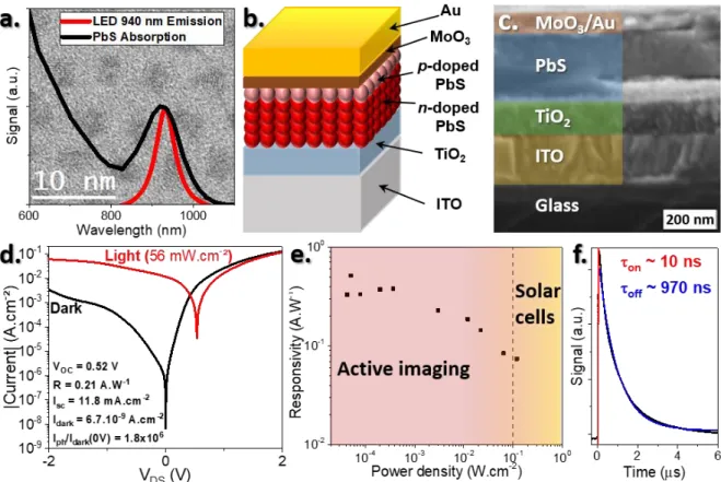
We start by synthetizing PbS nanocrystals with a peak band edge at 920 nm,31 see Figure 1a. This
wavelength is just below the targeted wavelength at 940 nm in order to take into account the redshift occurring during the ligand exchange procedure needed to build a conductive film. The diode structure follows the one proposed by Chuang et al.10 A thick tin-doped indium oxide (ITO) layer coupled with a
TiO2 layer is used as electron extractor. The absorbing layer is made of two layers of PbS. A thick (200
nm) n-type layer is built from a PbS ink32 with a high concentration (250 mg/mL) and I- as capping
ligands. A top p-type layer (≈20 nm) is deposited using a solid-state ligand exchange with ethanedithiol (EDT) as capping agent. The n- and p-type nature of each layer has been confirmed using ion-gel field effect transistor measurements, see figure S1. Finally, a thin MoO3 layer (10 nm) and gold contacts (80
nm) are used as hole extractor, see Figure 1b and c.
The I-V curve of the diode presents a strong rectifying behavior, see Figure 1d. The dark current at 0 V can be below 7 nA.cm-2, which is quite similar to the one reported for InGaAs sensor. Under
illumination by a 940 nm LED (at power density close to solar cell applications), the open circuit voltage reaches 0.52 V. This is slightly smaller than the 0.6 V value usually reported for solar cells, but the illumination here is quasi-monochromatic while solar light contains much higher energy photons. The short circuit current is 12 mA·cm-2, corresponding to a responsivity of 0.2 A.W-1 (EQE = 26%). The 0 V
signal-to-noise ratio is higher than 106. See the table S1 for a comparison of the performances of the
obtained diode with existing devices based on PbS nanocrystals.
The detectivity of the device has been estimated under low incident flux, see Figure S3a. Surprisingly, the noise is limited by white noise and no 1/f contribution33–35 has been identified in the measured
frequency range (1 Hz to 1 kHz), see figure S3b. Two factors tend to reduce the 1/f contributions which is generally the limiting contribution for the noise in nanocrystal array. First, the internanoparticle coupling is quite strong thanks to short ligand and this was identified as the main parameter driving the 1/f noise magnitude.34 Secondly, due to its relative wide band gap nature (compared to mid
infrared material), the device is quite resistive. The detectivity of the device at room temperature is 2 × 10¹² Jones, see Figure S3c.
Figure 1 : (a) Absorption spectrum (black) of PbS CQDs as synthetized (ligands: oleic acid (OA), solvent: toluene) and emission spectrum (red) of a 940 nm LED. Backfront: TEM image of PbS CQDs. (b) Scheme of the built diode. (c) Cross-section SEM image of the diode. (d) Dark current (black) and current under 940 nm excitation provided by a 940 nm LED (red) of the device. Some characteristics of the device are shown inset. (e) Diode responsivity at 0 V vs excitation provided by a 940 nm laser. (f) Time response of the device when excited by a 355 nm pulsed laser (1 ns pulse). Time constants τon and τoff are obtained
through a single exponential fit.
As the device aims at being operated under low incident photon flux, we have quantized the power dependence of the responsivity, see Figure 1e and S4. As often observed for nanocrystal-based photodetectors, the quantum efficiency is better under low photon flux and typically improves by a factor 10 as the photon flux is reduced by three orders of magnitude. A second figure of merit which is not accounted in the case of solar cells is the time response of the diode. Under 1 ns pulsed illumination, the rise time is 10 ns and the decay time is close to 1 µs, see figure 1f. This decay time is compatible with the RC time constant measured at high frequency (1-10 µs, see Figure S5). Impedance measurement reveals that the capacitance is almost independent of the frequency. As a result, under illumination the resistance of the sample drops and so does the RC time constant. This makes the turn on time significantly shorter than the decay time. Such time response is much faster than the one reported for PbS in photoconductive geometry.4 This is the combination of many factors (i) short
ligands lead to higher carrier mobility which combine with shorter electrode spacing and tend to reduce the transit time, (ii) switch to diode geometry suppress gain and make dynamics no longer limited by traps lifetime (at the cost of reduced gain), it also change the device capacitance and the RC relaxation time constant
Fast and intense response under low excitation flux are of utmost interest for the targeted pulsed active imaging application.
We then measure the photocurrent spectrum of the device and find it to be slightly blueshifted compared to the PbS film absorption spectrum, see Figure 2a. To understand this shift, we conduct electromagnetic simulations of the photodiode structure, using a frequency-domain modal method known as the Rigorous Coupled Wave analysis (RCWA),36 see part 4 of supplementary information for
details about the simulations. On part d, e and f of Figure 2 we respectively simulate the absorption map of the PbS layer, the ITO/TiO2/PbS stack and the full diode structure. Simulation reveals that (i)
loss in the contacts (both in ITO and gold) are a significant part of the total absorption (≈28 %), see Figure 2c, e and f. These losses are the result of the metal37 and ITO38 absorption in the visible and near
infrared. This problem remains mostly unaddressed for the design of solar cell while it may offer interesting perspective of improvement (ii) the diode structure introduces a Fabry-Perot resonance around 920 nm, see Figure 2c, and is responsible for the blue-shift of the photocurrent with respect to the absorption. Interestingly, this resonance spatially locates the maximum of absorption in the PbS film and not in the vicinity of the ITO contact, and rather close to the pn juction formed by the pbS(I)/PbS(EDT) interface. As a result the electromagnetic field is maximized where the electric field is also maximized. This explains the good efficiency of the current device in the near infrared. On the other hand, this will not be the case for shorter wavelength (with higher absorption coefficient) and this device appears not to be optimal for a solar cell perspective
Due to the Fabry-Perot resonance, the absorption magnitude is enhanced by a factor 5 when thin film (200 nm) of PbS are used. Increasing the film thickess (300 nm) is not really improving the device absorption since the increase of the PbS absorption layer is balanced by the reduction of the enhacement factor, see Figure S8.
Figure 2 : (a) Photocurrent of the full device (red) and absorption measured in transmission mode of the glass/ITO/TiO2/PbS stack (black) spectra of the device. (b) Simulated absorption spectra of a PbS
layer on glass (black), a PbS layer on ITO/TiO2/glass (blue) and the device (red). (c) Absorption ratio of
the device (red) and PbS on ITO/TiO2 (black) over PbS film absorption. Figures (d), (e), (f) correspond to
the modelized layers (left figure) and absorption distribution over the layers (right figure) under top illumination.
In NIR active imaging, the contrast observed on images results from differences in absorption and diffusion coefficients. This is typically useful for material sorting in order to discriminate the nature of illuminated objects. To mimic this application, we use a 940 nm laser source and shine its light onto plates made of different materials. We then measure the intensity of the scattered light at 0 V bias, see figure S6 for a scheme of the setup. The magnitude of the scattered light changes by almost three orders of magnitude depending on the material scattering the light, see figure 3a. This demonstrates the PbS photodiode ability to obtain pronounced contrast from a complex scene.
Outdoor active imaging requires collecting photons scattered over a long distance. As a proof of concept, we have tested the potential of our sensor to detect light scattered by a building located 85
m away from the source. A 10 W LED flashlight emitting at 940 nm is used as a source and is shone on the building in front of our laboratory (the estimated distance is 85 m, see Figure 3c). The collected signal is presented on Figure 3b. Even with a propagation distance around 170 m, a reasonable signal-to-noise ratio (≈ 3) is obtained.
Figure 3 : (a) Photocurrent of different materials from retrodiffused 940 nm laser light normalized by the photocurrent detected with a metallic plate. (b) Photocurrent modulation measured at 100 Hz as a function of time in a long range detection configuration. (c) Scheme of the long-range active imaging. A light source (10 W/940 nm lamp) enlights a building at a 85 m distance. The device detects retrodiffused light from the building.
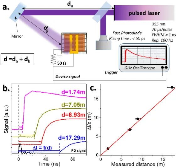
A second approach of active imaging is time-gated active imaging. The concept is to collect light after a delay to build an image corresponding to a given distance between the source and the scattering center. LIDAR detection is typically based on this concept. This obviously requires a fast detector where the rise time needs to be shorter than the light propagation time. In addition, the decay time of the photodetector needs to be also shorter than the inverse of the repetition rate of the illumination source. The fast time response of the diode at 0 V bias, shown in Figure 1d, is quite promising for such an application.
Figure 4 : (a) Scheme of the setup used for time-gating experiment. (b) Device response at 0 V as a function of the total distance from the source. The bottom black curve corresponds to the silicon photodiode (PD) response used for triggering. (c) Comparison between measured distances with a meter (X axis and red line) and deduced from ∆t determination. The red line is defined by y=x equation.
We use a 1 ns pulsed laser and tune the propagation distance from ≈ 2 m and up to ≈ 18 m, see Figure 4a. The PbS photodiode signal is collected on a GHz oscilloscope while a fast (50 ps) time response silicon diode is used as trigger. It is worth mentioning that we do not even use any amplification stage for this experiment. As the optical path is extended, we measure a clear increase of the delay between the reference signal from the fast photodiode and the one from the device, see Figure 4b. This delay is fully correlated with the light propagation distance, see Figure 4c. This validates the potential of the PbS photodiode for time gated imaging and its use to reconstruct a 3D scene.
We have revealed the potential of PbS solar cells used as near-infrared sensors for low cost active imaging at 940 nm. This conventional solar cell diode actually achieves large photoresponse (up to 0.5 A.W-1 under low photon flux) and fast time response (10 ns). Using electromagnetic simulations, we
have determined that the diode structure introduces a Fabry-Perot resonance which leads to a small blue-shift of the response. We also unveil that the absorption losses in the contacts represent 28% of the incident flux and this problem will have to be addressed in the future. We have demonstrated the
ability of the PbS photodiode to obtain contrast in complex scene, ability to make long distance detection at least up to 170 m and finally to be used for time-gated active imaging. Future work will have to expand these results to longer infrared wavelengths.39,40
METHODS
Chemicals: Octadecene (ODE, Acros Organics, 90%), Lead oxide (PbO, Strem Chemicals, 99.999+%-), Oleic acid (OA, Alfa Aesar 90%), Hexamethyldisilathiane (TMS2S, Sigma Aldrich, synthesis grade),
Ethanol (VWR, >99.9%), n-Octane (SDS, 99%), n-Heptane (Merck, >99%), n-Hexane (VWR, 99%), Toluene (Carlo Erba, >99.8%), N,N-Dimethylformamide (DMF, Sigma Aldrich), Hydrochloric acid (HCl, Mieuxa, 25%) Ammonium iodine (NH4I, Alfa Aesar, ≥ 99%), 1,2 Ethanedithiol (EDT, Fluka, 98%)
PbS nanocrystal synthesis: The procedure is inspired from Hines et al.31 0.9 g of PbO are introduced in
a 100 mL three neck flask with 3 g of OA and 47 g of ODE. The flask is degassed under vacuum at 120 °C for 2 hours. Meanwhile, in an air free glove box, a mixture of 420 µL of TMS2S and 10 mL of ODE is
prepared in a 20 mL vial, then introduced into a 20 mL syringe. The atmosphere of the flask is switched to Ar and the temperature is set equal to 90 °C. The TMS2S solution is quickly injected and the solution
turns dark while the temperature drops to 80 °C. After 8 min at 80 °C, the reaction is stopped by removing the heating mantle and prompt cooling of the flask by addition of a mixture of heptane and OA. The nanoparticles are then precipitated by addition of ethanol. The formed pellet is redispersed in toluene. A second step of cleaning is repeated. Finally, the pellet is redispersed in toluene with a 50 mg.mL-1 concentration. The solution is centrifuged to remove any colloidally unstable material. Finally,
the solution is filtered on a 0.22 µm PTFE filter.
PbS Ink preparation: A solution of NH4I at 60 mg.mL-1 in DMF is prepared by sonication. 2.5 mL of this
solution is introduced in a test tube. On the top of this polar phase, 2.5 mL of PbS nanocrystal solution at 50 mg.mL-1 is deposited. The two phases are then mixed and we observe a phase transfer. The clear
non-polar phase is discarded and the DMF solution is cleaned three more times using hexane. Finally, the particles are precipitated by introducing ethanol in the tube. After centrifugation the formed pellet is redispersed in fresh DMF with a concentration of 250 mg.mL-1. The solution is finally centrifuged to
discard any unstable material.
Solid state ligand exchange: A solution at 1% in mass of EDT in ethanol is prepared. A drop of PbS nanocrystals solution in hexane:octane (9:1 volume ratio) is drop-casted onto the electrodes and left to dry. The resulting thin film is dipped in the ligand solution and rinsed with acetone. Once the film is dried, a second layer of PbS nanocrystals is deposited and the ligand exchange step is repeated. The deposition process is performed two times in total.
ITO patterning: We start from commercial glass/ITO substrates of 30x30 mm² with a low sheet resistance (7 Ω/□). Substrates are cut into 15x15 mm² pieces and cleaned by sonication in an acetone bath during 5 min. The cleaning procedure is followed by rinsing the substrates with acetone and iso-propanol, then dried with a dry N2 flow. AZ 5214E photoresist is spin-coated for 30 s, then baked at
110 °C for 90 s. A standard photolithography process is performed using mask aligner for exposing the substrates to UV light for 5 s through a lithography mask (1 mm width). Photoresist is developed using AZ 726 developer for 20 s and immediately rinsed with deionized water. After that, exposed ITO surface is completely etched out with 25% HCl (in water) for 15 min at 40 °C, and substrates are immediately dipped into deionized water. Then, we conduct lift-off process in an acetone bath and patterned ITO substrates are cleaned with acetone and isopropanol. Finally, substrates are dried with dry N2 flow.
TiO2 film preparation: TiO2 films are prepared from a commercial solution (SOLARONIX Ti-Nanoxide
HT-L/SC). The solution is dropped on heated patterned ITO (110 °C) and spin-coated at 5000 rpm during 30 s. The pre-heating process is required in order to improve the solution wetting. Resulting ITO/TiO2
sample is then heated at 450 °C during 15 min and its thickness is measured to be 120 nm with DEKTAK profilometer.
n-doped PbS ink deposition: A 250 mg.mL-1 solution of n-doped PbS ink is used for the active material
layer. 60 µL of this solution is deposited on the ITO/TiO2 substrate and spin-coated at 1000 rpm during
60 s followed by 2000 rpm during 240 s. The procedure is repeated twice. Depositions are performed in air-free environment.
p-doped PbS: 60 µL of a 30 mg.mL-1 of OA capped PbS in toluene is deposited on the ITO/TiO
2/n-doped
PbS substrate and spin-coated at 2000 rpm during 30 s. A solid-state ligand exchange (see above) is then performed. This procedure is repeated twice. Depositions are performed in air-free environment. MoO3/Au deposition: After the deposition of PbS layers, the device is transferred from a glovebox to
an evaporator while keeping an air-free environment. After the glovebox-to-evaporator transfer and once a vacuum around 5.10-6 mbar is reached, 10 nm of MoO
3 followed by 80 nm of gold are
evaporated. The sample is then stored in air-free environment.
ASSOCIATED CONTENT SUPPORTING INFORMATIONS
Additional information about material characterization, diode and transistor fabrications and characterization, contrast-resolved measurement, noise and detectivity characterization, power dependent measurements, RC characterization as well as details about modelization are given in supporting information.
ACKNOWLEDEGMENTS
We thank Nexdot for providing the nanoparticles. EL thanks the support ERC starting grant blackQD (grant n°756225). We acknowledge the use of clean-room facilities from the “Centrale de Proximité Paris-Centre”. This work has been supported by the Region Ile-de-France in the framework of DIM Nano-K (grant dopQD). This work was supported by French state funds managed by the ANR within the”Investissements d'Avenir” program under reference ANR-11-IDEX-0004-02, and more specifically within the framework of the Cluster of Excellence MATISSE and also by the grant IPER-nano2, Frontal, Graskop and Copin.
REFERENCES
(1) Chen, H.; Liu, H.; Zhang, Z.; Hu, K.; Fang, X. Nanostructured Photodetectors: From Ultraviolet to Terahertz. Advanced Materials 2016, 28, 403–433.
(2) Goubet, N.; Jagtap, A.; Livache, C.; Martinez, B.; Portales, H.; Xu, X. Z.; Lobo, R. P. S. M.; Dubertret, B.; Lhuillier, E. Terahertz HgTe Nanocrystals: Beyond Confinement. J. Am. Chem. Soc. 2018, 140, 5033–5036.
(3) H. Sargent, E. Infrared Quantum Dots. Advanced Materials 2005, 17, 515–522.
(4) Konstantatos, G.; Howard, I.; Fischer, A.; Hoogland, S.; Clifford, J.; Klem, E.; Levina, L.; Sargent, E. H. Ultrasensitive Solution-Cast Quantum Dot Photodetectors. Nature 2006, 442, 180–183. (5) Konstantatos, G.; Sargent, E. H. PbS Colloidal Quantum Dot Photoconductive Photodetectors:
Transport, Traps, and Gain. Applied Physics Letters 2007, 91, 173505.
(6) Luther, J. M.; Gao, J.; Lloyd, M. T.; Semonin, O. E.; Beard, M. C.; Nozik, A. J. Stability Assessment on a 3% Bilayer PbS/ZnO Quantum Dot Heterojunction Solar Cell. Advanced Materials 2010, 22, 3704–3707.
(7) McDonald, S. A.; Konstantatos, G.; Zhang, S.; Cyr, P. W.; Klem, E. J. D.; Levina, L.; Sargent, E. H. Solution-Processed PbS Quantum Dot Infrared Photodetectors and Photovoltaics. Nature Materials 2005, 4, 138–142.
(8) Luther, J. M.; Law, M.; Beard, M. C.; Song, Q.; Reese, M. O.; Ellingson, R. J.; Nozik, A. J. Schottky Solar Cells Based on Colloidal Nanocrystal Films. Nano Lett. 2008, 8, 3488–3492.
(9) Semonin, O. E.; Luther, J. M.; Choi, S.; Chen, H.-Y.; Gao, J.; Nozik, A. J.; Beard, M. C. Peak External Photocurrent Quantum Efficiency Exceeding 100% via MEG in a Quantum Dot Solar Cell. Science 2011, 334, 1530–1533.
(10) Chuang, C.-H. M.; Brown, P. R.; Bulovic, V.; Bawendi, M. G. Improved Performance and Stability in Quantum Dot Solar Cells through Band Alignment Engineering. Nat. Mater. 2014, 13, 796– 801.
(11) Tang, J.; Kemp, K. W.; Hoogland, S.; Jeong, K. S.; Liu, H.; Levina, L.; Furukawa, M.; Wang, X.; Debnath, R.; Cha, D.; et al. Colloidal-Quantum-Dot Photovoltaics Using Atomic-Ligand Passivation. Nat. Mater. 2011, 10, 765–771.
(12) Protesescu, L.; Yakunin, S.; Bodnarchuk, M. I.; Krieg, F.; Caputo, R.; Hendon, C. H.; Yang, R. X.; Walsh, A.; Kovalenko, M. V. Nanocrystals of Cesium Lead Halide Perovskites (CsPbX3 , X = Cl, Br,
and I): Novel Optoelectronic Materials Showing Bright Emission with Wide Color Gamut. Nano Letters 2015, 15, 3692–3696.
(13) Sanehira, E. M.; Marshall, A. R.; Christians, J. A.; Harvey, S. P.; Ciesielski, P. N.; Wheeler, L. M.; Schulz, P.; Lin, L. Y.; Beard, M. C.; Luther, J. M. Enhanced Mobility CsPbI3 Quantum Dot Arrays for Record-Efficiency, High-Voltage Photovoltaic Cells. Sci. Adv. 2017, 3, eaao4204.
(14) Swarnkar, A.; Marshall, A. R.; Sanehira, E. M.; Chernomordik, B. D.; Moore, D. T.; Christians, J. A.; Chakrabarti, T.; Luther, J. M. Quantum Dot-Induced Phase Stabilization of Alpha-CsPbI3
Perovskite for High-Efficiency Photovoltaics. Science 2016, 354, 92–95.
(15) Bederak, D.; Balazs, D. M.; Sukharevska, N. V.; Shulga, A. G.; Abdu-Aguye, M.; Dirin, D. N.; Kovalenko, M. V.; Loi, M. A. Comparing Halide Ligands in PbS Colloidal Quantum Dots for Field-Effect Transistors and Solar Cells. ACS Applied Nano Materials 2018, 1, 6882–6889.
(16) Lu, K.; Wang, Y.; Liu, Z.; Han, L.; Shi, G.; Fang, H.; Chen, J.; Ye, X.; Chen, S.; Yang, F.; et al. High-Efficiency PbS Quantum-Dot Solar Cells with Greatly Simplified Fabrication Processing via “Solvent-Curing.” Adv. Mater. 2018, 30, 1707572.
(17) Hafiz, S. B.; Scimeca, M.; Sahu, A.; Ko, D.-K. Colloidal Quantum Dots for Thermal Infrared Sensing and Imaging. Nano Convergence 2019, 6, 7.
(18) Lhuillier, E.; Guyot-Sionnest, P. Recent Progresses in Mid Infrared Nanocrystal Optoelectronics. IEEE Journal of Selected Topics in Quantum Electronics 2017, 23, 1–8.
(19) Livache, C.; Martinez, B.; Goubet, N.; Ramade, J.; Lhuillier, E. Road Map for Nanocrystal Based Infrared Photodetectors. Front. Chem. 2018, 6, 575.
(20) Lu, H.; Carroll, G. M.; Neale, N. R.; Beard, M. C. Infrared Quantum Dots: Progress, Challenges, and Opportunities. ACS Nano 2019, 13, 939–953.
(21) Jean, J.; Mahony, T. S.; Bozyigit, D.; Sponseller, M.; Holovsky, J.; Bawendi, M. G.; Bulovic, V. Radiative Efficiency Limit with Band Tailing Exceeds 30% for Quantum Dot Solar Cells. ACS Energy Lett. 2017, 2, 2616–2624.
(22) Chuang, C.-H. M.; Maurano, A.; Brandt, R. E.; Hwang, G. W.; Jean, J.; Buonassisi, T.; Bulovic, V.; Bawendi, M. G. Open-Circuit Voltage Deficit, Radiative Sub-Bandgap States, and Prospects in Quantum Dot Solar Cells. Nano Lett. 2015, 15, 3286–3294.
(23) Bi, Y.; Pradhan, S.; Gupta, S.; Akgul, M. Z.; Stavrinadis, A.; Konstantatos, G. Infrared Solution-Processed Quantum Dot Solar Cells Reaching External Quantum Efficiency of 80% at 1.35 Mu m and JSc in Excess of 34 mA cm-2. Adv. Mater. 2018, 30, 1704928.
(24) Rauch, T.; Böberl, M.; Tedde, S. F.; Fürst, J.; Kovalenko, M. V.; Hesser, G.; Lemmer, U.; Heiss, W.; Hayden, O. Near-Infrared Imaging with Quantum-Dot-Sensitized Organic Photodiodes. Nature Photonics 2009, 3, 332–336.
(25) Georgitzikis, E.; Malinowski, P. E.; Li, Y.; Maes, J.; Hagelsieb, L. M.; Guerrieri, S.; Hens, Z.; Heremans, P.; Cheyns, D. Integration of PbS Quantum Dot Photodiodes on Silicon for NIR Imaging. IEEE Sensors Journal 2019, 1–1.
(26) Georgitzikis, E.; Malinowski, P. E.; Maes, J.; Hadipour, A.; Hens, Z.; Heremans, P.; Cheyns, D. Optimization of Charge Carrier Extraction in Colloidal Quantum Dots Short-Wave Infrared Photodiodes through Optical Engineering. Advanced Functional Materials 2018, 28, 1804502. (27) Tang, X.; Ackerman, M. M.; Shen, G.; Guyot-Sionnest, P. Towards Infrared Electronic Eyes:
Flexible Colloidal Quantum Dot Photovoltaic Detectors Enhanced by Resonant Cavity. Small 2019, 15, 1804920.
(28) Tang, X.; Ackerman, M. M.; Chen, M.; Guyot-Sionnest, P. Dual-Band Infrared Imaging Using Stacked Colloidal Quantum Dot Photodiodes. Nature Photonics 2019, 13, 277–282.
(29) Temple, D. S.; Hilton, A.; Klem, E. J. D. Towards Low-Cost Infrared Imagers: How to Leverage Si IC Ecosystem; Proc SPIE 2016; 9989 99890E.
(30) Klem, E. J. D.; Gregory, C.; Temple, D.; Lewis, J. PbS Colloidal Quantum Dot Photodiodes for Low-Cost SWIR Sensing. Proc SPIE 2015; 9451, 945104.
(31) Hines, M. A.; Scholes, G. D. Colloidal PbS Nanocrystals with Size-Tunable near-Infrared Emission: Observation of Post-Synthesis Self-Narrowing of the Particle Size Distribution. Adv. Mater. 2003, 15, 1844–1849.
(32) Kim, J.; Ouellette, O.; Voznyy, O.; Wei, M.; Choi, J.; Choi, M.-J.; Jo, J. W.; Baek, S.-W.; Fan, J.; Saidaminov, M. I.; et al. Butylamine-Catalyzed Synthesis of Nanocrystal Inks Enables Efficient Infrared CQD Solar Cells. Adv. Mater. 2018, 30, 1803830.
(33) De Iacovo, A.; Venettacci, C.; Colace, L.; Scopa, L.; Foglia, S. Noise Performance of PbS Colloidal Quantum Dot Photodetectors. Appl. Phys. Lett. 2017, 111, 211104.
(34) Liu, H.; Lhuillier, E.; Guyot-Sionnest, P. 1/f Noise in Semiconductor and Metal Nanocrystal Solids. J. Appl. Phys. 2014, 115, 154309.
(35) Lai, Y.; Li, H.; Kim, D. K.; Diroll, B. T.; Murray, C. B.; Kagan, C. R. Low-Frequency (1/f) Noise in Nanocrystal Field-Effect Transistors. ACS Nano 2014, 8, 9664–9672.
(36) Hugonin, J.-P.; Lalanne, P. Reticolo Software for Grating Analysis. 2005.
(37) Olmon, R. L.; Slovick, B.; Johnson, T. W.; Shelton, D.; Oh, S.-H.; Boreman, G. D.; Raschke, M. B. Optical Dielectric Function of Gold. Phys. Rev. B 2012, 86, 235147.
(38) Holman, Z. C.; Filipic, M.; Descoeudres, A.; De Wolf, S.; Smole, F.; Topic, M.; Ballif, C. Infrared Light Management in High-Efficiency Silicon Heterojunction and Rear-Passivated Solar Cells. J. Appl. Phys. 2013, 113, 013107.
(39) Cryer, M. E.; Halpert, J. E. 300 nm Spectral Resolution in the Mid-Infrared with Robust, High Responsivity Flexible Colloidal Quantum Dot Devices at Room Temperature. ACS Photonics 2018, 5, 3009–3015.
(40) Killilea, N.; Wu, M.; Sytnyk, M.; Amin, A. A. Y.; Mashkov, O.; Spiecker, E.; Heiss, W. Pushing PbS/Metal-Halide-Perovskite Core/Epitaxial-Ligand-Shell Nanocrystal Photodetectors beyond 3 µm Wavelength. Advanced Functional Materials 2019, 29, 1807964.