HAL Id: hal-02122049
https://hal.archives-ouvertes.fr/hal-02122049
Submitted on 30 Oct 2019HAL is a multi-disciplinary open access archive for the deposit and dissemination of sci-entific research documents, whether they are pub-lished or not. The documents may come from teaching and research institutions in France or abroad, or from public or private research centers.
L’archive ouverte pluridisciplinaire HAL, est destinée au dépôt et à la diffusion de documents scientifiques de niveau recherche, publiés ou non, émanant des établissements d’enseignement et de recherche français ou étrangers, des laboratoires publics ou privés.
Field effect transistor and photo transistor of narrow
band gap nanocrystal arrays using ionic glasses
Charlie Gréboval, Ulrich Noumbe, Nicolas Goubet, Clément Livache, Julien
Ramade, Junling Qu, Audrey Chu, Bertille Martinez, Yoann Prado, Sandrine
Ithurria, et al.
To cite this version:
Charlie Gréboval, Ulrich Noumbe, Nicolas Goubet, Clément Livache, Julien Ramade, et al.. Field effect transistor and photo transistor of narrow band gap nanocrystal arrays using ionic glasses. Nano Letters, American Chemical Society, 2019, 19 (6), pp.3981-3986. �10.1021/acs.nanolett.9b01305�. �hal-02122049�
Field effect transistor and photo transistor of narrow band gap nanocrystal arrays using
ionic glasses
Charlie Gréboval
1, Ulrich Noumbe
2, Nicolas Goubet
1,3,
Clément Livache
1,3, Julien Ramade
1, Junling Qu
1,
Audrey Chu
1, Bertille Martinez
1,3, Yoann Prado
1, Sandrine Ithurria
3, Abdelkarim Ouerghi
4, Herve Aubin
4,
Jean-Francois Dayen
2*, Emmanuel Lhuillier
1*1 Sorbonne Université, CNRS, Institut des NanoSciences de Paris, INSP, F-75005 Paris, France.
2 Université de Strasbourg, CNRS, Institut de Physique et Chimie des Matériaux de Strasbourg (IPCMS), UMR 7504,
F-67000 Strasbourg, France.
3 Laboratoire de Physique et d’Étude des Matériaux, ESPCI-Paris, PSL Research University, Sorbonne Université Univ
Paris 06, CNRS UMR 8213, 10 rue Vauquelin, 75005 Paris, France.
4 Centre de Nanosciences et de Nanotechnologies, CNRS, Université Paris-Sud, Université Paris-Saclay, C2N–
Marcoussis, 91460 Marcoussis, France
Abstract: Gating of nanocrystal films is currently driven by two approaches: either the use of a dielectric such as SiO2
or the use of electrolyte. SiO2 allows fast bias sweeping over a broad range of temperatures but requires a large
operating bias. Electrolyte, thanks to a large capacitance, leads to significantly reduce operating bias but is limited to slow speed and quasi room temperature operation. None of these operating conditions are optimal for narrow band gap nanocrystal-based phototransistors for which the need of a large capacitance gate has to be combined with low temperature operation. Here we explore the use of a LaF3 ionic glass as a high capacitance gating alternative. We
demonstrate for the first time the use of such ionic glasses to gate thin films made of HgTe and PbS nanocrystals. This gating strategy allows operation in the 180 to 300 K range of temperatures with capacitance as high as 1 µF·cm-2. We
unveil the unique property of ionic glass gate to enable unprecedented tunability of both magnitude and dynamics of the photocurrent, thanks to high charge doping capability within an operating temperature window relevant for infrared photodetection. We demonstrate that by carefully choosing the operating gate bias, the signal to noise ratio can be improved by a factor 100 and the time response accelerated by a factor 6. Moreover, the good transparency of LaF3 substrate allows back side illumination in the infrared which is highly valuable for the design of
phototransistors.
To whom correspondence should be sent: el@insp.upmc.fr, dayen@unistra.fr
INTRODUCTION
Narrow band gap nanocrystals1–3 are currently generating a strong interest for the design of high performance and
low cost infrared sensors in the short-wave (SWIR: up to 1.7 µm) and mid-wave infrared (MWIR : 3-5 µm).4,5 Recent
developments include high detectivity photodiodes,6 multicolor devices,7–9 demonstration of focal plane arrays10 and
detectors with enhanced light matter coupling.11–14 A possible strategy to go beyond the photoconductive geometry
relates to phototransistors.15–17 In this case, the field effect transistor (FET) is not used to probe the majority carriers
of the film but rather to bring the thin film in an operating point which maximizes the signal to noise ratio,5 mostly by
reducing the dark current.
Two main strategies have been developed to gate nanocrystal films. (i) Historically, gate effect of nanocrystal arrays18
was obtained through a dielectric layer of SiO2.19 The method has the advantage of being simple to implement but
requires high operating biases and is limited by possible electrical breakdown. The use of high-k materials20 such as
HfO2, Al2O3,21,22 or TiO2 have been proposed as a possible improvement strategy. (ii) Alternatively, gating of nanocrystal
films can be obtained using electrolyte.23–26 Because ions from the electrolyte can percolate within the bulk of the
nanocrystal film, thick film gating is possible and is of utmost interest to combine a large absorption with a gate effect. With electrolytes, the sheet gate capacitance is no longer driven by the ratio of the dielectric constant to the dielectric thickness, but rather by the ratio of the dielectric constant to the thickness of the ionic double layer. The latter thickness is typically around 1 nm, which allows for fairly large capacitances. A key consequence is to allow low bias operation27 for the device but even more important is the possibility to achieve massive charge injection within the
nanocrystals up to several carriers per dot. As a result, it becomes possible to tune the nanocrystal spectrum by injecting electrons in the film up to the point that interband transition is bleached and intraband transition in the mid-infrared appears.28 On the other hand, electrolyte requires relatively high operating temperatures. Such constrain is
poorly compatible with infrared materials that generally requires low temperature operation. With electrolyte, it is possible to prepare the system in a given charging state at high temperature, but the carrier density tunability is lost at low temperature. This makes that the two main conventional methods to gate nanocrystal films are not fully satisfying for the design of infrared phototransistors based on colloidal nanocrystals. Moreover, it may be delicate in some cases to control and asset the doping processes (electrostatic or electrochemical29) while they may deeply
influence the device properties.30–33 Ferro-electric gating, which takes advantage of the divergence of the material
dielectric constant in the vicinity of the Curie temperature has also been explored. Derivative of poly(vinylidene fluoride) (PVDF) presents dielectric constant above 35 at room temperature.34 However, this approach is limited to
room temperature and requires the use of other ferroelectric materials if temperatures in the 150-300 K range are targeted. This range of temperatures typically corresponds to operating temperatures of detectors in the SWIR and MWIR range of wavelengths.
In this letter, we explore the possibility to use ionic glasses as a path to induce gate effect in nanocrystal arrays. This approach has first been developed by the Shukla’s group35,36 on 2D materials using conventional glass. The glass is first
melted at high temperature to give ions some mobility and a large electric field is applied over the substrate to make them move. Conventional glass, however, requires operating temperature around 500 °C which is incompatible with nanocrystals, for which melting temperatures are far below. This is especially the case for lead and mercury chalcogenides commonly used in the infrared, whose synthesis temperatures are around 80 to 150°C. Recently, the Cui’s group explored the use of LaF3 as an ionic glass to induce a gate effect in a MoS2 flake.37 LaF3 is originally used for
infrared optics and presents a strong transparency in the mid infrared, which is promising to design phototransistors with back side illumination. In addition, ionic mobilities remain high enough to induce gating for temperatures down to 180 K. Here, we explore the use of such LaF3 glasses as substrate to induce gate effect in thin films of HgTe
nanocrystals. We compare the obtained performances with conventional dielectric gating through SiO2 and with
electrolyte. We also determine the range of operating temperatures and frequencies compatible with this new gate technology. Finally, we demonstrate that not only the dark conductance can be controlled with the ionic glass gate but also the photoresponse.
DISCUSSION
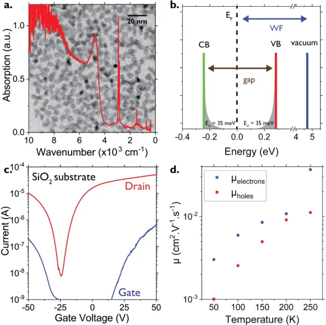
We first start by synthetizing HgTe nanocrystals with a band edge energy around 500 meV (≈ 4000 cm-1 or 2.5 µm)
using an established procedure,38 see Figure 1a. The obtained nanocrystals have a tetrapodic shape, see Figure 1a. The
electronic structure (energy location of conduction and valence band, relative position of Fermi level and in-gap trap states) of this material has been previously determined using a combination of infrared spectroscopy, photoemission spectroscopy39 and time-resolved photocurrent measurements.40 Typically, the material presents a 4.6 eV work
function. The Fermi level is within the band gap but clearly lies closer to the conduction band and the Urbach energy describing the amount of trap states within the band gap has been estimated to be 35 meV for ethanedithiol capped nanoparticles, see Figure 1b.
Figure 1 (a) Absorption spectrum of HgTe nanocrystals with a band edge at 4000 cm-1 (2.5 µm). Background:
transmission electron microscopy image of the material showing tetrapods nanoparticles. (b) Electronic structure of the HgTe nanocrystals, adapted with permission from ref 39 (c) Transfer curve of a film of HgTe nanocrystals on a Si/SiO2 substrate in a back-gate configuration and under 1 V drain-source bias. Channel current in red and gate leakage
current in blue. (d) Holes and electrons mobilities measured in back-gate configuration for different temperatures.
The transport properties of the HgTe nanocrystal array have first been tested using a conventional SiO2 gate. In this
case, a dry layer of oxide with a 300 nm thickness is used as dielectric. To ensure a strong interparticle coupling, we use a liquid phase transfer approach, where the HgTe nanocrystals end up being capped in solution with short thiol, see methods for details. The thin film presents an ambipolar character with both hole and electron conduction, consistent with previous measurements obtained with electrolyte gating,28,41,42 see Figure 1c. The linear mobilities of
electrons and holes have been estimated using the expression µ = 𝐿
𝑊𝐶𝛴𝑉𝐷𝑆
𝜕𝐼𝐷𝑆
𝜕𝑉𝐺𝑆, where L is the electrode spacing (10 µm), W is the electrode length (49 × 2.5 mm), CΣ the surface capacitance equal to 11.5 nF.cm-2 for 300 nm thick SiO2
layer and VDS the drain source bias. We found that electron mobility is typically a factor 3 larger than the hole mobility
and reaches 3 x 10⁻² cm2·V-1·s-1 at room temperature,43 see Figure 1d.
Figure 2 (a) Scheme of a HgTe back-gate FET on SiO2 when Vgs > 0. (b) Scheme of a HgTe back-gate FET on LaF3 when
Vgs > 0. (c) Scheme of a HgTe top-gate FET with LiClO4 electrolyte when Vgs > 0. (d) Typical transfer curves obtained for
HgTe nanocrystals with different gating techniques. SiO2 and LaF3 are measured at 200 K, electrolyte one is measured
at 300 K. (e) On/Off ratios of FET curves measured at different temperatures for different gating configurations. Ratios are normalized by the ratio at the highest temperature for each gating configuration. (f) On/Off ratios normalized by the ratio at the lowest sweep rate for each gating configuration measured at different sweep rates of VGS for each
gating configuration.
Now that the FET properties of the HgTe nanocrystal array are established using a conventional gate, we compare the properties of the film while gate effect results from (i) SiO2 dielectric layer, see Figure 2a, (ii) LaF3 ionic glass, see Figure
2b and (iii) electrolyte, Figure 2c. For dielectric material, the gate effect results from the generation of charges at the dielectric surface, see Figure 2a and S1. For ionic glass, there is in addition to the dielectric capacitance through the thick (1.1 mm) substrate a gating induced by the mobility of the F- vacancies, see Figure 2b and S2. For electrolyte,
gating is the result of the ions from the electrolyte that move inside the nanocrystal film and surround nanocrystals, see Figure 2c and S3. For both technologies, we observe a drain current modulation reaching three orders of magnitude, see Figure 2d. However, a gate bias range of 100 V is required for SiO2, while only 10 V are necessary in
the case of LaF3 (20 V at low temperature) and 4 V in the case of electrolyte. While the electrolyte appears as the most
efficient gate at room temperature, its efficiency quickly drops as temperature is reduced, see Figure 2e. Already at 260 K, no current modulation can be obtained. On the other hand, both SiO2 and LaF3, preserve their gate effect down
host matrix is used. This result is a severe limitation of the sweep rate modulation, see Figure 2f. In the case of electrolyte, faster current modulation is possible by replacing the polymer matrix by a liquid solvent, but it makes the device far more sensitive to moisture and the ability to operate the device in air is lost. The SiO2 gate is fully compatible
with fast sweep rate while LaF3 presents an intermediate trade off. Table 1 summarizes the different advantages and
limitations of each technology.
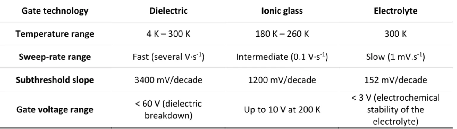
Table 1 Typical ranges of use for solid state gating of HgTe nanocrystal based field effect transistor.
Gate technology Dielectric Ionic glass Electrolyte
Temperature range 4 K – 300 K 180 K – 260 K 300 K
Sweep-rate range Fast (several V·s-1) Intermediate (0.1 V·s-1) Slow (1 mV.s-1)
Subthreshold slope 3400 mV/decade 1200 mV/decade 152 mV/decade
Gate voltage range < 60 V (dielectric
breakdown) Up to 10 V at 200 K
< 3 V (electrochemical stability of the
electrolyte)
It is worth noting that the ionic glass gating is not limited to HgTe nanocrystals. In figure S4, we have demonstrated the gating of thin films of PbS. The gating mechanism of each technology can be further revealed using impedance spectroscopy, see Figure 3 and S5. The SiO2 as dielectric presents a frequency independent capacitance, see Figure 3a.
Similar behavior is observed on the electrolyte and the ionic glass at high frequency, typically above 1-10 kHz. In this range of frequencies, the capacitance obtained for the electrolyte and ionic glass are weaker than for SiO2, mostly due
to the large thickness of LaF3 substrate or electrolyte (≈1 mm typically, compared to 300 nm for SiO2). At low frequency,
the capacitance of ionic glass and electrolyte strongly increases. This rise is associated with the displacement of ions (Li+/ClO
4- in the case of electrolyte, F- vacancies in the case of LaF3) which form an ionic double layer.32 This
understanding is supported by the temperature dependence of the capacitance versus frequency, see Figure 3b. The capacitance at high frequency is temperature independent. This reflects the poor temperature dependency of the dielectric constant. On the other hand, the low frequency increase of the capacitance presents a large temperature dependence which reflects the activation of the ionic mobility with temperature. However, at the lowest frequency range, the capacitance tends towards an extremum value in the case of ionic glass gate, while for electrolyte gating, it is getting higher as the frequency decreases. This phenomenon in electrolyte systems is a signature of the triggering of electrochemical doping process. We can then confirm that ionic glass technology prevents electrochemical doping process at the relevant frequency range for device application.
Figure 3 (a) Capacitance of gate measured at 300 K under 300 mV AC signal for different gating configurations. (b) Evolution of the capacitance with frequency for different temperatures on LaF3 substrate under 300 mV AC signal. The
inset is an equivalent circuit of the LaF3 gate
At 300 K and low frequency, sheet capacitance as large as 1 µF·cm-2 can be achieved. Applying 5 V of gate bias leads
to a sheet density as large as 3 x 10¹³ carrier·cm-2. The value of capacitance can also be used to determine the mobility
of the film obtained with the LaF3 gate. As the frequency dependence of the capacitance becomes weak at low
frequency, we can assume a gate capacitance of 500 nF·cm-2 with LaF
3, which leads to mobility of 1.5 x 10⁻² cm2·V-1·s-1
for the holes and 4 x 10⁻² cm2·V-1·s-1 for the electrons. This is exactly the same values that we have obtained with the
SiO2 gating.
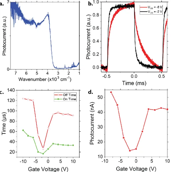
To finish we have tested the potential of this gate to also control the photocurrent generation. Using a Fourier Transform Infrared (FTIR) spectrometer, see Figure S6 for a scheme of the setup, we have measured the photocurrent spectrum, see Figure 4a. The good correlation between the absorption spectrum and the photocurrent spectrum confirms that the photocurrent is coming from the nanocrystal film. The time response of the system can be tested by exciting the system with a pulsed laser diode operating at 1.55 µm. This wavelength has been chosen to be close enough to the band edge (1.6 x the band edge energy) to avoid any hot electron effect such as multi exciton generation.44
Figure 4 (a) Photocurrent spectrum of HgTe nanocrystal film on a LaF3 substrate at 200 K under 0 V VGS. (b)
Photoresponse at 1 kHz of a HgTe film on LaF3 device under 4 mW at 1.55 µm excitation for two gate voltages. (c)
Response times at 1 kHz measured at 200 K for different gate voltages under 4 mW at 1.55 µm excitation. (d) Photocurrent at 1 kHz measured under 4 mW at 1.55 µm excitation for different gate voltages at 200 K.
The gate bias strongly impacts the photoresponse dynamics, see Figure 4b and c. The time response (on and off time) are faster when the gate bias corresponds to the minimum of conductance of the dark current transfer curve. A modulation of a factor 6 of the carrier dynamics can be induced by the gate. The dynamics under hole injection is slightly slower than the one reported for electron. However, the balance of the carrier dynamics between the electron rich and hole rich material is much better than the one previously reported using long thiol chain (heptanedithiol) as capping ligand, for which hole dynamics was 100 times faster than the one measured for electrons.42 It is also
interesting to note that the fastening of the response comes with a decrease of the magnitude of the photoresponse, see Figure 4d. In this sense the modulation of the photocurrent is made at quasi constant gain-bandwidth product.8
However the drop of the photoresponse (roughly a factor 10) when the system is at its minimum of conductance is much smaller than the one measured for the dark conductance (almost a factor 1000). In this sense, using the gate to prepare the system at its minimum of conductance leads to an increase of the signal to noise ratio (ie detectivity) by almost two orders of magnitude, while fastening the response by a factor 6. To finish the discussion relative to the gate-controlled dynamics, one may wonder what the physical phenomenon behind the observed dynamics is. The latter may result from transport phenomenon, in this case the RC time constant will drive the dynamics of the photocurrent. This is unlikely to be the case here. Indeed, the ambipolar character of the sample makes that resistance is maximum close to zero gate bias, thus the longest RC time constant are expected close to zero volt, while this bias corresponds to the one where the fastest time response have been obtained, see Figure 4c. Alternatively, the observed dynamics may be driven by traps and recombination. In particular, mid band gap recombination centers are expected to be ineffective when the Fermi level is located within a band, since they cannot change their charge states. In this case, long dynamics (ie low recombination rate) are predicted. On the other hand, as the Fermi level is close to the middle of the gap, as it is the case when the gate bias is close to zero, the recombination centers can change their charge states and efficiently behave as recombination centers that increase the recombination rate. This picture matches well with the observed dynamics which are faster if gate bias brings the Fermi level around the middle of the band gap.
CONCLUSION
We have demonstrated the potential of LaF3 ionic glass as a high capacitance gate for the design of low temperature
operated field effect transistors and phototransistors. The capacitance of the ionic glass is the combination of a low value dielectric capacitance and an ionic double layer higher capacitance resulting from F- vacancy at low frequency.
This strategy allows to achieve sheet capacitance as high as 1 µF·cm-2, and sheet carrier concentration exceeding 3-5
1013 carrier·cm-2, very close to the reported value for electrolyte gating, while preserving the gate tunability down to
180 K. The generality of the method is demonstrated by building FET from PbS thin films. Finally, we unveil how this strategy can be used to control the magnitude of the nanocrystal photoresponse. We demonstrate that by carefully choosing the operating bias, the signal to noise can be enhanced by a factor 100 and the response time fasten by a factor 6.
ACKNOWLEDEGMENTS
EL thanks the support ERC starting grant blackQD (grant n° 756225). We acknowledge the use of clean-room facilities from the “Centrale de Proximité Paris-Centre”. This work has been supported by the Region Ile-de-France in the framework of DIM Nano-K (grant dopQD). This work was supported by French state funds managed by the ANR within the Investissements d'Avenir programme under reference ANR-11-IDEX-0004-02, and more specifically within the framework of the Cluster of Excellence MATISSE and also by the grant IPER-Nano2 and H2DH. JQ thanks Chinese Scholar council for PhD grant while NG and JR thank Nexdot for post doc funding. JFD thanks financial support of the Agence Nationale de la Recherche (Labex NIE 11-LABX-0058_NIE within the Investissement d’Avenir program ANR-10-IDEX-0002-02). The authors thank the members of the StNano platform for their technical assistance during nanofabrication.
SUPPORTING INFORMATION
Supporting Information include details about material synthesis and characterization, additional transistor fabrication details and measurements.
COMPETING INTEREST
The authors declare no competing financial interest.
REFERENCES
(1) Kershaw, S. V.; Susha, A. S.; Rogach, A. L. Chem. Soc. Rev. 2013, 42, 3033–3087.
(2) Killilea, N.; Wu, M.; Sytnyk, M.; Yousefi Amin, A. A.; Mashkov, O.; Spiecker, E.; Heiss, W. Adv. Funct. Mater. 2019, 29, 1807964.
(3) Keuleyan, S.; Lhuillier, E.; Brajuskovic, V.; Guyot-Sionnest, P. Nat. Photonics 2011, 5, 489–493. (4) Lhuillier, E.; Guyot-Sionnest, P. IEEE J. Sel. Top. Quantum Electron. 2017, 23, 1–8.
(5) Livache, C.; Martinez, B.; Goubet, N.; Ramade, J.; Lhuillier, E. Front. Chem. 2018, 6, 575. (6) Ackerman, M. M.; Tang, X.; Guyot-Sionnest, P. ACS Nano 2018, 12, 7264–7271.
(7) Tang, X.; Ackerman, M. M.; Chen, M.; Guyot-Sionnest, P. Nat. Photonics 2019 2019, 13, 277–282.
(8) Lhuillier, E.; Robin, A.; Ithurria, S.; Aubin, H.; Dubertret, B.; Lhuillier, E.; Ithurria, S.; Robin, A. Nano Lett. 2014,
14, 2715–2719.
(9) Tang, X.; Tang, X.; Lai, K. W. C. ACS Photonics 2016, 3, 2396–2404.
(10) Martinez, B.; Livache, C.; Goubet, N.; Chu, A.; Gréboval, C.; Ramade, J.; Qu, J.; Becerra, L.; Dandeu, E.; Fave, J. L.; et al. Adv. Opt. Mater. 2019.
(11) Chen, M.; Shao, L.; Kershaw, S. V.; Yu, H.; Wang, J.; Rogach, A. L.; Zhao, N. ACS Nano 2014, 8, 8208–8216. (12) Tang, X.; Wu, G. fu; Lai, K. W. C. J. Mater. Chem. C 2017, 5, 362–369.
(13) Tang, X.; Ackerman, M. M.; Guyot-Sionnest, P. ACS Nano 2018, 12, 7362–7370.
(14) Tang, X.; Ackerman, M. M.; Shen, G.; Guyot-Sionnest, P. Small 2019, 1804920, 1804920.
(15) Detavernier, C.; Gassenq, A.; Hu, C.; Chen, H.; Hens, Z.; Justo, Y.; Roelkens, G.; Devloo-Casier, K. Appl. Phys. Lett. 2014, 105, 171110.
(16) Chen, M.; Lu, H.; Abdelazim, N. M.; Zhu, Y.; Wang, Z.; Ren, W.; Kershaw, S. V.; Rogach, A. L.; Zhao, N. ACS Nano 2017, 11, 5614–5622.
(17) List, E. J. W.; Gamerith, S.; Heiss, W.; Böberl, M.; Kovalenko, M. V. Adv. Mater. 2007, 19, 3574–3578. (18) Hetsch, F.; Zhao, N.; Kershaw, S. V.; Rogach, A. L. Mater. Today 2013, 16, 312–325.
(19) Talapin, D. V.; Murray, C. B. Science 2005, 310, 86–89.
(20) Chung, D. S.; Lee, J. S.; Huang, J.; Nag, A.; Ithurria, S.; Talapin, D. V. Nano Lett. 2012, 12, 1813–1820. (21) Kim, H.; Cho, K.; Kim, D. W.; Lee, H. R.; Kim, S. Appl. Phys. Lett. 2006, 89, 173107.
2013, 13, 1578–1587.
(23) Kang, M. S.; Sahu, A.; Norris, D. J.; Frisbie, C. D. Nano Lett. 2011, 11, 3887–3892. (24) Yu, D.; Wang, C.; Guyot-Sionnest, P. Science 2003, 300, 1277–1280.
(25) Kang, M. S.; Sahu, A.; Norris, D. J.; Frisbie, C. D. Nano Lett. 2010, 10, 3727–3732.
(26) Roest, A. L.; Meulenkamp, E. A.; Delerue, C.; Germeau, A.; Allan, G.; Vanmaekelbergh, D. Phys. Rev. Lett. 2003,
90, 097401.
(27) Loi, M. A.; Heiss, W.; Bisri, S. Z.; Piliego, C.; Yarema, M. Adv. Mater. 2013, 25, 4309–4314. (28) Wang, C.; Shim, M.; Guyot-Sionnest, P. Science 2001, 291, 2390–2392.
(29) Kim, S. H.; Hong, K.; Xie, W.; Lee, K. H.; Zhang, S.; Lodge, T. P.; Frisbie, C. D. Adv. Mater. 2013, 25, 1822–1846. (30) Frisbie, C. D.; Leighton, C.; Walter, J.; Luo, B.; Wang, H. ACS Nano 2016, 10, 7799–7810.
(31) Saito, R.; Kong, J.; Dresselhaus, M. S.; Farhat, H.; Sasaki, K.-I.; Kavan, L.; Kalbac, M. ACS Nano 2009, 3, 2320– 2328.
(32) Yuan, H.; Shimotani, H.; Ye, J.; Yoon, S.; Aliah, H.; Tsukazaki, A.; Kawasaki, M.; Iwasa, Y. J. Am. Chem. Soc. 2010,
132, 18402–18407.
(33) Zanettini, S.; Dayen, J. F.; Etrillard, C.; Leclerc, N.; Kamalakar, M. V.; Doudin, B. Appl. Phys. Lett. 2015, 106, 63303.
(34) Loi, M. A.; Kovalenko, M. V.; Shulga, A. G.; Bisri, S. Z.; Piveteau, L. Adv. Electron. Mater. 2016, 2, 1500467. (35) Paradisi, A.; Biscaras, J.; Shukla, A. Appl. Phys. Lett. 2015, 107, 143103.
(36) Biscaras, J.; Chen, Z.; Paradisi, A.; Shukla, A. Nat. Commun. 2015, 6, 8826.
(37) Wu, C. L.; Yuan, H.; Li, Y.; Gong, Y.; Hwang, H. Y.; Cui, Y. Nano Lett. 2018, 18, 2387–2392. (38) Keuleyan, S.; Lhuillier, E.; Guyot-Sionnest, P. J. Am. Chem. Soc. 2011, 133, 16422–16424.
(39) Jagtap, A.; Goubet, N.; Livache, C.; Chu, A.; Martinez, B.; Gréboval, C.; Qu, J.; Dandeu, E.; Becerra, L.; Witkowski, N.; et al. J. Phys. Chem. C 2018, 122, 14979–14985.
(40) Martinez, B.; Livache, C.; Goubet, N.; Jagtap, A.; Cruguel, H.; Ouerghi, A.; Lacaze, E.; Silly, M. G.; Lhuillier, E. J.
Phys. Chem. C 2018, 122, 859–865.
(41) Lhuillier, E.; Ithurria, S.; Descamps-Mandine, A.; Douillard, T.; Castaing, R.; Xu, X. Z.; Taberna, P. L.; Simon, P.; Aubin, H.; Dubertret, B. J. Phys. Chem. C 2015, 119, 21795–21799.
(42) Liu, H.; Keuleyan, S.; Guyot-Sionnest, P. J. Phys. Chem. C 2012, 116, 1344–1349.
(43) Lhuillier, E.; Keuleyan, S.; Zolotavin, P.; Guyot-Sionnest, P. Adv. Mater. 2013, 25, 137–141.
(44) Livache, C.; Goubet, N.; Martinez, B.; Jagtap, A.; Qu, J.; Ithurria, S.; Silly, M. G.; Dubertret, B.; Lhuillier, E. ACS