HAL Id: lirmm-01250733
https://hal-lirmm.ccsd.cnrs.fr/lirmm-01250733
Submitted on 5 Jan 2016
HAL is a multi-disciplinary open access
archive for the deposit and dissemination of
sci-entific research documents, whether they are
pub-lished or not. The documents may come from
teaching and research institutions in France or
abroad, or from public or private research centers.
L’archive ouverte pluridisciplinaire HAL, est
destinée au dépôt et à la diffusion de documents
scientifiques de niveau recherche, publiés ou non,
émanant des établissements d’enseignement et de
recherche français ou étrangers, des laboratoires
publics ou privés.
Radiative Effects on MRAM-Based Non-Volatile
Elementary Structures
Jeremy Lopes, Gregory Di Pendina, Eldar Zianbetov, Edith Beigné, Lionel
Torres
To cite this version:
Jeremy Lopes, Gregory Di Pendina, Eldar Zianbetov, Edith Beigné, Lionel Torres. Radiative Effects
on MRAM-Based Non-Volatile Elementary Structures. ISVLSI: International Symposium on Very
Large Scale Integration, Jul 2015, Montpellier, France. pp.321-326, �10.1109/ISVLSI.2015.71�.
�lirmm-01250733�
Radiative Effects on MRAM-Based Non-Volatile
Elementary Structures
(Invited Paper)
Jeremy Lopes
∗†§, Gregory Di Pendina
∗, Eldar Zianbetov
∗, Edith Beigne
‡and Lionel Torres
§∗Univ. Grenoble Alpes, INAC-SPINTEC,F-38000 Grenoble, France
CNRS, SPINTEC, F-38000 Grenoble, France CEA, INAC-SPINTEC, F-38000 Grenoble, France
†CNES, Service Environnement et Composants nouveaux DCT/AQ/EC ‡CEA LETI, Minatec, Grenoble, France
§LIRMM, UMR CNRS 5506, University of Montpellier, France
Abstract—Radiation robust circuit design for harsh environ-ments like space is a big challenge for today engineers and researchers. As circuits become more and more complex and CMOS processes get denser and smaller, their immunity towards particle strikes decreases drastically. This work has for objec-tive to improve the System on Chip (SoC) robustness against particle attacks targeting very advanced processes. This should be possible combining three already proven robust design tech-niques: Asynchronous communication, Silicon on Insulator (SOI) technologies and Spintronics. The combination of these three techniques should give some fundamentally new architecture with higher performances than what is available today in terms of robustness but also in terms of speed, consumption and surface. Index Terms—Asynchronous integrated circuit Design, Ra-diation hardening, Radiative particle injection, 28nm FD-SOI, Spintronics, STT-MRAM, SOT-MRAM.
I. INTRODUCTION
Today, there are several ways to develop microelectronic circuits adapted for space applications that meet the harsh constraints of temperature range, voltage and most importantly immunity to radiation, whether in terms of technical design or manufacturing process. The aim of this work is to improve circuit robustness targeting several very advanced techniques and approaches of microelectronics to design architectures adapted to this type of radiative environment. The techniques used here are: Asynchronous communication, Silicon on Insulator (SOI) technologies, magnetic memory (MRAM) technology and hardening by design. Such an assembly would be totally innovative and should benefit without precedent, in terms of silicon area, consumption and robustness which is the main target of our work.
This paper is divided as followed: In section II, we will present a general background on the techniques used. Section III gives transistor level simulation results on the performance of asynchronous logic in a harsh radiative environment in com-parison with synchronous logic. The incorporation of Magnetic Tunnel Junctions (MTJs) in asynchronous and synchronous memorising elements is studied in section IV, as well as an in-depth comparison of Spin Transfer Torque (STT) and Spin
Fig. 1. Example of an asynchronous communication between two combina-tional blocks using a 4 phase protocol with a three state coding.
Orbit Torque (SOT) MTJs towards particles strikes. Finally Section V concludes this paper and offers perspectives for our future work.
II. BACKGROUND
A. Asynchronous Design
The asynchronous design is based on a specific communi-cation protocol between purely combinational logic blocks of an integrated circuit. There are two main protocols used for the communication between operators: The 2 phase protocol and the 4 phase protocol. Each of these blocks has a request and an acknowledgement signal for communication between the previous or following block, i.e. when the calculation is complete (Fig. 1). Any change of data is acknowledged by the acknowledgement signal and any change to this signal is acknowledged by a data change and so on, this is called handshaking [1]. One question remains: how do we detect the presence of data and how do we generate a signal that indicates the end of the operation? The answer is in the adoption of a particular encoding for the data. It is impossible to use a single line per bit, because it makes it impossible to detect data that has the same value as the previous data state. The solution is the use of two lines per bit and the creation of a request signal associated with the data [2].
• Double rail coding: With two lines per data bit, four states
are available to express the logic values ’0’ or ’1’. The two most commonly used codes are the three state codes and the four state codes [3]. The three state coding is best
Fig. 2. Cut view of a transistor in both Bulk and FD-SOI technologies.
suited for the 4 phase protocol and the four state coding is best suited for the 2 phase protocol.
• Bundled data coding: Double rail coding is complicated and takes a lot of time to set-up as it doubles the number of wires. In order to simplify asynchronous design it is possible for multi-bit data to have a unique request line. In addition to having a particularly low consumption compared to the synchronous circuits and being almost insensitive to delays and therefore to changes in manufacturing process, asynchronous circuits can be considered more robust towards SEE than traditional design [4].
Globally Asynchronous Locally Synchronous (GALS) ar-chitecture are on the other hand composed of large syn-chronous blocks which communicate with each other on an asynchronous basis [5]. This architecture allows designers to use common tools to design synchronous operators and then integrate them into a larger asynchronous circuit where each synchronous block communicates with the others using the asynchronous protocol [6]. Each synchronous operator is ba-sicly surrounded by an asynchronous wrapper. This wrapper is the interface between synchronous and asynchronous worlds. B. Silicon on Insulator
It is widely recognized in the field of microelectronics that integrated circuits manufactured on SOI substrates are more robust to radiation due to the smaller volume of the active areas of the transistors [7] and also thanks to the possibility of local insulation provided by the manufacturing process (Fig. 2). The radiation-induced errors are very localized and therefore cannot be spread from one block to another. SOI also opens the world of body biasing [8]. Body biasing is the possibility to locally polarise the bulk on a transistor in a way that influences its threshold voltage (V t). By applying a positive or negative body biasing voltage (vbb), we can increase or decrease the transistor speed. This is a fundamental feature that helps to dissipate external energy provided by particle strikes. C. Spintronics
Spintronics is the science of placing ferromagnetic materials on the route of electrons and using their spin to influence the mobility of the electrons in the materials [9]. The electron’s spin has two states depending on the direction of the angular momentum. If the angular momentum is clockwise then it is called ”spin up”, if it is counter clockwise then it is called ”spin down” [10]. When a current passes through
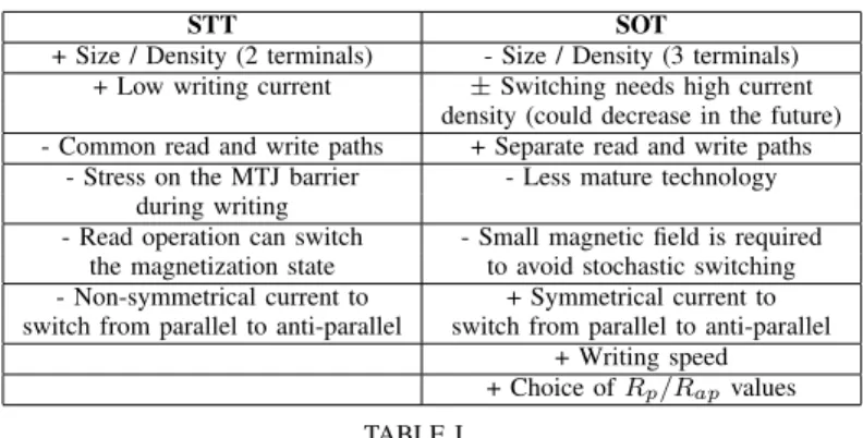
STT SOT
+ Size / Density (2 terminals) - Size / Density (3 terminals) + Low writing current ± Switching needs high current
density (could decrease in the future) - Common read and write paths + Separate read and write paths
- Stress on the MTJ barrier - Less mature technology during writing
- Read operation can switch - Small magnetic field is required the magnetization state to avoid stochastic switching - Non-symmetrical current to + Symmetrical current to switch from parallel to anti-parallel switch from parallel to anti-parallel
+ Writing speed + Choice of Rp/Rapvalues
TABLE I
COMPARATIVE TABLE OFSTTANDSOT
a ferromagnetic material with a majority of ”spin up” the electrons with a ”spin down” are slowed, stopped or even reflected, allowing only the electrons with an ”spin up” to pass through the material. This means that depending on the majority spin, a ferromagnetic material can be more or less resistive, this is called the Magnetoresistance effect.
The central device of all MRAMs today is the MTJ, which is based on the Tunnel Magnetoresistance effect (TMR) and which is intrinsically immune to radiations [11]. The MTJ is composed of two ferromagnetic layers, a reference layer (with a fixed magnetisation) and a storage layer (with a freely imposable magnetisation) with a thin insulator (barrier) between them. Depending on the relative magnetic orientation of the two layers (parallel or anti-parallel) the structure resistance changes being either high or low. This is caused by the electrons being able to pass more or less easily through the device and the thin insulator. Fig. 3 shows a simplified structure of the MTJ [12]. Changing the magnetic orientation of the storage layer makes it possible to have the MTJ in two different states: Parallel, or Anti-parallel. Depending in which state the MTJ is in, it has a different resistance Rp (parallel) or Rap (anti-parallel) [10].
Today the two main switching techniques that are either on the way of being integrated into industrial products or that have a large potential are respectively, Spin Transfer Torque switching (STT) and Spin Orbit Torque switching (SOT). The SOT process is still in the early stages of development. STT switching uses a polarized current injected through the 2-terminal MTJ to switch the magnetization of the storage layer [13]. Where as SOT uses a current passing under the storage
Fig. 3. (a) Simplified structure of a Magnetic Tunnel Junction: Right Parallel (Rp), Left Anti-parallel (Rap); (b) STT-MTJ (Spin Transfer Torque); (c)
Fig. 4. Example of material redundancy: (a) TMR (Triple Modular Redun-dancy), (b) DMR (Dual Modular Redundancy).
layer of the 3-terminal MTJ, in a conducting line [14] (Fig. 3). Table 1 summarizes the main pros and cons of both STT-MTJ and SOT-STT-MTJ. For instance SOT has separate reading and writing paths leading to high reliability and very high endurance, while STT share the same path. On the other hand STT with its 2-terminal structure is smaller than SOT that has 3-terminals.
D. Hardening by design
In addition to the means of protection against radiation described above, it is possible to adopt a system level approach through redundancy, error detection and correction, or data scrubbing.
This can be done either materially or by software. The mate-rial redundancy method is the replication of system resources. The most commonly used method is TMR (Triple Modular Redundancy) that enables the detection and correction of errors [15], but DMR (Dual Modular Redundancy) [16] has also attracted the attention of designers because it requires only one replication of the system (Fig. 4). However it permits only the detection and not the correction of errors. Software redundancy [17] is a sequential execution of a same task followed by a vote. This results in a loss of performance without the material part of the application being modified. Data scrubbing is the periodic inspection of memory cells looking for errors. If errors are detected, they are corrected using redundant data [18].
E. Radiations
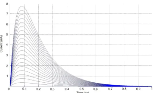
Even thought space is an empty place, there is in reality hundreds of thousands of energetic particles of various kinds (Protons, Heavy ions, Electrons) [19] that are mainly produced by the sun. In our study we chose to simulate the effect of heavy ions since they are one of the most energetic and dangerous particles for electronic circuits orbiting the earth [20]. By studding the effect of heavy ions we cover the effect of the other particles which have lower energies. Heavy ions are produced by solar wind or flares and have energies from a few keV to 10M eV (Fig. 5).
We simulate the heavy ions effect by a current pulse that is determined by the following equation [21]:
Iinj= Qinj τ1− τ2 (e−tτ1 − e −t τ2)
Where Qinj is the charge in Coulombs of a particle that
vary from -2pC to 2pC, τ1 and τ2 are material dependant
Fig. 5. Particle concentration and energies around the earth.
constants, here respectively 150ps and 50ps (which are the values of deposit and evacuation of electrical charges brought by a radiative particle). Fig. 6 gives a few plotted curves of the equation for several values of Qinj.
The effect of a heavy ion hitting a transistor has been documented in the past and has shown that the most sensitive strike location of a transistor is the drain [22] (Fig. 8). In our simulations we consider the worst case: we inject particles that have energies at the limit of what is potentially destructive and consider that all the particles hit the drains of the transistors.
III. CMOSCHARACTERISTIC’S FOR RADIATION HARDENING
This study has for objective to determine the performance of asynchronous logic in a harsh radiative environment using very advanced processes compared to synchronous logic (FD-SOI). We designed two memory elements of synchronous and asynchronous design. A flip-flop and a half-buffer for respectively synchronous and asynchronous design techniques. These two structures conduct the same role in the two worlds and were designed to have the same timing characteristics so they could be compared coherently.
All simulation results presented in this paper were run with Spectre electrical simulator under Cadence Analog Design Environment platform using the 28nm FD-SOI technology from ST Microelectronics.
Fig. 6. Examples of the induced current pulses generated by a particle impact waveforms simulated.
Fig. 7. Examples of transients measured for different ion strike locations along the source drain axis of a 0.25 µm bulk transistor. The gate length is 0.25 µm and the transistor width is 25 µm. [22]
A. Particle injection
To simulate the effect induced by a particle hitting the drain we inject a current pulse which has the same characteristics as a heavy ion strike to the drain of a transistor (Fig. 8). This current pulse will be sequentially injected in all the sensitive nodes of the evaluated circuit to determine the global sensitivity of the circuit. A sensitive node being any internal node except nodes connected to the supply voltage, ground, or any of the inputs or outputs.
B. Influence of the supply voltage
We conducted simulations of particle strikes at different supply voltages. From the simulations we have observed the inverse relationships between supply voltage and the amplitude on the induced pulse. In other words, as we increased the supply voltage for different particle strikes with identical energies, the effect of the particles decreased. This can be explained by the fact that, as the supply voltage increases the conductance of the transistor increases and also eases the dissipation of external energies.
C. Impact of the threshold voltage
In the 28nm FD-SOI design kit we have the choice between LVT (Low V t) and RVT (Regular V t) transistors. In our initial hypothesis RVT transistors would be more robust to pulses induced by particles strikes than LVT because of their superior V t, thus less sensitive to commutations. The simulation results demonstrated that LVT are finally more robust. This can be explained by the fact that LVT transistors have a higher leakage current than RVT, so the induced current pulses are evacuated quicker due to the lower resistance.
Fig. 8. Example of a particle injection (current pulse) in an OR gate.
Fig. 9. Graphical representation of the number of particles induced errors depending on the Body Biasing.
D. Influence of body biasing
FD-SOI enables us to use body biasing to play around with the V t of transistors. We then looked at the influence of vbb (body biasing voltage) in the case of particle induced errors. In RVT transistors, as vbb increased (boost configuration, V t decreases) the global number of errors induced by heavy ion strikes on the circuit decreased. As the transistors response is boosted the accumulated charges caused by particle strikes can be evacuated quicker. Concerning LVT transistors, being already more robust to particles than RVT, increasing or decreasing vbb has no further effect on them (Fig. 9).
IV. THE EFFECT OF NON-VOLATILITY IN A SIMPLE STRUCTURE
The next step in our study was to see how the introduction of MTJs in the half-buffer and flip-flop would affect their robustness towards particle strikes.
A. Non-volatile Flip-Flop
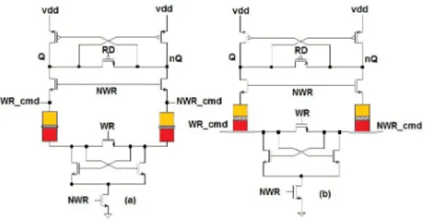
To design a non-volatile (NV) flip-flop we used the classic flip-flop from the previous section and replaced one of the latches with a NV latch. We chose to use a dual MTJ Latch cell (Hass) for its robustness towards radiation [23]. Fig. 10 shows the architecture used for both STT and SOT NV latches. During the writhing phase the MTJs are disconnected from the rest of the circuit with W R = 1 (N W R = 0), this allows the write command signal (W R cmd) to transit through the junctions in opposite directions thus writhing the two MTJs in opposite magnetic states. Reading is achieved by the RD signal. When RD is high Q and nQ are forced to the same value ( about vdd/2), and since the resistances of the MTJs are different, the latch becomes unstable and unbalanced, forcing Q to GN D or V DD depending on the state of the MTJ, and NQ to V DD or GN D.
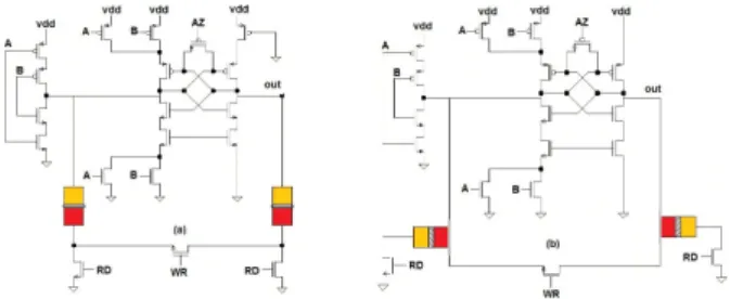
Fig. 11. Non-volatile C-element: (a) STT version, (b) SOT version
B. Non-volatile Half-Buffer
The design of a NV half-buffer was achieved by replacing the C-elements by NV C-elements previously designed in our laboratory [24]. Fig. 11 show the architecture used for both STT and SOT NV C-elements.
The reading and writing functionality for the MTJs are the same as described for flip-flops in the previous subsection.
C. Simulation results
Current pulses were injected into sensitive nodes as de-scribes earlier (Fig.8). Depending on the simulated circuit (volatile/non-volatile, synchronous/asynchronous) the number of sensitive nodes varies from 15 to 24. For each sensitive node we conducted successive simulations for all the possible input combinations, this lead to around 2000 individual simulations. The outputs of the flip-flop and half-buffer as well as the Magnetic states of the MTJs where compared to simulation results previously obtained without error injection using SOT-MTJ and STT-SOT-MTJ compact models described in Verilog A language [25].
Simulation results showed that due the high energies involved in some particles strikes, an error induced by a particle could write or even destroy an MTJ depending on where the particle hits. Some work have shown [11] that MTJs are robust against radiations, but like integrated circuit, it is the CMOS transistors that are sensitive towards particle strikes and indirectly causes bit flip on MTJ memory cells. Indeed, the current generated is high enough during a non-negligible time to induce such a behaviour. Moreover, an important thing to keep in mind when designing a circuit for radiative environments is the size of the transistors. The bigger the transistors are the less a particle hit will effect it and its surroundings. This can be explained by the fact that as transistors get bigger their resistance decreases, thus the amplitude of the voltage created by the current pulse will be lower.
To render MTJ more robust to radiative environment a solution is to increase there dimensions:
1) Influence of the MTJs dimensions for STT: As the dimensions of the MTJ increases more current is needed to write the junction. This is explained by the resistance of the MTJ decreasing as its size increases.
Circuit type Number of Errors Flip-Flop 0.41 NV STT Flip-Flop 0.47 NV SOT Flip-Flop 0.43 Half-Buffer 0.35 NV STT Half-Buffer 0.82 NV SOT Half-Buffer 0.66 TABLE II
COMPARATIVE TABLE OFSYNCHRONE/ASYNCHRONE, VOLATILE/NON-VOLATILE ANDSTT/SOT
2) Influence of the strip dimensions for SOT: The switching mechanism for SOT-MTJs is dependant on the current density that passes under the junction in the conduction line. If the dimension of the conduction line are increased the current density that passes under the junction for a same given current will be lessened. Thus increasing the dimensions until a point where the current pulses induced by particles strikes will not create a sufficient current density under the junction to write the junction its a way of increasing is robustness.
D. Results and Interpretation
The inclusion of MTJ in the flip-flop or half-buffer has not rendered them more robust to particles strikes. This can be explained in the following manor: The addition of non-volatility in an elementary circuit increases the number of sensitive nodes as well as the global complexity. The more sensitive nodes the more a circuit is sensitive to errors induced by particles.
Table II gives a synchrone/asynchrone, volatile/non-volatile and STT/SOT comparison to particles strikes. The number of errors is determined by the actual number of errors visualised at the circuits outputs and/or Magnetic states. These numbers are normalised to the number of inputs and sensitive nodes so as to have a coherent comparison. The junctions used had a writing stripe of 200nm × 100nm × 5nm for SOT and diameter of 40nm for both STT and SOT. The energy needed to write such an STT-MTJ with a current pulse of 44µA/2.7ns is 0.15pJ . This energy is twice as less than the energy needed for the flip-flop to change its output (0.3pJ ). To render the junction more robust towards particle strikes, the MTJ switching energy should be increased. This can be done by increasing the dimensions of the MTJ or through customising the magnetic post-process.
We can see that volatile half-buffer is very slightly more ro-bust than volatile flip-flop, and the addition of MTJs decreases there robustness. We can also see that SOT is also very slightly more robust than STT. This is due to the writing strip, more current is needed to write the junction so it is less sensitive than STT. The NV half-buffer is a lot less robust than the NV flip-flop. This can be explained because the Hass structure used in the flip-flop is the most robust architecture compared to a classical half buffer structure which is composed of two NV Muller cells each one having two differential MTJs.
V. GENERALCONCLUSION AND PERSPECTIVES
This work has allowed us to fully understand the influence of heavy ion strikes on transistors in elementary circuits. We have seen the influence of the supply voltage and body biasing on both LVT and RVT transistors when confronted with particle strikes. The simulation results have demonstrated that using the highest supply voltage permitted by the technology, in conjunction with LVT transistors is the best option to harden a system at transistor level. We also investigated the influence of MTJ in elementary circuits. The integration of MTJs in elementary circuits is not the solution to harden circuits even tough they are intrinsically immune to radiation. There integration at an architectural level with standard structures to limit the number of sensitive nodes could be the solution. Concerning the differences between synchronous and asynchronous design, it is difficult to determine which is more robust at transistor level. The differences are based on the communication protocols, the robustness of one design method over the other should become visible in a more complex architecture such as a pipeline structure.
Our next step will be to compare both asynchronous and synchronous architectures in a pipeline to see how the errors are propagated through the different stages; this should give us an in-depth comparison of both asynchronous and synchronous design towards radiative environments. This will lead to a study on hardening techniques by design such as DMR (Dual Modular Redundancy) and TMR (Triple Modular Redun-dancy). Indeed, the use of non-volatility thanks to MTJs should allow the restoration of secure data after a particle strike. This will allow us to compare both synchronous and asynchronous architectures in new conditions to determine which is more robust in harsh radiation environments. We will then evaluate a one MTJ one resistor rather than a two MTJ structure to see the difference in behaviour. Flowed by a study of the Mean Time To Failure (MTTF) of all the different combinations of volatile/non-volatile, synchronous/asynchronous. Finally we will investigate the hardening of MTJs by customisation, either at design or process level.
ACKNOWLEDGMENT
We would like to thank the CEA and CNES for their financial support for this work.
REFERENCES
[1] Renaudin, Marc and Rigaud, Jean Baptiste, Etat de lart sur la conception des circuits asynchrones: perspectives pour lint´egration des syst`emes complexes, rapport de recherche interne TIMA/STMicroelectronics, 2000.
[2] Vivet, Pascal, Une m´ethodologie de conception de circuits int´egr´es quasi-insensibles aux d´elais: application `a l’´etude et `a la r´ealisation d’un processeur RISC 16-bit asynchrone, Ph.D. thesis, Institut National Polytechnique de Grenoble-INPG, 2001.
[3] Moreira, Matheus Trevisan and Calazans, Ney Laert Vilar, Proposal of an Exploration of Asynchronous Circuits Templates and their Applica-tions, 2014.
[4] Jeitler, Marcus and Lechner, Jakob, Comparing the robustness of syn-chronous and asynsyn-chronous circuits by fault injection, 2009.
[5] Muttersbach, Jens and Villiger, Thomas and Fichtner, Wolfgang, Prac-tical design of globally-asynchronous locally-synchronous systems, Ad-vanced Research in Asynchronous Circuits and Systems, 2000.(ASYNC 2000) Proceedings. Sixth International Symposium on, pp. 52-95. [6] Teehan, Paul and Greenstreet, Mark and Lemieux, Guy, A survey and
taxonomy of GALS design styles, Design & Test of Computers, IEEE, 2007, vol. 24, no 5, pp. 418-428.
[7] Roche, Philippe and Autran, Jean-Luc and Gasiot, Gilles and Munteanu, Daniela, Technology downscaling worsening radiation effects in bulk: SOI to the rescue, Nuclear Science, IEEE international electron device meeting (IEDM2013). Washington DC, 2013, pp. 766-769.
[8] Flatresse, Philippe and Giraud, Bastien and Noel, J and Pelloux-Prayer, Bertrand and Giner, Fabien and Arora, D and Arnaud, Franck and Planes, Nicolas and others, Ultra-wide body-bias range LDPC decoder in 28nm UTBB FDSOI technology, Solid-State Circuits Conference Digest of Technical Papers (ISSCC), 2013 IEEE International, 2013, pp. 424-425. [9] Kang, Wang and Zhao, Weisheng and Wang, Zhaohao and Klein, Jacques-Olivier and others, Dafin´e and Chappert, Claude, An overview of spin-based integrated circuits, ASP-DAC, 2014, pp 676-683. [10] Di Pendina, Gregory, Conception innovante et d´eveloppement d’outils
de conception d’ASIC pour Technologie Hybride CMOS/Magn´etique, Universit´e de Grenoble, 2012.
[11] Conraux, Yann, Pr´eparation et caract´erisation d’un alliage amorphe ferrimagn´etique de GdCo entrant dans la conception de jonctions tunnel magn´etiques R´esistance des jonctions tunnel magn´etiques aux rayon-nements ionisants, Ph.D., Universit´e Joseph-Fourier-Grenoble, 2005. [12] Sousa, Ricardo C and Prejbeanu, I Lucian, Non-volatile magnetic
random access memories (MRAM), Comptes Rendus Physique, 2005, vol. 6, no 9, pp. 1013-1021.
[13] Dieny, Bernard and Sousa, RC and Herault, J and Papusoi, C and Prenat, G and Ebels, U and Houssameddine, D and others, Spin-transfer effect and its use in spintronic components, International Journal of Nanotechnology, 2010, vol. 7, no 4, pp. 591-614.
[14] Jabeur, K and Buda-Prejbeanu, LD and Prenat, G and Di Pendina, G, Study of two writing schemes for a magnetic tunnel junction based on spin orbit torque, International Journal of Electronics Science and Engineering, 2013, vol. 7, no 8, pp. 501-507.
[15] Di, Jia, A framework on mitigating single event upset using delay-insensitive asynchronous circuits, Region 5 Technical Conference, 2007 IEEE, 2007, pp. 354-357.
[16] Gong, Rui and Chen, Wei and Liu, Fang and Dai, Kui and Wang, Zhiying, A new approach to single event effect tolerance based on asynchronous circuit technique, Journal of Electronic Testing, 2008, vol. 24, n 1-3, pp. 57-65.
[17] Bolchini, Cristiana and Miele, Antonio and Rebaudengo, Maurizio and Salice, Fabio and Sciuto, Donatella and Sterpone, Luca and Violante, Massimo, Software and hardware techniques for SEU detection in IP processors, Journal of Electronic Testing, 2008, vol.24, no 1-3, pp.35-44. [18] Goncalves, Olivier.Conception sur mesure d’un FPGA durci aux radia-tions base de mmoires magntiques. Ph.D. thesis, Universit´e de Grenoble, 2013.
[19] Peronnard, Paul, M´ethodes et outils pour l’´evaluation de la sensibilit´e de circuits int´egr´es avanc´es face aux radiations naturelles, Ph.D. thesis, Universit´e Joseph-Fourier-Grenoble I, 2009.
[20] Robert C. Baumann, Soft Errors in Advanced Semiconductor Devices -Part I: The Three Radiation Sources, Device and Materials reliability, IEEE Transactions on, 2001, vol.1, no 1, pp.17-22.
[21] Zhao, Weisheng and Deng, Erya and Klein, Jacques-Olivier and Cheng, Yuanqing and Ravelosona, Dafin´e and others, A radiation hardened hy-brid spintronic/CMOS nonvolatile unit using magnetic tunnel junctions, Journal of Physics D: Applied Physics, 2014, vol.47, no 40, pp. 405003. [22] Ferlet-Cavrois, V and Paillet, P and Gaillardin, M and Lambert, D and Baggio, J and Schwank, JR and Vizkelethy, and others, Statistical analysis of the charge collected in SOI and bulk devices under heavy lon and proton irradiationImplications for digital SETs, Nuclear Science, IEEE Transactions on, 2006, vol. 53, no 6, pp. 3242-3252.
[23] Raphael Martins Brum, Une tude des mmoires magnetiques appliques aux processeurs et FPGAs, Ph.D. thesis, Universit´e Montpellier 2, 2014. [24] Zianbetov, Eldar and Beigne, Edith and Di Pendina, Gregory, Non-Volatility For Ultra-Low Power Asynchronous Circuits in Hybrid CMOS/Magnetic Technologys, 2015.
[25] http://www.mos-ak.org/grenoble 2015/presentations/T5 Bernard-Granger MOS-AK Grenoble 2015.pdf.