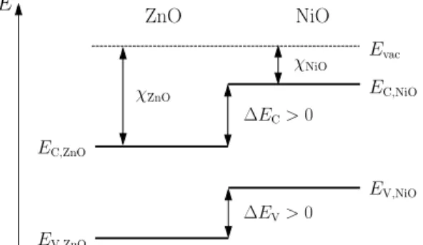
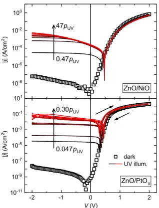
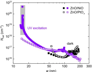
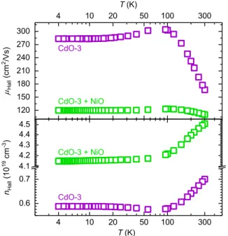
Nickel Oxide–Based Heterostructures with Large Band Offsets
Texte intégral
Figure
Documents relatifs
(i) the saturation magnetization 4πM S at room temperature is equal to 1700 G, close to the bulk value, (ii) the magnetization curves are isotropic in the film plane, and (iii) the
Van Vleck, The Theory of Electric and Magnetic Susceptibilities, Oxford University Press (1932) p.. Rietveld XPD analysis result data for the samples obtained by
L’archive ouverte pluridisciplinaire HAL, est destinée au dépôt et à la diffusion de documents scientifiques de niveau recherche, publiés ou non, émanant des
Nickel oxide is a p-type semiconductor, is an important material because of its large direct optical gap between 3.6 and 4.0 eV; and easy to deposit in thin layers by many
Abstract: In this work, thin films of nickel oxide (NiO) were deposited by a simple and inexpensive technique, which is spray pyrolysis on ordinary glass substrates heated to a
L’archive ouverte pluridisciplinaire HAL, est destinée au dépôt et à la diffusion de documents scientifiques de niveau recherche, publiés ou non, émanant des
The best matching of the distributions obtained at various temperatures was obtained with ~toN~ = 2.5 x 10~~ (cmvs)~~, a value twice lower than that given by multiplying the
Numerical modeling of the L-Band emission and scattering of a rough soil layer covered with a grass litter layer- consideration of Moisture and Temperature gradients..
