HAL Id: hal-02137915
https://hal.archives-ouvertes.fr/hal-02137915
Submitted on 23 May 2019
HAL is a multi-disciplinary open access
archive for the deposit and dissemination of
sci-entific research documents, whether they are
pub-lished or not. The documents may come from
teaching and research institutions in France or
abroad, or from public or private research centers.
L’archive ouverte pluridisciplinaire HAL, est
destinée au dépôt et à la diffusion de documents
scientifiques de niveau recherche, publiés ou non,
émanant des établissements d’enseignement et de
recherche français ou étrangers, des laboratoires
publics ou privés.
To cite this version:
Philippe Chiquet, Maxime Chambonneau, V. Della Marca, Jérémy Postel-Pellerin, Pierre Canet, et
al.. Phenomenological modelling of non-volatile memory threshold voltage shift induced by nonlinear
ionization with a femtosecond laser. Scientific Reports, Nature Publishing Group, 2019, 9 (7392),
�10.1038/s41598-019-43344-x�. �hal-02137915�
www.nature.com/scientificreports
phenomenological modelling of
non-volatile memory threshold
voltage shift induced by nonlinear
ionization with a femtosecond laser
philippe Chiquet
1, Maxime Chambonneau
2, Vincenzo Della Marca
1, Jérémy
postel-pellerin
1, pierre Canet
1, sarra souiki-Figuigui
1, Guillaume Idda
1, Jean-Michel portal
1&
David Grojo
2the behaviour of semiconductor materials and devices subjected to femtosecond laser irradiation has been under scrutiny, for many reasons, during the last decade. In particular, recent works have shown that the specific functionality and/or geometry of semiconductor devices, among which non-volatile memory (NVM) devices hold a special place, could be used to improve the knowledge about ultrafast laser-semiconductor interactions. so far, such an approach has been applied to draw conclusions about the spatio-temporal properties of laser propagation in bulk materials. Here, by comparing the evolution of the electrical characteristics of Flash cells under the cumulative effect of repeated femtosecond laser pulses with first-order physical considerations and TCAD (Technology Computer Aided Design) simulations, we clearly establish the role of the carriers created by nonlinear ionization on the functionality of the structures. the complete electrical analysis informs indirectly on the energy of the laser-produced free-carriers which, to date, was almost inaccessible by an experimental method applicable to the bulk of a material. establishing the link between the carrier energy and laser parameters is of major importance to improve the comprehension of the nonlinear ionization mechanisms associated to intense laser-semiconductor interactions and applied in various fields from microelectronics to laser micromachining.
One of the important reasons for which the laser/semiconductor interaction has been investigated during the last two decades lies in the increasing importance of single-event effects (SEE) occurring in nowadays electronic circuits. In particular, single-event upsets (SEU), defined as the flips of a logical state or transient changes of an electrical parameter, occur when said circuits are exposed to energetic particles in radiative environments. Such systems should ideally be tested with the help of particle accelerators, but this solution remains both costly and impractical. In order to emulate the effect of energetic particles such as heavy ions while avoiding the associated radiation damage that comes with it, an alternative solution consists in generating charge carriers in circuits or individual components by irradiating them with laser beams1,2. The development of nonlinear optics has shown
that the spatial and temporal evolutions of the density of carriers generated through laser irradiation is ruled by equations dependent on In, where I is the intensity of the laser beam at a given wavelength and n is the number
of absorbed photons required to generate a single free electron-hole pair in the semiconductor3–8. As a direct
consequence, carrier generation in (nonlinear) modes such as n > 1 is characterized by a carrier density which is spatially confined near the focus of the laser beam, allowing to target specific locations in a component or a circuit as long as his characteristic dimensions remain larger than the laser spot size. Since the feasibility of through-wafer two-photon absorption resulting from femtosecond laser irradiation has been demonstrated9,10,
transient and charge collection measurements performed on semiconductor devices such as bipolar transistors, Fin Field-effect transistors (FinFETs), and diodes have been compared to numerical simulations in order to be able to emulate and further understand SEEs thanks to this method11–17. Our recent works have shown that the
peculiarities of other semiconductor devices, such as Flash memory cells, can be used as a way to characterize the
1Aix-Marseille University, CNRS, IM2NP, F-13397, Marseille, France. 2Aix-Marseille University, CNRS, LP3, F-13288,
Marseille, France. Correspondence and requests for materials should be addressed to P.C. (email: philippe.chiquet@ im2np.fr)
Received: 14 January 2019 Accepted: 16 April 2019 Published: xx xx xxxx
carriers generated by femtosecond laser irradiation in semiconductors18,19. Flash memory cells can be described,
as depicted in Fig. 1, as regular Metal-Oxide-Semiconductor (MOS) transistors on which a multi-layered oxide (generally a SiO2/Si3N4/SiO2 tri-layer) and an additional control gate (CG) have been added. The threshold
volt-age Vt of the device can be modulated according to the amount of charge QFG stored in the floating gate (FG), and
both electrical quantities can be linked by the following relationship: = − Vt Vt Q C (1) FG ONO 0
where Vt0 and CONO are respectively the neutral threshold voltage (i.e. the particular Vt value for which QFG = 0)
and the capacitance of the FG/ONO/CG stack. According to the sign of QFG, the floating gate transistor can be
driven into two distinct and stable logical states (“erased” when QFG > 0 and “programmed” when QFG < 0).
The floating gate charge variation necessary for the device to switch from one state to the other is assured when electron transit through the tunnel oxide is enabled by the application of suitable electric signals to the various terminals of the transistor. Flash cells are generally programmed via injection of hot electrons into the floating gate, and erased when electrons are withdrawn from the floating gate through Fowler-Nordheim conduction20–25.
We have recently shown that femtosecond laser irradiation of initially programmed and erased Flash cells could provoke their progressive shifting towards the opposite electrical state18,19. As the biasing conditions of the
cells were neither compatible with hot carrier injection nor with Fowler-Nordheim conduction during the laser shots, charge carrier transit through the injection zone, for laser energies below the threshold for irreversible device degradation, was attributed to the tunneling of energetic carriers created in the substrate and the floating gate.
The present article completing these previous studies deals with the modelling of the ultrafast laser-induced shift of the threshold voltage. By varying the laser intensity, it is found that the laser-induced programming speed of Flash memories can be controlled. Additionally, the asymptotical logical state of the irradiated devices can be adjusted by applying a bias voltage on the control gate. A good agreement is found between the experiments and first-order physical considerations as well as Technology Computer Aided Design (TCAD) simulations, which both enable us to access to the laser-produced free carrier dynamics. The whole set of results enhance the global understanding of the femtosecond laser-transistor interaction and demonstrates the possibility to impact single isolated Flash memories with light.
Results and Discussion
electrical behaviour of the injection zone during femtosecond laser irradiation.
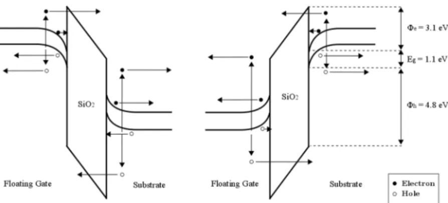
Backside femto-second laser irradiation, after altering the p-doped silicon substrate of the Flash cells, reaches the n-doped silicon floating gate with a diminished intensity after successive reflections on both silicon/oxide interfaces. During a given laser pulse, the strength and orientation of the vertical electric field reigning in the injection zone are deter-mined by QFG and the voltages applied to the terminals of the transistor, as depicted in Fig. 2. Due to the nature ofthe experiments led in this study, and in particular the fact that no measurement configuration will involve a non-zero value of VD, the norm of the vertical oxide field can be considered as constant in the longitudinal direction
(i.e., across the transistor channel located between the source and the drain).
Electron-hole pairs are generated in both electrodes with two-photon ionization, which is the dominant mechanism for carrier production in silicon at the considered wavelength of 1300 nm9. According to the
ori-entation of the field, as shown in Fig. 2, electrons and holes, whether they result from laser irradiation or were already present in the silicon at thermodynamic equilibrium, can flow into (or get extracted from) the floating gate through the tunnel oxide with a non-zero probability.
This basic model, in the light of which the subsequent experimental results will be interpreted, also relies on a few assumptions backed up by physical considerations or results discussed in our previous studies18,19. More
spe-cifically, it will be considered that femtosecond laser irradiation will not affect the electrical properties of the tun-nel oxide because of the high value of the SiO2 bandgap (around 9 eV) that would require ten-photon absorption
to come into play for laser energy deposition at 1300-nm wavelength. Briefly, the theoretical scenario describing the behaviour of Flash memory device irradiated by ultrashort laser pulses relies on the tunneling of free electrons
Figure 1. (a) Schematic representation of a standard Flash memory cell. (b) Electrical equivalent model of a
standard Flash memory cell displaying the terminals of the floating gate transistor (control gate – CG, source – S, bulk – B, drain – D).
www.nature.com/scientificreports
www.nature.com/scientificreports/
through the oxide layer of the cell before the electron-hole pairs potentially recombine in a few ns26. Depending
on the migration of these free electrons produced by two-photon ionization, the net charge of the floating gate is changed by this way. One must emphasize that the employed low repetition rate of 1 kHz ensures no thermal/ electron accumulation on a pulse-to-pulse basis. In other words, the electron-hole pairs created by one pulse have recombined when the following pulse irradiates the cell. It can thus be concluded that the only consequence of individual laser shots, after thermodynamic equilibrium is reached again, lies in a change of the floating gate charge and the potential distribution in the vertical direction of the injection zone. In our previous works18,19 no
damage of the tunnel oxide (surface or volume) has been observed, even at laser energies much higher than the ones employed in this study. This can indicate the effect of Anode Hole Injection (AHI) can here be neglected, especially since the biases applied on the Control Gate (and thus on the Floating Gate) are low. Moreover, the barrier height seen by holes from the substrate is higher than the one seen by electrons from the Floating Gate (4.8 eV and 3.1 eV respectively), thus considerably reducing their injection probability.
experimental results.
In our experiments, the laser pulse energy was adjusted but ultimately, the inten-sity I is the parameter enabling the direct evaluation of the electron deninten-sity ne during laser irradiation. Due tothe extremely low absorption coefficient at 1300-nm wavelength (α = 4.5 × 10⁻⁵ cm−1), the intensity transmitted
through 1 mm of silicon is >99.9% of the input intensity, according to Beer-Lambert law27. Therefore, the
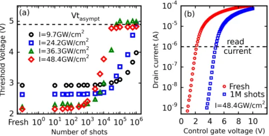
absorp-tion of the material at this wavelength is negligible. The associated transmission coefficient can thus be calculated using Fresnel equations at normal incidence and the intensity in the vicinity of the cell can be easily obtained by measuring the intensity in air and multiplying it by the transmission coefficient T = 69.1%. Nonlinear propaga-tion phenomena could theoretically limit the energy deposipropaga-tion in the vicinity of the cell. However, due to the extremely low energy values (a few hundreds of pJ) employed in our study, these phenomena have been shown to be negligible3. A typical experimental acquisition of the threshold voltage Vt as a function of the number of
laser shots for initially erased cells at VCG = 0 is displayed in Fig. 3a. These results show that the erased cells are
gradually programmed after cumulative laser shots as Vt evolves according to a “S-shaped” curve within this semi-logarithmic plot. One can note that the starting point is different for each dataset due the different erased threshold voltage values (between 2 and 3 V) of the tested cells. While the asymptotic threshold voltage Vtasympt
remains the same in each case, it can be observed that increasing the laser pulse intensity I accelerates the evolu-tion of Vt, which reaches its final value after fewer laser shots. This is consistent with the dependence of the num-ber of laser-produced free carriers with two-photon absorption. Drain current characteristics retrieved during
reading operations before laser irradiation and after 106 laser shots (I = 48.4 GW/cm2) are shown in Fig. 3b. The
measured Id(VCG) characteristic is merely shifted to the right under laser irradiation and is not subject to
defor-mations that are often taken as experimental evidence of device degradation, whether resulting from electrical stress or laser-related deterioration18,28. Further experiments show that this result is valid for laser intensities up
to about 110 GW/cm2 and that, at least in the 9.7–48.4 GW/cm2 range investigated in the present work, this shift
can most likely be solely explained by the charging of the floating gate with charge carriers transiting through the tunnel oxide, which is compatible with the model described above.
Modelling the threshold voltage evolution with the number of laser shots.
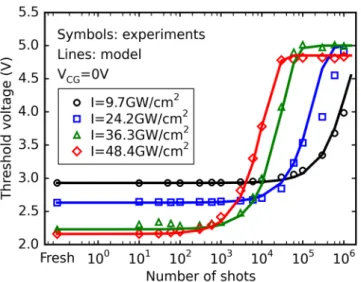
The experiment described in the above section has then been carried out (I = 48.4 GW/cm2) for both initially erased andpro-grammed Flash cells biased by several control gate voltage values. The resulting “S-shaped” curves, displayed in Fig. 4 (markers), show that the asymptotic threshold voltage differs according to the VCG value applied to
the device. In particular, the application of a sufficiently negative VCG value on initially erased cells leads to a
threshold voltage evolution contrary to the one monitored in the VCG = 0 V case (and vice-versa for initially
programmed cells). The experimental “S-shaped” curves, can be modelled using a generalized sigmoid function of the following form:
Figure 2. Band diagram of the injection zone of the Flash cell (i.e. electron energy as a function of vertical
position in said zone) represented for both possible directions of the vertical electric field. Vertical arrows indicate the creation of electron-hole pairs in both electrodes under laser irradiation, while the horizontal arrows depict the motion of free electrons (plain circles) and holes (empty circles), whether laser-generated or not, under the influence of the electric field. The physical quantities Eg, φe and φh are respectively the silicon
= + + − V n A B e ( ) 1 (2) t Cn
where A, B and C are three fitting constants, and n the number of applied laser shots.
Knowing the two extremal threshold voltage values Vtstart and Vtasympt (i.e., when n = 0 and n → ∞ in the
equa-tion above) through electrical characterizaequa-tion, expressions for A and B can be derived by solving a two-equaequa-tion system, and Eq. (2) finally becomes:
= − + − + − Vt n Vt Vt V Vt V Vt e ( ) 2 ( ) 2( ( ) ) 1 (3)
start asympt CG asympt CGCn start
The fitting curves (full lines) obtained with this model for erased and programmed cells are consistent with the experimental results displayed in Fig. 4 for a well-chosen value of parameter C which is independent of the applied control gate voltage (C = 1.5 × 10⁻⁴ ± 0.5 × 10⁻⁴ for all the curves). These results thus demonstrate that,
when the laser intensity is low enough to avoid device degradation, it is possible to limit or enhance the laser effect by applying a suitable control gate bias and that the resulting evolution of the threshold voltage can be predicted by relatively simple means.
The model has then been used to fit the set of data previously displayed in Fig. 3a and reproduced in Fig. 5. The values of the growth rate C used to reproduce the experimental curves are listed in Table 1 and displayed in Fig. 6
as a function of I. It can be observed that C exponentially increases with laser intensity in the 9.7–48.4 GW/cm2
range, and can thus be written as:
Figure 3. (a) Evolution of experimental Vt of erased cells as a function of the number of laser shots at different
intensities (VCG = 0 V). (b) Evolution of the drain current as a function of the control gate voltage before and
after 1 million laser shots at 48.4 GW/cm2.
Figure 4. Evolution of Vt of (a) initially erased and (b) initially programmed memory cells, as a function of the
www.nature.com/scientificreports
www.nature.com/scientificreports/
≈ C C exp I I (4) 0 0with C0 = 4.6 × 10⁻⁷ and I0 = 8.2 GW/cm2 as extracted from Fig. 6. The fact that C does not vary as I2, as could
be expected for a mechanism induced by two-photon ionization, shows that the number of free carriers cannot be the only explanation for the observed evolution of the threshold voltage under laser irradiation, but that their intensity distributions should play a large role as well.
An increase in the deposited energy per laser pulse will likely induce higher densities of laser-generated car-riers that are potential candidates to transit through the tunnel oxide3. Moreover, carriers created by two-photon
ionization, which remains the main electron generation process at 1300 nm in silicon in the femtosecond regime, can subsequently absorb additional photons via an inverse Bremsstrahlung process29,30 as long as the laser field is
present (during the pulse). This should result in generally more ‘heated’ energy distributions for the carriers, and thus a higher tunneling probability as the transmission coefficient for both electrons and holes can be expressed, thanks to the commonly used Wentzel–Kramers–Brillouin (WKB) approximation, as31–34:
Figure 5. Evolution of the threshold voltage shift of initially erased cells as a function of the number of laser
shots at different intensities and VCG = 0 V.
Laser intensity 9.7 GW/cm2 24.2 GW/cm2 36.3 GW/cm2 48.4 GW/cm2
C 1.4 × 10⁻⁶ 8.5 × 10⁻⁶ 5.0 × 10⁻⁵ 1.4 × 10⁻⁴
Table 1. Value of parameter C for different pulse intensities (VCG = 0 V).
ε = φ ε − − ⁎ T exp m heE ( ) 4 2 3 ( ) (5) triangle oxe h ox e h , , 3 2 ε = φ ε φ ε − − − − − ⁎ T exp m heE eE t ( ) 4 2 3 ( ) ( ) (6) trapeze oxe h ox e h e h ox ox , , 3 2 , 23 where m⁎
oxe h, and φe,h are respectively the SiO2 effective mass and the Si-SiO2 barrier height for electrons and holes
tunneling through the oxide, Eox is the norm of the oxide electric field, and ε the free-carrier energy with respect
to the bottom of the conduction band (electrons) or the top of the valence band (holes). According to its energy, a laser-generated carrier will either face a triangular or trapezoidal barrier, as seen in Fig. 7, which explains the need for two separate transmission coefficient expressions. The oxide electric field, for a tunnel capacitor submit-ted to a VFG − VB potential difference, can be written as35:
ψ ψ = = − − − + E V t V V V t ( ) (7) ox ox ox FG B FB S FG ox
where VFB is the flatband voltage of the capacitor, tox its oxide thickness, ψS and ψFG the surface potentials of the
substrate and floating-gate respectively.
Assuming a density of generated free electron-hole pairs in the 1019 cm−3 range in both electrodes for the
investigated laser intensities3, and assuming that a part of these carriers will be removed from each of the space
charge layers due to the reigning electric field, a carrier surplus will exist in each electrode compared to the ther-modynamic equilibrium case. Under these conditions and the reasonnable approximation of a metallic behaviour for both electrodes, the expression of the oxide electric field merely reduces to:
≈ − − E V V V t ( ) (8) ox FG B FB ox
This last equation, when combined with Eqs (5) and (6), allows a deeper understanding of the experimental results displayed in Figs 4 and 5. At a given laser intensity, and considering the fact that |VFG| = f(|VCG|) is an
increasing function (see supplementary material of our previous work19), the oxide electric field and thus the
transmission coefficient of tunneling electrons will be enhanced as |VCG| gets higher. These considerations should
explain why, as seen in Fig. 3 for both initially programmed and erased cells, a given threshold voltage value can be reached “faster” (i.e. a given amount of floating gate charge variation is achieved through fewer laser shots) for higher |VCG| values. Conversely, Fig. 5 shows the asymptotic threshold voltage can be reached faster, for a given
VCG value, when the laser intensity is increased. This acceleration can most likely be explained by the fact that,
as previously stated, an increase in I (and thus in energy) should lead to a general increase in ε and transmission coefficient for the laser-generated carriers. Looking back at the simulation results displayed in Table 1, this likely corresponds to a suitable physical explanation for the laser intensity dependence of the coefficient C introduced in Eq. (2).
Cancelling the laser effect on the flash cells and analytical derivation of the asymptotic voltage.
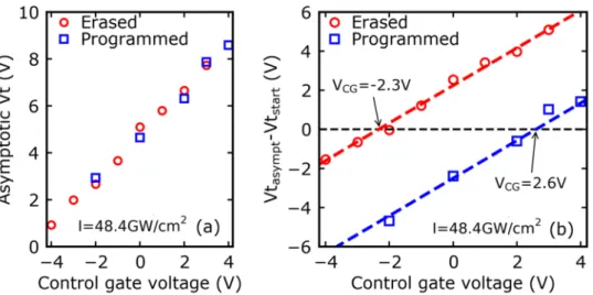
Previously in Fig. 4, it can be observed that for a certain control gate voltage the effect of the laser irradiation on the evolution of the threshold voltage can be cancelled. According to these measurements, this particular VCG
value, for Vt to remain constant should respectively be around −2 V and in the +2 V to +3 V range for initially
Figure 7. Upper part of the band diagram of the tunnel capacitor. According to the sign of Vox (and thus the
value of VCG), the role of the cathode can be either played by the floating gate (Vox < 0) or the substrate (Vox
> 0). Electrons with energies of ε1 and ε2 with respect to the bottom of the cathode conduction band ECc will
respectively meet a trapezoidal and triangular tunneling barrier. Lower part of the band diagram is omitted as tunneling of laser-generated free holes should hardly contribute to the variation of QFG due to the discrepancy
www.nature.com/scientificreports
www.nature.com/scientificreports/
erased and programmed cells. To investigate this matter, asymptotic values of the threshold voltage are shown in Fig. 8 as a function of the control gate voltage. Results displayed in Fig. 8a show that Vtasympt follows a linear
dependence with VCG with a slope equal to unity, so the asymptotic voltage can be expressed as:
= + = +
Vtasympt aVCG b VCG b (9)
where a and b are constants.
Moreover, one can observe that for a given VCG, laser irradiation leads to the same Vtasympt value for each
mem-ory cell, whatever its initial state. In other words, coefficients a and b should not depend on the initial quantity of charge stored in the Flash cell. According to Fig. 8b, the needed VCG values to cancel the effect of laser irradiation
in initially erased and programmed cells (i.e. Vtasympt − Vtstart = 0) are respectively −2.3 V and +2.6 V, which is
coherent with the above predictions. The physical significance of these two values has then been investigated with the help of Technology Computer Aided Design (TCAD) simulations whose results are displayed in Fig. 9.
The simulation of the electrical behaviour of the initially erased and programmed Flash cells show that, in both cases, the band diagram of the tunnel capacitor can be “flattened” when the VCG values extracted from Fig. 8b are
applied on the control gate. The threshold voltage remains constant because no net charge transit is possible through the tunnel oxide as the band diagram is flat, in accordance with19. Under the hypothesis that the Vt
asympt
is reached when the band diagram of the tunnel capacitor becomes flat, which has been demonstrated through the results presented in this section of the report, and considering the drain, source and bulk terminals to be grounded (VD = VS = VB = 0 V), we were able to derive in one of our previous works19 the following relationship:
Figure 8. Evolution of (a) the asymptotic Vt and (b) the shift Vtasympt – Vtstart as a function of the CG biasing
voltage (I = 48.4 GW/cm2) for initially erased and initially programmed cells.
Figure 9. (a) Distribution of the electric field across the tunnel oxide of an erased device and (b) band
diagrams of the injection zone obtained with TCAD simulation for different biasing conditions (VCG = 0 V and
= − − − + + − − + −
(
)
Vt n Vt V Vt V K V Vt Vt e ( ) 2 2 1 (12) start CG FB CG VK start Cn 0 0 FBKnowing the laser intensity dependence of C and since all the other physical quantities can be determined or set (VCG), the threshold voltage of the irradiated Flash cell can thus be predicted after any number of laser shots
thanks to this last equation, provided that the laser intensity is low enough to avoid device degradation.
Conclusion
In this study, the behaviour of Flash memory devices under backside irradiation with infrared femtosecond laser pulses has been investigated. Drain current characteristics, measured before and after laser irradiation, have shown that within a limited laser intensity range, the progressive shift of the threshold voltage was not linked to any kind of device degradation and could most likely be solely explained by transport of carriers through the tunnel oxide. Further experiments involving control gate biasing and variation in laser intensity proved that this effect can either be enhanced or limited, and that, under particular circumstances, it could be suppressed altogether. These results should thus show plenty of applications in microelectronic device reliability as well as in ultrafast microelectronics. Moreover, a predictive phenomenological model, supported by TCAD simula-tions, has been developed to describe the threshold voltage evolution regardless of the initial state of the cell, the laser intensity and the biasing voltage. Further understanding could probably be achieved in the future through time-dependent modelling of the different physical phenomena involved during the laser pulses (i.e. interaction of charge carriers with laser-generated photons as well as with the silicon lattice35–38 through Monte-Carlo
simu-lations). It would allow, in particular, the calculation of the energy distribution of laser-generated carriers which plays an essential role in the tunnel transit of the latter, as the strong dependence of the growth parameter C with laser intensity has likely shown.
Materials and Methods
tested samples.
Electrical measurements have been performed on single isolated Flash cells (tunneling area ~0.015 µm²) that are embedded on a 200 mm wafer. The thicknesses of the tunnel oxide and the Oxide/Nitride/ Oxide stack are approximately 10 nm and 15 nm respectively. The source and drain regions are both in n-type, while the substrate is p-type (doping concentration ~1018 cm−3). The thickness of the c-Si substrate is 1 mm.experimental setup.
The experimental setup employed to irradiate the cells from the polished rear surface of the silicon wafer is detailed elsewhere18. Briefly, it relies on 100 fs pulses emitted by a Titanium-Sapphire lasersource at 1 kHz repetition rate. The wavelength is converted from 800 nm to 1300 nm (photon energy, 0.95 eV) thanks to an Optical Parametric Amplifier for reaching the transparency domain of silicon. The pulse energy (and thus the intensity) is adjusted optically by combining a half-wave plate and a polarizer. The beam is focused by an objective lens of numerical aperture 0.42. At the focus, the beam is Gaussian-shaped with a diameter at 1/e2 of
about 2 µm, and the Rayleigh length in silicon is around 8.2 µm, i.e., much larger than the total thickness of the irradiated device (i.e. the stack of layers in the memory cell, shown in Fig. 1a). Therefore, the spatial distribution in intensity can be considered as uniform during its propagation through the Flash memory cell.
Data acquisition and processing.
Electrical measurements and the various associated operations were performed using an Agilent 4156 C semiconductor parameter analyser39:Reading operation. Drain current characteristics of the tested Flash cells (i.e. Id(VCG) curves) are retrieved after
a given number of applied laser shots. As showcased in Fig. 2b, the threshold voltage has been measured through-out this study as the control gate voltage for which the drain current is equal to a reference current specific to the Flash technology used (1 µA in this case).
Programing/Erasing operations. Flash cells are typically programmed via hot-carrier injection while they are
erased using Fowler-Nordheim conduction. Both operations are generally carried out on an independent experi-mental setup allowing the application of well-defined electrical pulses (amplitude, plateau, rise and fall times) on the cell terminals thanks to pulse generators40. In order to avoid any further complexification of the setup used in
this study, pulse generators were not used here and both operations were realized applying a single time-limited control gate signal of suitable amplitude. The duration and amplitude of these signals were chosen so as the threshold voltages associated to prog/erase operations were consistent with their standard values (about +2.5 V and +7.5 V as seen in Fig. 3). Because of small fabrication differences between the different Flash cells tested
www.nature.com/scientificreports
www.nature.com/scientificreports/
during this study (dispersion), the starting threshold voltage associated to each operation is not identical for every device41,42.
Laser irradiation under biasing voltage. The biasing of the control gate was realized using the “sampling” mode
of the 4156 C parameter analyser. The duration of the control gate signal was determined by the number of applied laser pulses between two consecutive threshold voltage measurements and the 1 kHz repetition rate of the laser setup.
TCAD (Technology Computer Aided Design) simulations.
The electrical behaviour of the tested Flash cells has been simulated from model files accounting for their fabrication process with the help of Sentaurus43,44TCAD suite. Generally speaking, the software numerically solves physical equations, such as diffusion and trans-port equations, to model the structural properties and electrical behaviour of semiconductor devices. In order to obtain the results displayed in Fig. 6, the model was first calibrated by tweaking a few process parameters so that the threshold voltages extracted after simulating the programing and erasing operations coincide with the meas-ured ones. Band diagrams of initially programmed and erased cells were then calculated for respective applied control gate voltages of +2.6 V and −2.3 V.
Data Availability
The datasets generated during and/or analysed during the current study are available from the corresponding author on reasonable request.
References
1. Pouget, V. et al. An overview of the applications of a pulsed laser system for SEU testing. Proc. of IEEE IOLTW, 52–57, https://doi. org/10.1109/OLT.2000.856612 (2000).
2. Khachatrian, A. et al. A dosimetry methodology for two-photon absorption induced single-event effects measurements. IEEE Trans.
Nucl. Sci. 61, 3416–3423, https://doi.org/10.1109/TNS.2014.2369006 (2014).
3. Zavedeev, E. V., Kononenko, V. V. & Konov, V. I. Delocalization of femtosecond laser radiation in crystalline Si in the mid-IR range.
Laser Phys. 26, 016101, https://doi.org/10.1088/1054-660X/26/1/016101 (2015).
4. Gai, X. et al. Nonlinear absorption and refraction in crystalline silicon in the mid-infrared. Laser Photonics Rev. 7, 1054–1064,
https://doi.org/10.1002/lpor.201300103 (2013).
5. Jiang, L. & Tsai, H. L. Energy transport and material removal in wide bandgap materials by a femtosecond laser pulse. Int. J. Heat
Mass Transfer 48, 487–499, https://doi.org/10.1016/j.ijheatmasstransfer.2004.09.016 (2005).
6. Pearl, S., Rotenberg, N. & Van Driel, H. M. Three photon absorption in silicon for 2300–3300 nm. Appl. Phys. Lett. 93, 131102,
https://doi.org/10.1063/1.2991446 (2008).
7. Pouget, V. SEE laser testing using two-photon absorption: modeling of charge deposition. RADLAS, http://www.ies.univ-montp2. fr/radlas2013/slides/RADLAS2013_02_Pouget.pdf (2013).
8. Wang, T. et al. Multi-photon absorption and third-order nonlinearity in silicon at mid-infrared wavelengths. Opt. Express 21, 32192–32198, https://doi.org/10.1364/oe.21.032192 (2013).
9. McMorrow, D., Lotshaw, W. T., Melinger, J. S., Buchner, S. & Pease, R. L. Subbandgap laser-induced single event effects: carrier generation via two-photon absorption. IEEE Trans. Nucl. Sci. 49, 3002–3008, https://doi.org/10.1109/TNS.2002.805337 (2002). 10. McMorrow, D. et al. Demonstration of single-event effects induced by through-wafer two-photon absorption. IEEE Trans. Nucl. Sci.
51, 3553–3557, https://doi.org/10.1109/tns.2004.839106 (2004).
11. Pellish, J. A. et al. Laser-Induced Current Transients In Silicon-Germanium HBTs. IEEE Trans. Nucl. Sci. 55, 2936–2942, https://doi. org/10.1109/TNS.2008.2007954 (2008).
12. El-Mamouni, F. et al. Laser- and heavy ion-induced charge collection in bulk FinFETs. IEEE Trans. Nucl. Sci. 58, 2563–2569, https:// doi.org/10.1109/TNS.2011.2171994 (2011).
13. Hales, J. M. et al. Two-photon absorption induced single-event effects: correlation between experiment and simulation. IEEE Trans.
Nucl. Sci. 62, 2867–2873, https://doi.org/10.1109/TNS.2015.2489465 (2015).
14. Hales, J. M. et al. Strong correlation between experiment and simulation for two-photon absorption induced carrier generation.
IEEE Trans. Nucl. Sci. 64, 1133–1136, https://doi.org/10.1109/TNS.2017.2686010 (2017).
15. Hales, J. M. et al. A simplified approach for predicting pulsed-laser-induced carrier generation in semiconductors. IEEE Trans. Nucl.
Sci. 64, 1006–1013, https://doi.org/10.1109/TNS.2017.2665546 (2017).
16. Hales, J. M. et al. Simulation of light-matter interaction and two-photon absorption induced charge deposition by ultrashort optical pulses in silicon. IEEE Trans. Nucl. Sci. 61, 3504–3511, https://doi.org/10.1109/TNS.2014.2368569 (2014).
17. Hales, J. M. et al. Simulation of laser-based two-photon absorption induced charge carrier generation in silicon. IEEE Trans. Nucl.
Sci. 62, 1550–1557, https://doi.org/10.1109/TNS.2015.2422793 (2015).
18. Della Marca, V. et al. NVM cell degradation induced by femtosecond laser backside irradiation for reliability tests. Proc. of IEEE
IRPS, https://doi.org/10.1109/IRPS.2016.7574580 (2016).
19. Chambonneau, M. et al. Suppressing the memory state of floating gate transistors with repeated femtosecond laser backside irradiations. Appl. Phys. Lett. 110, 161112-161112-4, https://doi.org/10.1063/1.4982032 (2017).
20. Pavan, P., Bez, R., Olivo, P. & Zanoni, E. Flash memory cells – an overview. Proc. of the IEEE 85, 1248–1271, https://doi. org/10.1109/5.622505 (1997).
21. Wu, C. Y. & Chen, C. F. Physical model for characterizing and simulating a FLOTOX EEPROM device. Solid-State Electron. 35, 705–716, https://doi.org/10.1016/0038-1101(92)90041-A (1992).
22. Fowler, R. H. & Nordheim, L. Electron emission in intense electric fields. Proc. R. Soc. London, Ser. A 119, 173–181, https://doi. org/10.1098/rspa.1928.0091 (1928).
23. Gehring, A. & Selberherr, S. Modeling of tunneling current and gate dielectric reliability for nonvolatile memory devices. IEEE
Trans. Device Mater. Reliab. 4, 306–319, https://doi.org/10.1109/TDMR.2004.836727 (2004).
24. Pananakakis, G., Ghibaudo, G., Kies, R. & Papadas, C. Temperature dependence of the Fowler–Nordheim current in metal-oxide degenerate semiconductor structures. J. Appl. Phys. 78, 2635–2641, https://doi.org/10.1063/1.360124 (1995).
25. Rebuffat, B., Ogier, J. L., Masson, P., Mantelli, M. & Laffont, R. Relaxation effect on cycling on NOR Flash memories. Proc. of IEEE
EDSSC, 613–616, https://doi.org/10.1109/EDSSC.2015.7285190 (2015).
26. Mouskeftaras, A. et al. Direct measurement of ambipolar diffusion in bulk silicon by ultrafast infrared imaging of laser-induced microplasmas. Appl. Phys. Lett. 108, 041107, https://doi.org/10.1063/1.4941031 (2016).
27. Green, M. A. & Keevers, M. J. Optical properties of intrinsic silicon at 300 K. Prog. Photovoltaics 3, 189–192, https://doi.org/10.1002/ pip.4670030303 (1995).
S0038-1101(01)00199-X (2001).
35. Croci, S., Plossu, C., Balland, B., Raynaud, C. & Boivin, P. Effect of some technological parameters on Fowler-Nordheim injection through tunnel oxides for non-volatile memories. J. Non-Cryst. Solids 280, 202–210, https://doi.org/10.1016/S0022-3093(00)00376-8
(2001).
36. Sundaram, S. K. & Mazur, E. Inducing and probing non-thermal transitions in semiconductors using femtosecond laser pulses. Nat.
Mater. 1, 217–224, https://doi.org/10.1038/nmat767 (2002).
37. Leitenstorfer, A., Fürst, C., Laubereau, A. & Kaiser, W. Femtosecond carrier dynamics in GaAs far from equilibrium. Phys. Rev. Lett. 76, 1545–1548, https://doi.org/10.1103/PhysRevLett.76.1545 (1996).
38. Wang, C. et al. First-principles calculations of the electron dynamics during femtosecond laser pulse train material interactions.
Phys. Lett. A 375, 3200–3204, https://doi.org/10.1016/j.physleta.2011.07.009 (2011).
39. Agilent Technologies. HP 4156C user’s guide: measurement and analysis, http://literature.cdn.keysight.com/litweb/pdf/04156-90000.pdf (2009).
40. Keysight Technologies. Keysight B1530A Waveform Generator/Fast Measurement Unit user’s guide, http://literature.cdn.keysight. com/litweb/pdf/B1530-90000.pdf (2015).
41. Spessot, A. et al. Variability effects on the VT distribution of nanoscale NAND Flash memories. Proc. of IEEE IRPS, https://doi.
org/10.1109/IRPS.2010.5488695 (2010).
42. Nowak, E. et al. Intrisic fluctuations in vertical NAND Flash memories. Proc. of IEEE VLSIT, https://doi.org/10.1109/ VLSIT.2012.6242441 (2012).
43. Synopsis, Inc. Sentaurus
™
Process user guide version J-2014.09, https://www.synopsys.com/silicon/tcad/process-simulation.html(2014).
44. Synopsis, Inc. Sentaurus
™
Device user guide version J-2014.09, https://www.synopsys.com/silicon/tcad/device-simulation/ sentaurus-device.html (2014).Acknowledgements
This work has been carried out thanks to the support of the A*MIDEX project (No. ANR-11-IDEX-0001-02) funded by the “Investissements d’Avenir,” French Government program, managed by the French National Research Agency (ANR).
Author Contributions
All authors designed the research. M.C., P.Ca., V.D.M. and S.S.-F. performed the experiments. M.C., P.Ch. and J.P.-P. developed the numerical model and performed the theoretical study. All authors interpreted the results and contributed to the manuscript prepared by P.Ch.
Additional Information
Competing Interests: The authors declare no competing interests.
Publisher’s note: Springer Nature remains neutral with regard to jurisdictional claims in published maps and
institutional affiliations.
Open Access This article is licensed under a Creative Commons Attribution 4.0 International
License, which permits use, sharing, adaptation, distribution and reproduction in any medium or format, as long as you give appropriate credit to the original author(s) and the source, provide a link to the Cre-ative Commons license, and indicate if changes were made. The images or other third party material in this article are included in the article’s Creative Commons license, unless indicated otherwise in a credit line to the material. If material is not included in the article’s Creative Commons license and your intended use is not per-mitted by statutory regulation or exceeds the perper-mitted use, you will need to obtain permission directly from the copyright holder. To view a copy of this license, visit http://creativecommons.org/licenses/by/4.0/.