HAL Id: hal-01569364
https://hal.inria.fr/hal-01569364
Submitted on 26 Jul 2017
HAL is a multi-disciplinary open access
archive for the deposit and dissemination of
sci-entific research documents, whether they are
pub-lished or not. The documents may come from
teaching and research institutions in France or
abroad, or from public or private research centers.
L’archive ouverte pluridisciplinaire HAL, est
destinée au dépôt et à la diffusion de documents
scientifiques de niveau recherche, publiés ou non,
émanant des établissements d’enseignement et de
recherche français ou étrangers, des laboratoires
publics ou privés.
Distributed under a Creative Commons Attribution| 4.0 International License
Emerging Technologies and Nanoscale Computing
Fabrics
Ian O’connor, Junchen Liu, Jabeur Kotb, Nataliya Yakymets, Renaud Daviot,
David Navarro, Pierre-Emmanuel Gaillardon, Fabien Clermidy, Maïmouna
Amadou, Gabriela Nicolescu
To cite this version:
Ian O’connor, Junchen Liu, Jabeur Kotb, Nataliya Yakymets, Renaud Daviot, et al.. Emerging
Technologies and Nanoscale Computing Fabrics. 17th International Conference on Very Large Scale
Integration (VLSISOC), Oct 2009, Florianópolis, Brazil. pp.1-20, �10.1007/978-3-642-23120-9_1�.
�hal-01569364�
Fabrics
Ian O'Connor1a,3, Junchen Liu1a, Jabeur Kotb1a, Nataliya Yaky mets1a, Renaud Daviot1b, David Navarro1a, Pie rre-Emmanuel Ga illa rdon2, Fabien Clermidy2,
Maïmouna Amadou3, Gabrie la Nicolescu3 1
University of Lyon, Lyon Institute of Nanotechnology UM R 5270
a
Ecole Centrale de Lyon, 36 avenue Guy de Collongue, F-69134 Ecully cedex, France
bCPE Lyon, 43, boulevard du 11 novembre 1918, F-69100 Villeurbanne, France 2
CEA – LETI – M INATEC
17, rue des M artyrs, F-38054 Grenoble, France
3
École Polytechnique de M ontréal, Computer Science Department M ontréal, QC, H3C 3J7, Canada
Abstract. This chapter describes a reconfigurable computing architecture based
on clusters of regular matrices of fine-grain dynamically reconfigurable cells using double-gate carbon nanotube field effect transistors (DG-CNTFET), which exhibit ambivalence (p-type or n-type behaviour depending on the back-gate voltage). Hierarchical function mapping methods suitable for the cluster of matrices structure have been devised, and various benchmark circuits mapped to the architecture. This work shows how circuit and architecture designers can work with emerging technology concepts to examine its suitability for use in computing platforms.
Introduction
Co mputing power recently broke the petaflop/s barrier within a single machine and is e xpected to continue to scale to exaco mputing over the next decade [1] (fig. 1). The ma in hardware vectors behind this spectacular evolution have been a) increase in intrinsic chip functionality through scaling and b) massive parallelis m and increasingly effic ient interconnect topologies. While scaling has now for a fe w years been main ly limited to improving the number o f functions per chip rather than clock speed, other factors (such as cost, reliab ility, static power) render necessary the e xploration of other technologies and computing paradigms to pursue the quest for performance.
1,E+10 1,E+11 1,E+12 1,E+13 1,E+14 1,E+15 1,E+16 1,E+17 9 3 9 5 9 7 9 9 1 3 5 7 9 1 1 1 3 1 5 1 7 1 9 2 1 1 9 9 3 1 9 9 5 1 9 9 7 1 9 9 9 2 0 0 1 2 0 0 3 2 0 0 5 2 0 0 7 2 0 0 9 2 0 1 1 2 0 1 3 10Gflop/s 100Gflop/s 1Tflop/s 10Tflop/s 100Tflop/s 1Pflop/s 100Pflop/s p ro c e s s in g p e rf o rm a n c e 10Pflop/s
world's most powerful supercomputer ITRS 2007 predictions for single chip
2 0 1 5 2 0 1 7 2 0 1 9 2 0 2 1 1,E+10 1,E+11 1,E+12 1,E+13 1,E+14 1,E+15 1,E+16 1,E+17 9 3 9 5 9 7 9 9 1 3 5 7 9 1 1 1 3 1 5 1 7 1 9 2 1 1 9 9 3 1 9 9 5 1 9 9 7 1 9 9 9 2 0 0 1 2 0 0 3 2 0 0 5 2 0 0 7 2 0 0 9 2 0 1 1 2 0 1 3 10Gflop/s 100Gflop/s 1Tflop/s 10Tflop/s 100Tflop/s 1Pflop/s 100Pflop/s p ro c e s s in g p e rf o rm a n c e 10Pflop/s
world's most powerful supercomputer ITRS 2007 predictions for single chip
2 0 1 5 2 0 1 7 2 0 1 9 2 0 2 1
Fig. 1. Best observed processing performance for a single machine [1] (a) and predictions for
processing performance in a single chip [2] (b)
Indeed, it is widely recognized that transistor scaling, as a vector for the pursuit of performance levels predicted by Moore's Law and required by future applications, will not last through the next decade. Alternatives must be found, be they at the architectural leve l (e.g. e xp loring mu ltiple core a rchitectures) or at the device level (heterogeneous or nanoelectronic devices). In this context, the e me rgence of new research devices offers the opportunity to provide novel logic build ing blocks and to elaborate non-conventional techniques for dig ital design. Ult imately it will be possible to reconsider the paradigms of co mputing architectures to achieve orders of magnitude imp rovements in the conventional figure of merit (M IPS / volu me*power). In this way, future computing platforms are like ly to cover broad ranges of applications, fro m tradit ional nu mber-crunching (counting and calculating) to eme rging neuro morphic (recognizing and reasoning). These very different classes of algorith m will require suitable hardwa re plat forms, with the additional constraints of occupying small volu me and low-power.
It is also expected that the necessary structuring of the projected tens of billions of ele mentary, unreliable, nanometric devices to achieve the computing capacities necessary for future software applications will lead to the eme rgence of reconfigurable platforms as the principal co mputing fabric before the end of the next decade. The reconfigurable approach allows volume manufacturing and reduces the impact of the evolution of mask costs, projected to move above the $10M mark in 2010. It can also effic iently cover a broad range of applications while e xceeding performance levels of programmable systems, and couples naturally to fault-tolerant design techniques for robust architectures. Reliab ility is clearly an increasingly important issue given the lack of reliability at indiv idual device level: leading to the rise of self-x (self-configuration, self-repair …) at architectural and/or software levels
However, the organization of such reconfigurable cells in a system is uncertain – integration density and switchbox overhead concerns are a growing issue. These point
to the rising probability of fixed interconnect topologies between individual cells organized into clusters, and the use of switchboxes or network approaches only between clusters of cells. In para llel, the unreliability of individual devices will lead to a loss of accessible functions in certain cells. This can be circu mvented by reformu lating cluster configurations based on the incomplete set of identified operators. In this context, the development of methods capable of mapping comp le x functions onto clusters of reconfigurable cells with inco mplete sets of operators is a key milestone to explo iting the full potential o f future reconfigurable systems.
In addition, recent technological breakthroughs have led to the proposal of area- and power-effic ient reconfigurable cells based on emerging devices such as double-gate carbon nanotube transistors (CNTFET) with inco mplete operator sets [3]. CNTFETs have attracted much attention in recent years, and benchmark figures against state-of-the-art planar and non-planar silicon log ic transistors are favourable. They have shown in particular that the high mobility, achievable current density, theoretical transition frequency and Ion/Ioff ratio place CNTFETs a mong the most promising nanodevices in line to succeed the MOS transistor from the standpoint of their integration into future nanoelectronic systems on chip [4]. So me work has been carried out to exp lore the use of the unique properties of mu ltip le dia meter and amb ipiola r CNTFETS with respect to CMOS for new computing paradigms ([5], [6]). The emergence of double gate devices, with four accessible terminals, also opens the way to solutions specifically e xp loiting the additional terminal for reconfigurab ility purposes. In the case of the double gate CNTFET [7], co mpletely ne w prospects for reconfigurability are possible due to its a mbivalent (n- and p-type) behaviour. Using this property, logic cells can be built that offe r fine-g rain reconfigurability not available with MOSFET technology, at comparable o r better speed and power figures, and improving over current reconfigurable systems in terms of the number of devices used to realize a single function.
These considerations have recently led to the emergence of the concept of nanofabrics [8], or nanoscale computing fabrics. A nanoFabric can be defined as an array of connected nanoscale logic bloc ks (nanoBlocks), where a nanoBlock is a circuit b lock containing programmable devices to co mpute boolean logic functions and means to route data. Fro m a technological point of vie w, such systems are usually based on a hybrid approach (on a silicon die, or with CM OS co mpatibility). They are a combination of a bottom-up structure, using chemical self-assembly for dense and regular arrange ment of ele ments, and a top-down structure, using conventional process options for interconnect or for computation. In this work, we do not consider me mo ry issues but it is clear that me mo ry integration is also paramount.
This chapter begins by describing the structure and properties of a DG-CNTFET based dynamically reconfigurable logic cell to be used in a co mputing nanofabric. We then explore ways in which this cell can be used to form a regular and dense matrix structure, as well as a method to map function graphs to such matrices, and c lusters of matrices, of reconfigurable cells for on-the fly and partial reprogra mmab ility. The method is applied for various benchmarks in order to evaluate the capability of the architecture to e xecute comp le x functions. We finally conclude with a discussion on the insights of this work, and future challenges.
Carbon-based nanofabrics
For high-performance FETs, short gate lengths and high channel mobility are required. Since nanotubes typically e xhibit very small dia meters (allowing e xcellent gate control) without suffering fro m mobility degradation, they are promising candidates to overcome the limitations of nanometric silicon devices. Fig. 2 shows the structure of a novel DG-CNTFET [7], fabricated with an aluminiu m front gate placed under the nanotube between the contacts of the source and the drain and controlling the electrostatics and switching of the nanotube bulk channel in region B. The Schottky barriers (SB) at the nanotube/metal contacts are controlled by the silicon back gate (substrate), which also prevents the electrostatics in region A from being influenced by the front gate. The SBs at the contacts are not affected by the front gate voltages.
(a)
(b)
Fig. 2. Double-Gate CNTFET structure [7] (a) top view (b) cross-sectional view
The behaviour of this DG-CNTFET device is strongly dependent on the potential of the silicon back gate, which we ca ll Vgs-bg:
• when Vgs-bg is sufficiently negative (some hundreds of mV), the device functions like a p-type FET with a negative threshold voltage.
• when Vgs-bg is sufficiently positive (some hundreds of mV), the device functions like an n-type FET with a positive threshold voltage;
• when Vgs-bg is floating, the sub-bands with the contacts are not affected by the bias of the front gate, and the device is in the off state with a very weak current (Ioff<100fA).
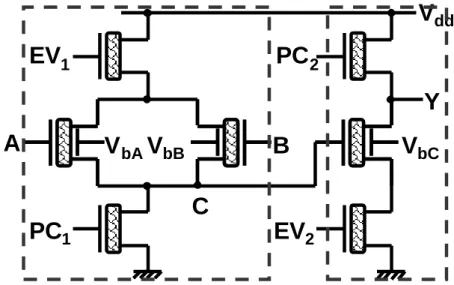
The impact of the back gate voltage polarity on the transistor channel transport characteristics opens up new opportunities for using CNTFETs in logic circuits. We have built a reconfigurable logic block which can be configured to any one of fourteen basic binary operation modes. This functionality is impossible to achieve in CMOS technology without resorting to far more co mp le x c ircu itry (and therefore silicon real estate and system power) than the cell structure described here. The polarity (n-type or p-type) of each transistor is controlled by the back-gate bias voltage values. The dynamically reconfigurable logic ce ll (DRLC_7T) is shown in fig. 3; while tab. 1 describes the 3-input configuration, corresponding basic binary logic functions and power figures for operation at 4GHz and 250M Hz e xtracted fro m transient simulations using a Ve rilog-A model adapted from [3] and parasitic capacitances extracted fro m layout estimations.
V
bA
A
V
bB
B
EV
1
PC
1
EV
2
PC
2
V
bC
V
dd
Y
C
Fig. 3. Dyna mica lly reconfigurable logic cell (DRLC_ 7T) transistor-level
schematic VbA VbB VbC Y Ptot@4GHz (nW) Ptot@250MHz (nW) +V +V +V A↓B 1.87 1.076 +V +V -V A∨B 1.85 0.99 +V 0 +V ¬A 1.83 0.84 +V 0 -V A 1.81 0.82 -V -V +V A∧B 1.84 0.9 -V -V -V A↑B 1.82 0.814 +V -V +V B/A 1.86 1.05
+V -V -V B→A 1.84 0.96 0 +V +V ¬B 1.82 0.8 0 +V -V B 1.79 0.79 0 0 0 1 1.12 0.04 0 0 -V 0 1.82 0.2 -V +V +V A/B 1.84 1.03 -V +V -V A→B 1.82 0.95
Table 1. 3-input configurations for reconfigurable cell with 3 logic levels (+ V, 0, -V) and
corresponding 14 basic binary logic functions
DRLC_7T is made up of 7 CNTFETs arranged in two logic stages: the first stage performs an ele mentary logical operation and the second stage works either in follower or inverter mode.
• A and B are boolean data inputs (voltages at A and B vary between 0V and 1V); • VbA, VbB, VbC are control inputs which configure the circu it according to tab. 1
(control bias voltages may take one of three values at -1V, 0V and 1V);
• PC1, PC2 (pre-charge) and EV1, EV2 (evaluation) are four non-overlapping clocking inputs with pre-charge and evaluation periods as in classical CM OS dynamic logic gates;
• Y is the circuit output.
We can see that Vc is evaluated between EV1 (evaluation of the first logical stage) and the next PC1 (p re-charge of the first logical stage) according to the value of inputs A and B; and Y is evaluated and ma intained between EV2 (evaluation of the second logical stage) and the next PC2 (pre-charge of the second logical stage). This clocking scheme is illustrated in fig. 4.
EV
2PC
2EV
1PC
1t
C
Y
f(A,B,V
bA,V
bB)
f(C,V
bC)
EV
2PC
2EV
1PC
1t
C
Y
f(A,B,V
bA,V
bB)
f(C,V
bC)
Fig. 4. Two-stage dynamic logic clock signal scheme
An exa mp le illustrates how this logic gate works. When VbA=VbB=VbC=1V, CNTFETs Tc1, Tc2 and Tc3 (shown in fig. 3) are a ll configured as n-type FETs, as indicated in the previous section. When PC1 is enabled, the first stage is pre-charged, and the voltage of the internal node C (Vc) is discharged to 0V. If for e xa mp le e ither of the data inputs A or B=logic "1", then when EV1 is enabled, the first layer evaluates its output such that the internal node C is set to logic "1". Then PC2 is enabled (pre-charge of the second stage), and the output Y is charged to logic " 1"; and when EV2 is enabled, the output is evaluated and Y is evaluated to logic "0". In fact in this configuration, the only situation where C is not set to logic "1" and Y therefore evaluates to logic "1" (since Tc3 is off) is when both A and B=logic "0". Th is shows that for VbA=VbB=VbC=1V, DRLC_7T is configured as a NOR operator, as specified in tab. 1. Simulat ion results of DRLC_7T in this configuration are shown in the le ft half of fig. 5 (up to 8ns) at 500M Hz operation. A fter this point, VbA,VbB and VbC change to -1V, such that CNTFETs Tc1, Tc2 and Tc3 are all configured as p-type FETs. When PC1 is enabled, the first stage is pre-charged, and the voltage of the internal node C (Vc) is discharged to 0V. If for e xa mp le either of the data inputs A or B=logic "0", then when EV1 is enabled, the first layer eva luates its output such that the internal node C is set to logic "1". Then PC2 is enabled (pre-charge of the second stage), and the output Y is charged to logic "1"; and when EV2 is enabled, the output is evaluated and Y is evaluated at logic "1". The only situation here where C is not set to logic "1" and Y therefore evaluates to logic "0" (since Tc3 is on) is when both A and B=logic "1". This shows that for VbA=VbB=VbC=-1V, DRLC_ 7T is configured as a NAND operator. VbA VbB VbC 0 0 VA VB Y 8n 2n 4n 6n 1 0 0 1 1 1 t (ns) 1 0 1 0 1 -1 1 -1 1 -1 1 0 0 0 1 0 0 1 1 1 0 0 0 1 0 1 1 1 NOR NAND 14n 10n 12n 16n 0n
Fig. 5. Simulat ion results of dynamic reconfiguration of reconfigurable ce ll
It is thus clear that this gate can realize several functions and can be dynamica lly reconfigured during the calculation.
Tab. 1 a lso gives the power consumption when DRLC_ 7T (working with 2-logic-stage control bias voltage) operates at 250M Hz and 4GHz.
It should be noted that as this is prospective work, no technology as yet exists to build this circu it, a lthough a single DG-CNTFET has been fabricated and characterized [7]. Further, significant technological advances have been made recently to achieve 95-98% horizontally a ligned semiconducting CNTs [9] and, separately, hybrid integration with CMOS [10]. Th is enables us to envisage systems using "substrates" of many aligned semiconducting CNTs with conventional meta llization and lithography techniques creating interconnections. In terms of device design, much work has focused on imp roving drive current (and therefore ma ximu m frequency and insensitivity to noise) and reliability by using an array of parallel single-wa lled ca rbon nanotubes as multip le channels in a single t ransistor with good directional and spatial control [11]. This device can pass currents of up to 1.5mA and has achieved a record current gain cutoff frequency of 8GHz. These performances are still do minated by parasitics but recent advances project that this device should reach a current gain cutoff frequency of 31GHz. Double-gate transistors using the same principle for the channel should not pose any technological obstacle.
Here we have given only one exa mple of the family of dynamically reconfigurable logic ce lls. By changing the number of the transistors we have developed 3 other logic cells wh ich can rea lize d ifferent logic function sets [3].
Clusters of cell-matrices architecture
Such fine-grain reconfigurable gates open the way towards structures which can be configured dynamica lly, for on-the-fly and partial system reprogra mmab ility. In this section, the way elementary building blocks are connected and programmed is e xplored to achieve inc reased effic iency at the application level.
Fi xe d intra-matrix interc onnec t topol ogy str ategy
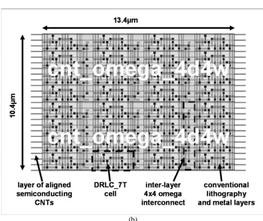
In a conventional architecture, each calculation cell wou ld be connected to the switch box d irectly. However, in the case of fine-grain logic ce lls, this approach would lead to a loss of effic iency due to a large overhead in terms of device comple xity. In the case of DRLC_7T, 7 transistors are used in the cell, wh ile a similar number of transistors (at least 6) are used for a 1-bit switchbox. In order to avoid this overhead problem, we p ropose a cluster-based approach as shown in fig. 6, wh ich consists of assembling cells in a matrix pattern, with the use of fixed intra-matrix interconnect between layers of cells. Here, the identifier fxy corresponds to the configured function of the cell and the {x,y} coordinates of the cell within the matrix. Inputs A and B are shown, as is the output Y (duplicated); precharge and evaluation connections are not shown to avoid making the figure overly cumbersome. Considering the whole of this cluster set as a new coarse grain ele ment, switchboxes
could be used for inter-matrix interconnect. It is interesting to note that matrix architectures are also particularly we ll-suited to CNTFET-based logic cells, since it is possible for single nanotubes to span several cells in the same colu mn.
L0-L1 connections f00 f01 f02 f03 f10 f11 f12 f13 L1-L2 connections L2-L3 connections f20 f21 f22 f23 f30 f31 f32 f33 f02 L0-L1 co L1-L2 co L2-L3 co L0-L1 connections L0-L1 co nections nections nections nections f03 f12 f13 f22 f23 f32 f33 f02 f03 f00 f01 f02 f03 f00 f01 f20 f21 f30 f31 f00 f01 f10 f11 f32 f33 f30 f31 f32 f33 f30 f31 L2-L3 connections L2-L3 co nections L0-L1 connections f00 f01 f02 f03 f10 f11 f12 f13 L1-L2 connections L2-L3 connections f20 f21 f22 f23 f30 f31 f32 f33 L0-L1 connections f00 f00 ff0101 ff0202 ff0303 f10 f10 ff1111 ff1212 ff1313 L1-L2 connections L2-L3 connections f20 f20 ff2121 ff2222 ff2323 f30 f30 ff3131 ff3232 ff3333 f02 f02 L0-L1 co L1-L2 co L2-L3 co L0-L1 connections L0-L1 co nections nections nections nections f03 f03 f12 f12 ff1313 f22 f22 ff2323 f32 f32 ff3333 f02 f02 ff0303 ff0000 ff0101 ff0202 ff0303 ff0000 ff0101 f20 f20 ff2121 f30 f30 ff3131 f00 f00 ff0101 f10 f10 ff1111 f32 f32 ff3333 ff3030 ff3131 ff3232 ff3333 ff3030 ff3131 L2-L3 connections L2-L3 co nections (a)
(b)
Fig. 6. Tile-based approach for the integration of regularly structured matrices of
reconfigurable cells (a) conceptual schematic (b) layout for two tiles of 4d4w M odified-Omega topologies
For intra-matrix interconnect, and taking wiring co mple xity into account, we eliminate any total interconnectivity topologies at the outset. Instead, and through analogy to computer networks, we adapt inco mplete interconnection sets to the matrix architecture. In fact, Multistage Interconnection Networks (MIN) are designed to interconnect layers in an efficient way and can be applied in this context.
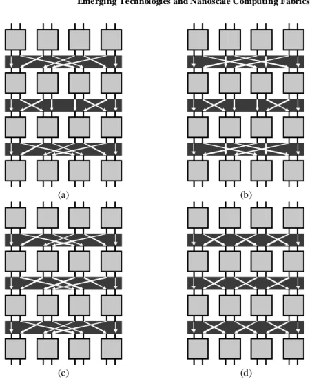
Of course, there are many topologies or combinations, but we focus principally on 4 typical permutations [12]: Banyan (fig. 7(a)), Baseline (fig. 7(b)), Flip (fig. 7(c)) and Modified-Omega (fig. 7(d )), where the modifications to standard Omega ma ximize the shuffling in this topology. In co mputer science, MINs are used to interconnect layers of switchboxes in order to route information packets only. In this application, the main diffe rence is that switchboxes have been removed and replaced by logic cells, introducing computing directly inside the network.
(a) (b)
(c) (d)
Fig. 7. M atrix of 16 reconfigurable gates with various interconnect topologies: (a) Banyan (b)
Baseline (c) Flip (d) M odified-Omega
Matrix progr amming
It is useful to combine such novel types of nanodevice-based reconfigurable cell with the e xplorat ion of new function mapping methods in anticipation of the deployment of incomplete-operator cluster-based systems. A primary objective is to analyze the limits of such architectures when mapping a co mp le x software application onto it. Many parameters must be considered to program the nanodevice-based architectures:
• the number of ce lls in matrix
• the topology of cells interconnections • potentially, the faults present in the matrix
Moreover, several metrics have to be optimized (co mputation speed, area, etc). Therefore, new CAD tools meeting these requirements are mandatory in order to e xplore the potential of nanodevicebased architectures during the prototyping phase. One of the key issues is the automatic mapping of comp le x functions onto nanodevice-based architectures. Several mapping methods defined for conventional architectures have been proposed. However, these methods fail to reach the ultra-fine granularity specific to nanodevice-based architectures. Furthermore, they do not consider connectivity restrictions and dynamic reconfiguration opportunities.
While the application is quite close to logic synthesis and network routing, the fact that we have introduced computing inside the matrix means that we cannot use routing algorithms or synthesis algorithms directly. We present in this section a mapping method designed to map a logic function graph onto the architecture described above. First, we will describe the method, and then we will give an e xa mple to show how this method works.
Functi onal description
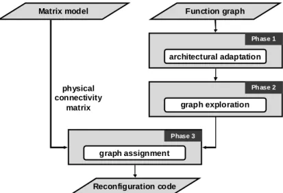
The described method inputs the function graph to map and the physical connectivity matrix and outputs the map of logic e le ments onto physical cells. The algorith ms work using adjacency matrices. In such matrices, (i,j) re fers to the intersection of the row i and colu mn j. A 1 at the position (i,j) means that the point i is connected to the point j. These matrices are essential to subsequent processing steps, described in fig. 8.
Matrix model Function graph
architectural adaptation Reconfiguration code Ph ase 1 Ph ase 2 physical connectivity
matrix graph exploration
Phase 3 graph assignment
Fig. 8. M apping method functional stream
Phase 1: Pre-processing of function graph
In a first operation, we have to adapt the logic function to our architecture. Due to the layered structure, the system is pipe lined. Function graphs have to be processed by
adding necessary synchronization ele ments (to extend input and output paths of data), as well as removing jumps over logic layers (to conform to the physical topology). To identify logic layers in function graphs, we d ivide the associated adjacency matrix into small matrices Cnm. Cnm is the adjacency matrix between the points in the logic layer n and those in the logic layer m. We therefore pay particular attention to matrices where m ≠ n+1 because the presence of any non-zero ele ment in these three matrices identifies a connection which “ju mps” at least one logic layer. Such a direct connection cannot be realized in the topology since the interconnect topology is physically fixed. The solution is to add synchronization ele ments (i.e. create a path instead of a jump), then repeat the process until no more connections jump logic layers.
Phase 2: Recursive exploration
The processed function graph is then analyzed in depth, mean ing that for each node in the structure, child branches are identified and recursively e xp lored.
Phase 3: Node assignment
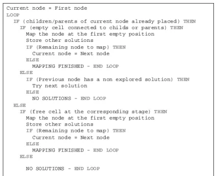
Logic nodes are then assigned to cells. This is done according to the physical interconnections. Each layer's connections are compared to the relevant inter-layer connectivity matrix – allowing (or not) the assignment of functions to cells. Branching (i.e. the e xp loration of the immediate ly preceding a lternative) is used when the arbitrary choice leads to a dead-end, and the process is repeated until all functions are assigned to cells. The algorith m of th is step is shown in fig. 9.
Current node = First node LOOP
IF (children/parents of current node already placed) THEN IF (empty cell connected to childs or parents) THEN
Map the node at the first empty position Store other solutions
IF (Remaining node to map) THEN Current node = Next node ELSE
MAPPING FINISHED - END LOOP ELSE
IF (Previous node has a non explored solution) THEN Try next solution
ELSE
NO SOLUTIONS - END LOOP ELSE
IF (free cell at the corresponding stage) THEN Map the node at the first empty position Store other solutions
IF (Remaining node to map) THEN Current node = Next node ELSE
MAPPING FINISHED - END LOOP ELSE
NO SOLUTIONS - END LOOP
The algorithm has been imp le mented in Matlab, and executes in under 0.1s for a complete 16-node mapping operation using a standard 2GHz PC. While this approach enables the mapping of simple functions to the fixed-interconnect matrix based on the reconfigurable ce lls, function partition ing and merg ing methods will be required to map mo re co mple x functions over several matrices.
Mapping e xample
As an exa mp le, we consider a matrix which is 4 cells deep and 4 cells wide (4d4w) using a Banyan interconnect topology (fig. 7(a)). Individual cross-connectivity matrices Xnm (X01, X12 and X23) between logic cell stages of depth n to m are shown in eq. 1.
=
=
=
1
0
1
0
0
1
0
1
1
0
1
0
0
1
0
1
,
1
1
0
0
1
1
0
0
0
0
1
1
0
0
1
1
,
1
0
1
0
0
1
0
1
1
0
1
0
0
1
0
1
23 12 01X
X
X
(1)The function to map is represented by a graph, generated by a random graph generator for test purposes. During the graph adaptation step, we pay particular attention to the matrices C02, C03 and C13 containing 1's. As mentioned previously, such matrices represent connections which “jump” at least one logic layer, and are impossible to realize. In this e xa mple , the connections between points (2, 6), (5, 8) and (4, 9) are the three connections to be adjusted.
The graph exp loration is then launched and we obtain the following sequence (p* represents synchronization nodes):
p1-p4-p*-p9-p5-p7-p3-p*-p*-p*-p8-p2-p*-p6-p*
Finally, the graph assignment is performed. In the e xa mp le, the first point p1 is assigned to the cell f00. According to the path defined in the previous step, p4 is the next point to assign to a cell in the matrix. Since f00 is physically connected to f10 and f12, the cell with lowe r y-inde x (he re f10) is arb itrarily chosen for p4 assignment, and the other possibility is me morized. In our e xa mp le, the fina l progra mmed matrix is shown in fig. 10. In this figure, we can see the nodes of the logic function graph and the nodes added for synchronization purposes (circ les with no names) correct ly placed on the cell matrix.
p1 p1 pp22 ff0202 p*p* p4 p4 p*p* pp55 pp33 p* p* pp66 pp77 p*p* p9 p9 p*p* p*p* pp88
Fig. 10. M atrix after function mapping
Evaluati on methodol ogy
The aim of this part of our work was to evaluate and compare performance metrics for the 4 interconnect topologies. Our study was made on a 4d4w matrix using the previously mentioned intra-matrix interconnection topologies. 4d4w matrices have been chosen because of a good balance between comple xity and simulat ion time. We evaluated various metrics: the success rate of mapping function graphs, the fault tolerance and the average interconnection length. We have carried out detailed analyses to compare the efficiency of the different intra-matrix interconnect topologies. We use a random graph generator to generate static sets of function graphs containing 6-16 points, in order to have fixed comparison criteria between topologies. No graphs contain isolated nodes, as here we focus on fixed interconnect layers, which are severely penalized by isolated nodes. We consider therefore these cases to be an overload issue to be solved by specific architectural customizat ion. Each set, corresponding to a given number of points in the function graph, contains 1000 samples. Using the previously described mapping method, each function is programmed onto the 4d4w matrix using the various intramatrix interconnect topologies, ideal or faulty, and metrics are calculated. Fig. 11 summa rizes the evaluation methodology and the associated parameters.
Mapping
method
0-fault connectivity matrix connectivity matrix fault distribution parameters function graph … omega flip banyan baseline … omega flip banyan baseline topology dimensions d,w manual definition success rates configuration codes random generation real connectivity matrixFig. 11. Evaluation method
0% 10% 20% 30% 40% 50% 60% 70% 80% 90% 100% 6 7 8 9 10 11 12 13 14 15 16
% cas exploitable Oméga - 0 défaillanc e Banyan - 0 défaillanc e Baseline - 0 défaillance F lip - 0 défaillance
omega topology can achieve up to 25% more functions % exploitable cases 0-fault baseline 0-fault omega 0-fault flip 0-fault banyan 40%@12pt 20%-30%@12pt 90%@6pt 75%-80%@6pt
Fig. 12. Programmability success rates for Banyan, Omega, Flip and Baseline interconnect
topologies within 4d4w matrices
Applying static sets to ideal interconnect topologies, we can test the ability of the matrix-topology ensemble to have co mple x functions mapped onto it. Considering the percentage of function graphs successfully mapped onto matrix with respect to the number of samp les in the set, we obtained the success rate. Fig. 12 shows the comparison of success rates for 4d4w Banyan, Omega, Flip and Baseline topologies. For Banyan, Flip and Baseline interconnect topologies, the success rate is about 80% when the function graphs have 6 points. At 12 points, the success rate is about 25%. The difference between these two topologies is thus relatively small. However for the
Omega interconnect topology, the success rate is about 90% for 6-point function graphs and about 40% for 12-point graphs. This clearly shows that the Omega interconnect topology is more suitable for this type of mat rix.
This is because this topology is has less symmetric redundancy than the other topologies and spreads calculations over cells occupying less width, which seems to correspond better to typical function graphs. In fact in the matrix, there are pairs of cells which have the same inputs. For two cells which have the same inputs, the sum of the number of functions they can achieve is 14. For t wo cells which do not have the same inputs, the sum of the number of functions they can imp le ment is 14+14 = 28. In the Banyan topology for exa mple, there are 6 pairs of cells which have the same inputs, while in the Omega topology, there are only 2. This is the ma in reason why the Omega topology has the potential to realize more functions than other topologies.
It is worth noticing that the use of a MIN reduces the number of mapped logic functions, compared to traditional LUT approaches. Such a proble m is managed at a higher hierarchica l level. For e xa mple , if a function graph cannot be mapped onto a single matrix, we can split it and map the subgraphs onto different matrices.
Cluster pr ogramming
At the cluster level, an e xtra layer of para mete rs and additional fle xib ility is introduced. It is possible to consider clusters of varying matrix size, as well as the e xecution of functions in paralle l, and the dynamic (potentially cycle-level) reconfiguration of each matrix to achieve highly optimized graph e xecution. In order to exp lore these aspects, a cluster-level mapping model is proposed. This mapping model places applications onto the complete architecture co mposed of several matrices, such that multip le metrics are optimized. These metrics are :
• communicat ion cost • configuration cost • e xecution time
• number of unused logical ce lls.
The objective of the mapping model is to optimize the place ment of a co mp le x function onto the architecture. It considers the structure of the architecture, the scalability require ment as we ll as the dynamic reconfigurat ion imp lying a h igh-level of pipelining and parallelis m. It co mbines GA and partitioning approaches.
Model Description
The proposed model is shown in fig. 13. It takes as inputs a function graph and the architecture model and generates the reconfigurable code of the mapping as output. In general, co mple x functions cannot be mapped onto a single matrix. For this purpose, functions are partitioned into sub-functions. Thus, in order to map a comple x function onto a cluster of matrices, two mapping levels are perfo rmed:
• Firstly, each sub-function is mapped onto a matrix using the method described in the previous section;
• Then, the dependency graph of sub-functions is also mapped onto the cluster of matrices.
Architecture model Application graph partitioning matrix mapping Reconfiguration code Phase 1 Phase 2 global mapping matrix information cluster information
Fig. 13. M apping model
The function to map is represented as a Direct Acyclic Graph (DA G) Gf = (Ef, Vf) where Vf is a set of nodes representing logic operations, and Ef a set of direct edges dependency relations between nodes.
Phase 1: Partitioning and matrix mapping
The aim of the first step is to partition a function graph into smaller sub-graphs so that each sub-graph fits in a single matrix. For this purpose, partitioning and matrix mapping methods are processed. To be valid, a partit ioning result must respect the following constraints:
• The total number of operation in the sub-graphs is the same as the one in the initial graph
• There is no cyclic dependency.
Each sub-graph obtained during partitioning is mapped onto the matrix using the matrix mapping method defined previously. An exhaustive research is performed to ensure that the best mapping is found. If the matrix mapping fails, the partitioning is modified and new matrix mappings are performed. This exp loration loop, represented in fig. 13 through a feedback arrow, is performed until the sub-graphs fit in a single matrix. The result of the first step is a new graph composed of subgraphs and a set of mapping solutions associated to each subgraph.
Phase 2: Global mapping
The second phase maps the set of sub-graphs obtained during the phase 1 onto the cluster of matrices. The objective is to find a mapping and an execution order minimizing the commun ication cost, the configuration cost, the number of ce lls
non-used and the execution time. A Fast Elit ist Non-Do minated Sorting Genetic Algorith m (NSGA II) [13] is used to minimize these metrics.
A mapping solution is encoded as a two part chromosome (fig. 14): the first part represents the execution order of the subgraphs; the second part gives the matrix on which sub-graph are executed. For exa mple , in fig. 14, the set composed of subgraphs Sb0, Sb1, Sb2, Sb 3 and Sb 4 is e xecuted on matrices Gm1 and Gm2. Thus, Sb 1 and Sb4 are e xecuted in parallel on matrix Gm1 respectively Gm2 at cycle 0. The e xecution of sub-graphs Sb0, Sb 2 and Sb 3 is pipelined on Gm2. For this purpose, Gm2 is dynamica lly reconfigured two t imes.
4
0
5
6
0
Gm2 Gm1 Gm2
Gm2
Gm2
order of execution
matrix for mapping
Fig. 14. Global mapping solution encoding
Experi mental results
To evaluate the efficiency of the proposed approach, we used Xilin x-Virte x-4 [14] schematic designs. Each circuit is characterized by the number of operations, the number of dependencies and the depth (i.e. the length of the longest path in the circuit ). The designs are modified to reach the granularity required for the logic ce ll (two 1-b it inputs and two 1-bit outputs). The target architecture is based on Modified-Omega c lusters of 4d4w matrices. The e xpe rimental results are given in tab. 2, in terms of the nu mber of sub-functions obtained after the partitioning phase, the number of dependencies between sub-functions, the ratio between the number of logic operations and the number of sub-functions (fill factor) and finally the number of failures for matrix mapping during partitioning.
These results depend on the following factors:
• the size of the circuit: In the partitioning, no cyclic dependency is allowed between sub-functions. Moreover, the restriction of connectivity must be respected in order to route data coherently in matrices. So, part itioning results depend on number of dependences and the size of the circuit.
• failures on matrix mapping: During partitioning when a sub-graph cannot be mapped onto a matrix, the sub-graph has to be partitioned until it can be mapped. This case occurred twice fo r CMP8, i.e. the corresponding graph was reduced three times. Benchmk circuit No. operations No. dependencies Logical depth No. sub-functions No. dependencies Fill factor (%) No. hw placement failures ALU2 45 64 14 6 9 46.9 1 CMP8 59 75 11 9 14 40.6 2 ADD8 101 132 22 11 18 57.4 0 ADSU8 133 180 25 18 30 45.8 0 CMP16 142 189 22 19 41 46.7 2 ADD16 197 260 38 21 36 58.6 0
ADSU16 261 356 41 27 49 60.5 1
Table 2. Experimental cluster mapping results for Xilinx-Virtex-4 benchmark functions
Insights and future challenges
In this work, we have firstly e xp lored some of the opportunities opened up by the electrica l behaviour of the double-gate CNTFET. We focused primarily on a specific property, namely the enabling of p-type or n-type device behaviour to be achieved in the same CNTFET according to the voltage applied to the back-gate. We have developed a family of dynamica lly reconfigurable logic cell, based on these devices and configured by the set of back gate bias voltages. These fine-grain reconfigurable cells have been considered as a universal reconfigurable cell enabling the synthesis of any Boolean function.
We then introduced a cluster-based matrix a rchitecture useful for fine-gra in reconfigurable logic cells based on emerg ing devices. This cluster-based architecture uses fixed interconnection topologies in order to reduce the overhead induced by conventional approaches. We have proposed a method to map specific functions to the matrices of reconfigurable ce lls. This method has been used to analyze intra-matrix topologies with respect to various metrics and shown that the mapping success rate is about 90% for 6-point function graphs and about 40% for 12-point graphs when using the Modified-Omega interconnect topology in a 4x4 matrix. This new function mapping method is a key step towards using fine-gra in reconfigurab le cells for the on-the fly and partia l reprogra mmability.
Finally, we proposed a methodology for mapping applications onto the cluster-based architectures. This model enables the exploration of the potential of this type of architectures for future applications and was used successfully to map comp le x benchmark functions onto the architecture. The model consists of two main steps accomplished through three comple mentary methods: partitioning, matrix mapping and cluster mapping.
The e xperience ga ined through this work lead us to believe that carbon-based computing fabrics can be a suitable support for pervasively deployment in many industries such as communications, energy, transport and healthcare. Tomorro w's computing platforms must achieve high computing throughput at very low power, while maintain ing a level of robustness and capacity to be redeployed to new applications via software programming on very flexible hardwa re. In this way, engineers and scientists can benefit fro m almost unlimited co mputing power and can concentrate on developing imaginative and high added-value applicat ions, while seamlessly supported by highly fle xible and automatically configurable hardware and software programming mode ls.
Such design of nanofabrics is at the interface between two scientific co mmunities: that of nanoscience and nanotechnology on one hand, and that of data processing and embedded systems on the other. Critica l challenges from the design point of view are to be able to understand how such devices can best be used in architectures and indeed if they can be expected to deliver significant benefits at this level, and to
e xtend existing design and simulat ion approaches to take into account the nanoelectronic approach. Close collaboration between designers and technologists is key to the strengthening of mutual design approaches necessary for the development of nanoelectronic systems and the generation of truly original designs explo iting the specific properties of nanodevices. The outcome of such collaboration is a clearer understanding of choices among the broad spectrum of potential devices and possible technologies capable of challenging conventional approaches in future nanoscale applications.
In our view, technology is evolving at such a rate that it is necessary to break the traditional technology – device – compact model – circuit – architecture development cycle by focusing on the fast-track integration of new devices into many-core computing platforms, through the imple mentation of a vert ical and integrated research approach. In this way, circuit and architectural design activities are based on reasonable hypotheses issuing from device and technology work, and the development of the afore mentioned devices and technology is focused towards the needs of high-level architectures.
References
1 TOP500 Supercomputing Sites, 2009. Available at http://www.top500.org
2 International Technology Roadmap for Semiconduc tors, 2007 edition. Available at http://public.itrs.net
3 O'Connor, I. et al. (2007), 'CNTFET Modeling and Reconfigurable Logic-Circuit design', IEEE Trans. Circuits and Systems, Vol. 54, No. 11, pp.2365-2379
4 Chau, R. et al., (2005) ‘Benchmarking Nanotechnology for High-Performance and Low-Power Logic Transistor Applications’, IEEE Trans. Nanotechnology, Vol. 4, No. 2. 153. 5 Raychowdhury, A., Roy, K., (2005) ‘Carbon-Nanotube-Based Voltage-M ode M
ultiple-Valued Logic Design’, IEEE Trans. Nanotechnology, Vol. 4, No. 2, pp. 168-179.
6 Sordan, R., Balasubramanian, K., Burghard, M ., Kern, K., (2006) ‘Exclusive-OR gate with a single carbon nanotube’, Appl. Phys. Lett., Vol. 88, 053119.
7 Lin, Y., Appenzeller, J., Knoch, J., Avouris, P., (2005) ‘High-Performance Carbon Nanotube Field-Effect Transistor With Tunable Polarities’, IEEE Trans. Nanotechnology, Vol. 4, No. 5, September 2005
8 M oritz, C.A. et al., (2007) "Fault-Tolerant Nanoscale Processors on Semiconductor Nanowire Grids", IEEE Trans. CAS I, vol. 54, no. 11, p. 2422
9 Ding, L., Tselev, A., Wang J., et al., (2009) ‘Selective Growth of Well-Aligned Semiconducting Single-Walled Carbon Nanotubes’, Nano Lett., Vol. 9, No. 2, p. 800. 10 Akinwande, D., Yasuda, S., Paul, B., Fujita, S., Close, G., Wong, H.S.P., (2008)
‘M onolithic integration of CMOS VLSI and carbon nanotubes for hybrid nanotechnology applications’, IEEE Trans. Nanotechnology, Vol. 7, No. 5, p. 636.
11 Beyhoux, J.-M ., Happy, H., Dambrine, G., Derycke, V., Goffman, M ., Bourgoin, J.-P., (2006) ‘An 8-GHz ft Carbon Nanotube Field-effect transistor for Gigahertz Range Applications’, IEEE Electron Device Letters, Vol. 27, No. 8, pp. 681-683.
12 Adams, G.B., Agrawal, D.P., Siegel, H.J., "A Survey and Comparison of Fault-Tolerant M ultistage Interconnection Networks," Computer, vol. 20, no. 6, pp. 14-27, June 1987. 13 Kalyanmoy, D., "A Fast Elitist Non-Dominated Sorting Genetic Algorithm for M
ulti-Objective Optimization: NSGA-II", IEEE Trans. Evol. Comput., vol. 6, no. 3, p. 149, 2002 14 Xilinx, "Virtex-4 Libraries Guide for Schematic Designs," 2009
![Fig. 1. Best observed processing performance for a single machine [1] (a) and predictions for processing performance in a single chip [2] (b)](https://thumb-eu.123doks.com/thumbv2/123doknet/13389449.405291/3.892.204.694.235.491/observed-processing-performance-single-machine-predictions-processing-performance.webp)
![Fig. 2. Double-Gate CNTFET structure [7] (a) top view (b) cross-sectional view](https://thumb-eu.123doks.com/thumbv2/123doknet/13389449.405291/5.892.275.635.458.828/fig-double-gate-cntfet-structure-view-cross-sectional.webp)