A 250 W High Density Point-of-Load
Converter
by
Andrew Ferencz
S.B.E.E., Massachusetts
Institute
of Technology
(1987)
Submitted in Partial Fulfillment
of the Requirements for the
Degree of
Master of Science
in Electrical Engineering and Computer Science
at the
Massachusetts
Institute of Technology
September, 1989
@
Massachusetts
Institute of Technology, 1989
Signature of Author - .. -- -v ' ...- ..
-Department of Electrica/Engine~ d Computer Science
Septemb"er, 1989
Certified by .
) __~ __ ~ssor ~rtin F Schlecht
~~~ ~ Th~pervisor
Accepted b~ __-__ ' ...-___.-
._-=_~-~~--- ...
...---Professor Arthur C. Smith
Chairman, Departmental Committee on Graduate Students
A 250 W High Density Point-of-Load Converter
by
Andrew Ferencz
Submitted to the
Department of Electrical Engineering and Computer Science
on September 1, 1989 in partial fulfillment of the requirements
for the Degree of Master of Science.
Abstract
This thesis describes the design and construction of a 250 W, 35-60 Vin,
5 V
out dc-dc power converter with a switching frequency of 500 kHz. Theconverter uses square wave switching and is composed of two power
process-ing stages in series. The first stage, a boost converter, regulates the output
voltage of the converter. The second stage, a push-pull converter operating
at 100% duty-cycle, provides isolation and steps the bus voltage created by
the first stage down to the load voltage.
The converter was fabricated using a copper thick film process with
commer-cially available surface mount components. This fabrication method
mini-mizes parasitic inductances and allows the designer to reduce the coupling
of the noise generated in the power section into the control section.
The converter had an efficiency of 82% at full power and achieved an
un-packaged power density of 80 W fin3
• During a 15 A transient in the output
current, the peak error in the output voltage was 3% and the output voltage
was within 1.5% of the regulated voltage after 10 j.Ls.
Thesis Supervisor: Professor Martin F. Schlecht
Acknowledgements
I would first like to thank my thesis supervisor, Professor Martin F. Schlecht,
for his guidance and inspiration. Under his tutelage, I have come to
under-stand and learn to apply much of what I have been taught since coming to
MIT.
I wish to thank my parents for their support, both emotional and financial,
and to let them know I love them very much.
I wish to thank Peter Price of Unitech, Ron Carpenter of Qualidyne, and
John Reid of Coutant for their support and advice in this work.
I wish to thank Phil Hower of Unitrode for supplying me with parts and
offering valuable advice.
To my grandmother, brother, and sister-in-law, I could not dream of a nicer
and more loving family.
To my girlfriend, your love and support has given me the strength to pursue
my goals.
To the Moose who tried hard to subvert my acedemic career, thanks much (smiles ).
Contents
1 Introduction
1.1 High Density Power Supplies.
1.2 Achieving Higher Power Density .
1.3 High Frequency Converters .
1.4 Thesis Description .
2
Two Stage Converters
2.1 Two Stage Converter Efficiency .
2.2 Advantages of Two Stage Converters ..
2.3 Disadvantages of Two Stage Converters.
3
Power Stage Design
3.1 Specifications .
3.2 Isolation Stage (Push-Pull Converter) .
3.2.1 Operation at 100% Duty-Cycle 3.2.2 Zero-Voltage Switching . 3.2.3 Load Regulation . 3.2.4 Output Filter . 3.2.5 Circuit Diagram . 3.3 Pre-Regulator .
3.3.1 Designing the Pre-Regulator .
3.3.2 Paralleling Converters .
3.4 Design Summary .
4 Design and Implementation of Control Circuitry
4.1 Control of the Boost Converter ...
4.1.1 DCM Boost Converter Dynamics .
4.1.2 Implementing the Control .
4.2 Control of the Isolation Stage .
4.2.1 Flux Balancing Dynamics .
4.2.2 Implementing the Flux Balancing Circuit .
4.3 Powering the Control Circuitry .
8 11
12
14 18 1920
28
31
32
32
33
33 34 38 4044
44
4952
53
5555
5662
63 64 67 685
Fabrication of the Power Circuit 695.1 Copper Thick Film
...
705.2 Layout Issues
...
71 5.2.1 Magnetic Coupling . 71 5.2.2 Capacitive Coupling 81 5.3 Magnetics Design ... 86 5.3.1 Transformer Design .. 86 5.3.2 Inductor Design . 89 5.4 Output Rectifiers ...
90 5.5 Assembly ... ... , 92 6 Experimental Results 94 6.1 Push-Pull Stage ... 95 6.1.1 Testing .... 95 6.1.2 Waveforms. 96 6.2 Boost Converter .. . . 100 6.2.1 Testing ... . 100 6.2.2 Waveforms. ... 100 6.3 Efficiency....
. 103 6.4 Load Regulation . 1047
Conclusions105
A
Data sheets107
List of Figures
1.1 A point of load power system, [1] , Fig. 1.4 9
1.2 Core loss data for Ferroxcube 3F3 material. 16
1.3 Proximity effect due to thick copper immersed in AC
jj
field. 172.1 A block diagram of a two stage converter 20
2.2 Two stage vs. single stage converter each operating at 500 kHz 22
2.3 Schematic showing energy storage on transformer's primary side 29
3.1 The isolation stage, a push-pull converter .. 34
3.2 Circuit diagram for transition analysis 35
3.3 Model of isolation stage transformer 36
3.4 Output current showning effect of L/R time constant 41
3.5 Model used to determine value of output inductor 43
3.6 Model for the output filter ... 43
3.7 Schematic diagraII?- of converter 45
3.8 Boost converter 46
3.9 Waveforms for understanding design equations .. 50
4.1 Current mode control waveforms and behavior . 57
4.2 Circuit and waveforms showing behavior of boost converter
using current-mode control 58
4.3 The loop transimission 60
4.4 Effect of ripple on the gain of system . 61
4.5 Gain of power train and control circuit 62
4.6 Model for determining flux balancing dynamic equations 65
4.7 Push-pull feedback loop 66
91
9374
75
76
77
77
795.2 A single point ground connection .
5.3 A multiple point ground connection .
5.4 Simple transformer model for flux linkage.
5.5 Effect of orientation on magnetic coupling
5.6 Laying out circuit to minimize magnetic coupling
5.7 Using copper walls to direct flux .
5.8 Construction of current sense resistor using copper thick-film
material 79
5.9 Interdigitated capacitors used to reduce lead inductance
prob-lems 81
5.10 Common-mode noise generated in a transformer 83
5.11 Methods of reducing common-mode capacitance: (a) thicker
insulation, (b) reducing voltage, (c) shielding 84
5.12 Side view of barrel wound transformer, from [2] 87
5.13 Masks used for constructing transformer windings 88
5.14 The slit cut in the copper help reduce copper lossed due to
fringing fields 89
5.15 View of secondary side showing low inductance connection and
use of unpackage diodes ...
5.16 Completed power converter
6.1 Drain-source voltages of two isolation stage MOSFETs with
no load 97
6.2 Drain-source voltages of two isolation stage MOSFETs with
125 W load 98
6.3 Turn-off transition of isolation stage, D-S vs. G-S 98
6.4 Turn-on transition of isolation stage, D-S vs. G-S 99
6.5 Waveforms showning flux-balancing, D-S vs. CbU8 99
6.6 The Output Ripple at 50 W. The magnitude of the ripple was
fairly constant over entire power range 101
6.7 Vout during transition from 10 A to 25 A 101
6.8 Vout during transition from 25 A to 10 A 102
6.9 Cbu8 during 25 A to 10 A transient showing effect of load
regulation 102
Chapter
1
Introduction
Distributing power in electrical equipment at a high voltage, and then step-ping it down to the needed voltage at the load both, both reduces the size
of the distribution bus and permits local regulation. Modules which
trans-form and regulate from one dc bus to another are used in many different
applications in the telecommunications, aerospace, and military industries.
However, in most of today's computer systems, power is bussed directly at the low load voltage (e.g. 5 V). Over the last several years the power
elec-tronics community has focussed its research on the distribution of power at
a high dc voltage (e.g. 40 V) which is then stepped down to the load
volt-age with a converter mounted on each circuit board. This method, ~alled
a distributed power supply system, will be needed even more as the logic
voltage drops from 5 V to 3.3 V since the requirements for regulation and ripple become stricter.
pc board
VBe front end 30-40 Vde
converter
pc board
pc board
density, improve the performance, and increase the understanding of high frequency switch-mode converters, describes the design and development of a 250 W, high power density converter. This point of load (P.O.L.) converter may be used in a distributed power system as shown in Fig. 1.1.
The converter is similar to the converter designed for the 10 MHz project at MIT [1] [2]. However, the focus of the 10 MHz project included component design (synchronous rectifier, integral turn-off MOSFE.~), a new topology,
copper thick film technology, novel optimized magnetic structures, and
spe-cial control and MOSFET driver IC's. The converter described in this thesis, in comparison, uses commercially available parts, although it takes advantage of some of the knowledge and developments learned in the other endeavor.
This converter incorporates technology that may not be commercially
vi-able today, both in cost and manufacturability, because it uses large
(> l/LF)
ceramic capacitors, copper thick film technology, and unpackaged Schottky rectifiers. Large ceramic capacitors are very expensive and have mostly been
used in converters for military applications. Copper thick film technology
is more difficult to work with than the established gold and silver technolo-gies because copper oxidizes readily. Finally, the reliability of unpackaged large area Schottky diodes is not known and requires further study. However, the converter does show what is possible (in efficiency, power density, and transient performance) given the components available today.
It is not fully known what will be required of point-of-Ioad converters!.
Prototype converters, such as the one described in this thesis, help define
standards and allow a preview of what may be the future of power electronics. The availability of these new converters will change the way system designers
incorporate power into their products. This change will come during and
after the power electronic designers show and perfect that which can be accomplished using new technology and better designs.
1.1
High Density Power Supplies
The need is growing for denser, lighter, and more reliable power supplies.
Power supplies have not kept pace in the drive toward miniaturization of
electronic equipment. In the aerospace and automotive industry, where
min-imizing weight improves performance and lowers manufacturing and
oper-ating costs, lighter power supplies that perform as well or better than old designs would have a considerable advantage in the market.
As converters become small enough to be considered components, it will be easier to create standards that will help reduce the practice of designing
a converter for every new application. This.might also reduce the
fragmen-tation of the power electronics industry, where today many little companies
each have a small share of the market. With standard converters, the
cus-tomer will be able to incorporate power into his system with less problems.
1For example, does the converter need isolation or not?, how does being very close to
Second sourcing will enhance competition, resulting in lower prices and
im-proved products. Standardization of converters into components may also
lead to manufacturing breakthroughs. For instance, almost all of today's
power converters have some hand assembly which increases their manufac-turing costs and can lead to reliability problems.
Standardization may take this form: front end converters designed with
power factor correction, safety isolation, and an ability to operate from ac mains anywhere in the world create a mid-range voltage (e.g. 40 V) for a
distribution bus. Standard DC-DC modules with known efficiency, thermal
requirement, noise, and reliability would then be used as P.D.L. converters. These P.G.L. modules would be available with single or multiple outputs having voltages at +5 V, :l:15 V, and with power levels of 25 W, 50 W, 100 W, and larger.
1.2
Achieving Higher Power Density
Much of a converter's volume is comprised of energy storage elements. The canonical switching cell [16], from which dc-dc converters are derived, trans-fers energy in discrete intervals. Filter elements are used on the input and output ports to smooth the power flow, i.e., take a dc current from the power
source and deliver a dc voltage to the load. Because a power converter is
ideally 100% efficient, these filters are composed of inductors and capacitors. As the switching frequency of the converter is increased, smaller values of
inductance and capacitance2 are needed for low-pass filtering, which saves
both money and volume. Therefore, the push toward high power density has mostly been a push toward higher switching frequencies.
For example, the energy in an inductor is stored in fields confined in the magnetic material and air gap. Because magnetic material saturates, both the magnetic material and the air in the gap have a maximum magnetic energy density3. Because more energy is stored in the air gap than in the magnetic material, the inductor's maximum energy storage can be increased by increasing only the size of the air gap. If the air gap is doubled, to first order the value of inductance will decrease by two and twice the dc current can flow before saturation of the magnetic material occurs, i.e., the energy storage has increased by a factor of two. Because the maximum current has
increased by two, however, the ]2R loss has increased by four. Thus, for the
same size magnetic element, the magnetic energy storage can be increased
if an increase in power dissipation can be tolerated. Otherwise, a larger
magnetic element is needed4
• A switching converter operating at a higher
frequency needs less magnetic energy storage, and therefore a smaller size inductor.
The transformer in a converter can also be made smaller by increasing
2The capacitor's dc voltage and the inductor's dc current remain the same because the
power level has not changed.
3For a complete discussion on transformer and inductor design, see [12]. For a discussion on optimizing a transformer's size, efficiency, and structure, see [7].
4An inductor's Q,wL/ R, has the physical dimensions of (length)2, i.e. a larger inductor has a bigger Q.
the switching frequency. The magnetic material of the transformer is limited
by saturation. The flux swing in a transformer is calculated from
fj.B
=(V)(T)
AeN
where V is the applied voltage,
Ae
is the area through which the flux passes,and N is the number of turns. Given a maximum ..6.B,in order to decrease
Ae,
i.e., use a smaller transformer, either N must be increased or T mustbe decreased. Because a core with a given
Ae
has a fixed winding area forcopper, doubling N (because
Ae
was halved) increases the resistance of thewinding by a factor of four which reduces the transformer's efficiency. By
decreasing T (increasing the switching frequency; in this case doubling the frequency), a smaller core can be used with the same valu'e of ..6.B,N, and V.
1.3
High Frequency Converters
Most square-wave switching converters loose the energy stored in the
par-asitic inductances and capacitances during each switch transitions. Also,
because the switches are turned on with an inductive load, during commuta-tion the switch carries current and supports voltage at the same time, causing energy to be dissipated [1, p. 43]. Because switching losses are energy lost per cycle, the power loss from switching losses increases linearly vvith
fre-quency. Therefore, the switching.frequency is limited by the desire to make
In order to raise the switching frequency, designers have been using res-onant and quasi-resres-onant topologies [9] [10] [11], which eliminate or reduce the switching losses. Without switching losses, the switching frequency can be increased until the resonant elements, which may be the parasitic
induc-tances and capaciinduc-tances, cannot be made any smaller. However, resonant
converters have larger device stresses; peak voltages and rms currents; than
square wave converters. Thus, resonant converters have more conduction
losses than square wave ones for the same area FET or rectifier.
Very high
(>
5 MHz) frequency operation has other limits. For example,magnetic materials are more lossy at higher frequencies, especially at appre-ciable flux densities. As seen in Fig. 1.2, losses increase faster than linearly with frequency. This places an upper bound on the frequency at which mag-netic material can efficiently transmit power or store energy. Because ferrite
is a very poor conductor of heat5
, the core loss may have to be less than one
could tolerate for converter efficiency reasons alone. Consequently, raising
the switching frequency may not lead to smaller inductors and transformers because the ac flux needs to be reduced. In fact, many of the new high fre-quency designs only use 1/10 or less of the flux swing that core saturation would allow [13] [15].
As the frequency increases, the skin effect limits the amount of copper
that carries the ac current. This may increase the power loss vvhich cannot
I~
R6ro.SSfV~
:Jt:''.
IJD
iOO°C
I (=- .1 I I !JI I I / .:/~I1)
-I -~~Z,~l
\~
ftA~/ /
/
II~J'V(/
I . I.~r I I I~r -, ~ I I -, '" I J I I/~r
/ / I li@C?
/
I // 1/ /
/
,
~ 1//
/
I I I I II I I,
III
I I,
,
I //
/ / i/
//
,
/
! '
\ ~~.
. I1
I,- ~
..
.
, 'UJ«
E S
>'ussl
Figure 1.2: Core loss data for Ferroxcube 3F3 material.
be compensated for by making the copper thicker. In a magnetic element, proximity effects may actually increase losses as the copper becomes thicker [17]. If the copper is sufficiently thick
(>
skin depth) and is immersed in an ac magnetic field, as illustrated in Fig. 1.3, both sides of the copper carry the current that thejj
field imposes on either side, with the sum of the current on both sides being the current carried in the wire. Therefore, the I2R losses exceeds that which would be calculated using the rms currentand dc resistance of the copper and become worse as the number of layers increases. In fact, for a barrel wound transformer, where the ratio of the
jj
field approaches 4:5, 5:6, or greater on either side of the copper foiL the copper thickness must be less than one-third of a skin depth at the switching frequency if the losses are to be reasonable [14].IE-t~
t» skin depthheight
)
+J
radius
- J
+J
- J
+J
-J
(0,0)+J
+J current out of page -J current into page
proximity
effect
for
barrel wound
inductor
Figure 1.3: Proximity effect due to thick copper immersed in AC
ii
fieldThe manufacturing technology used to construct the converter influences
the magnitude of the parasitic energy storage elements. Resonant and quasi-resonant converters constructed using pc board technology are often limited to switching frequencies less than 2 MHz6. However, using hybrid (thick film) construction, a resonant converter with a switching frequency of 22 MHz has
been fabricated [13]. The reduction of parasitic components that allows a
converter to operate at 22 MHz using hybrid technology also allows for effi-cient square wave operation in the 111Hz range. Using hybrid construction, the switching losses of square wave converters are reduced while the
inher-6For a comparison of the magnitude of the parasitic elements versus manufacturing
ently lower device stresses and conduction losses are maintained [18]. New topologies have recently been discovered which combine square-wave operation with lossless transitions [19]. Thus, the benefits of both approaches are realized: low device stress and no (little) switching losses. The converter
described in this thesis combines a traditional square-wave boost converter,
one of these new topologies (a 100% duty-cycle push-pull converter), and
surface mount construction on a thick film substrate.
1.4
Thesis Description
This thesis covers the design and creation of a 250 W converter operating at 500 kHz using copper thick film technology and surface mount construction. Chapter 2 describes the circuit topology, a two stage design, and compares it to a similar single stage design operating at the same frequency and power
level.. Chapter 3 covers the details of the power train design. Chapter 4
describes the control circuit and its implementation. Chapter 5 discusses the
layout and fabrication of the converter'. Chapter 6 covers the experimental results. Finally, Chapter 7 is a conclusion which summurizes the work.
Chapter 2
Two Stage Converters
The converter described in this thesis is a two stage design, shown in Fig. 2.1. A two stage converter has two converters in series; it requires more parts
and a more complicated control circuit than a single stage converter. The
second stage is transformer isolated, and and since its duty ratio is always
100ja non-regulated dc-dc transformer. It will be referred to as the isolation
stage. The first stage is non-isolated, can be any topology which can provide the regulation for the overall converter, and will be referred to as the pre-regulator.
There are several advantages to a two stage approach that will be
dis-cussed later. First, however, we must ask if a two stage converter can be
efficient enough to be practical? For instance, if a typical single stage
con-verter has an efficiency of 82%, then will two concon-verters in series have an
efficiency of 82%x82%
=
67% or will it be much better? To ans\\.er thisdc input
voltage
non-isolated
pre-regulator
bus capacitor
voltage
stepdown and
isolation
output
voltage
Figure 2.1: A block diagram of a two stage converter
with that of a single stage design. Both converters will operate at the same frequency and meet the same input / output voltage and power requirements.
This chapter will also examine some costs and benefits of using a two stage converter.
2.1
Two Stage Converter Efficiency
In the isolation stage of a two stage converter, the voltage stress on all the
parts, which is a function of the output voltage and the intermediate bus
voltage, is predeterrrtined and constant over the power and input voltage
range. Because a switch has both conduction losses and switching loss, it
needs to be chosen so that the sum of these losses is minimized a.t the full
output power. For the isolation stage, this optimization is independent of
In a single stage converter and in the pre-regulator, the switches must
handle the large input current when the input voltage is at its lowest and
support the highest input voltage. Typically, the switches are chosen to
minimized losses at some intermediate input voltage (the off-line converter
bus voltage), or, in some cases, the high input voltage.
For example, consider a 2S0 W converter, switching at SOOkHz, with an
input voltage range of 30-60 V arid an output voltage of S V. A. comparison
will be made between a two stage converter consisting of a boost converter
(pre-regulator) followed by an isolation stage operating at 100% duty-cycle
and a normal push-pull converter. The bus voltage of the two-stage converter
is 60 V. The isolation stage and the push-pull converter will require 200 V
MOSFETs. The pre-regulator will require a 100 V MOSFET and a 80 Vl
Schottkey rectifier, as shown in Fig. 2.2.
At high input voltage (Vin=60 V), the single stage push-pull converter will
be operating at SO% duty-cycle while the isolation stage remains operating.
at 100% duty-cycle. Since the current through the push-pull FETs must be
twice that of the isolation stage FETs for the same output power, the
push-pull converter has twice the cond~ction losses
(0.Sx(2I
o)2
xR)
as the isolationstage.
If
a IR640 MOSFET is used, which has an on-state resistance of200 mn and offers a good tradeoff between conduction and switching losses,
an additional 3.S W of power will be dissipated by the push-pull converter
IThe voltage ratings of these parts are based on what is available in the market, not
Vin
30-60 V
Prereguletor
Vbuss
./ 60
VPush-pull
small inductorVout
SV
Two stege converter
filter inductor
Vin
30-60 V
Vout
5V
Single stege converter
Figure 2.2: Two stage vs. single stage converter each operating at 500 kHz
due to conduction losses. Meanwhile, at high input voltage, the duty-cycle of
the pre-regulator will be very small (ideally zero)~ Therefore, its conduction
loss is approximately the average input current, 4.2 A, times the rectifier
drop, 0.6 V (100 V Schottky), or 2.5 W. Consequently, at high input voltage
and full power, the conduction losses on the primary side of the two stage
design are one watt less than that of the single stage converter.
At low input voltage, Vin=30 V, the primary side of the push-pull
con-verter (100% duty cycle at 8.3 A) dissipates 11.5 W more than the primary
side of the isolation stage. The preregulator dissipates 3
W2
in therv108-FET and 2.5 W in the rectifier. Therefore, two stage converter has 6 \V less
conduction losses than the push-pull converter at low input voltage, which
corresponds to about two percentage points in efficiency.
The transformer conduction losses were ignored in this analysis because,
for the design given, a transformer for the two stage converter was constructed3
having only 30 mn of primary side resistance. The push-pull converter will
have half as many turns in the primary as the two stage design, because
the volt-seconds are reduced by two (60 V at 50% duty-cycle versus 60 V at
100% duty-cycle). ITthe primary side of the push-pull converter has half the
resistance as that of the isolation stage, the losses in both primaries will be
the. same at high input voltage, and less in the isolation stage at low input
voltage. In the secondary side, at high input voltage, the current will be in
one secondary leg, then in both (during the MOSFETs off time), then in the
other secondary leg. Thus, a small amount of power will be save when the
current is flowing through both legs.
The output rectifiers contribute substantially to power loss. With a
typ-ical Schottky rectifier on-state voltage of 0.5 V and a 5 V output, the diodes
contribute a reduction in efficiency of at least nine percentage points. As
logic voltages drop from 5 V to lower values, the rectifier's forward voltage
drop will be even more detrimental. Some designers have suggested using
synchronous rectification to improve a converter's efficiency. Synchronous
rectifiers, which are controllable switches that have a lower on-state voltage
than a diode, have been the subject of much research, but they are not yet easily incorporated into high frequency converter designs. However, Schot-tky diodes are available which have substantially lower forward voltage drops,
typically 0.4 V, and as low as 0.3 V at elevated temperatures [20]. These
diodes have relatively low breakdown voltages (e.g. 15 - 25 V).
In order to use these new diodes, the voltage stress imposed on them by the converter must be minimized to avoid either breakdown or excessive power loss due to reverse leakage current. In a typical single stage converter, the output rectifiers must be sized for the maximum voltage stress at high input voltage plus the voltage due to the energy stored in the parasitic in-ductance which rings with the device capacitance when the diode is switched
off.
If
the rectifier avalanches during the ringing, more energy than is storedin the stray inductance is dissipated because the current is delivered from
a source with a positive potential. Also, avalanching a Schottky may effect
its reliability and lead to second breakdown. In the isolation stage, which
delivers power 100% of the time, the voltage stress is fixed and minimized, however. Therefore, these new diodes with a smaller forward voltage may be used and the efficiency of the converter can be increased by several percentage points.
For example, in the single stage converter described above, a 40 V output
rectifier would probably be needed4
. The USD545 rectifier has fonvard
volt-4It should be noted that often 30, 35, and 40 V Schottky rectifiers are specified with the
age drop of 0.55 V at 50 A and 125°0, giving 27.5 W of power dissipation. The two stage converter could use the USD7520 rectifier, which has a for-ward drop of 0.35 V at 50 A and 125°0, giving 17.5 W of power dissipation. This difference represents about a three percentage point improvement in efficiency.
In the pre-regulator, stray inductance, which causes switching losses, is
on the order of tens of nanoHenries or less and is composed of wire bond and
interconnection inductances. The isolation stage does not lose the energy
stored in the primary to secondary leakage inductance; it is recovered each cycle. In an isolated single stage converter, it is difficult to reduce the leak-age inductance in the transformer to below one hundred nanohenries unless special transformer fabrication methods are used. However, smaller leakage inductance comes at the expense of decreased isolation and increased capac-itance. Thus, the two stage converter may ha~e less switching losses due to inductive energy storage than a single stage converters.
For example, in the two stage converter, only the leakage energy in the pre-regulator is lost. This leakage inductance is on the order of 20 nH or less
since surface mount assembly on a thick film substrate is used. Assuming
the input voltage is once again 60 V, and the input current is about 4.2 A, 20 nH of inductance would lead to 100 mW of dissipation at 500 kHz. For the
breakdown voltage, and not because they were designed for different voltages.
5Some isolated topologies do not loose leakage energy, such as the half bridge and full
bridge converter. Other topologies can use simple leakage energy recovery schemes which
single stage converter, the leakage inductance may be perhaps 150 nH6 • With
the same power and input voltage, the energy lost would then be 5.3 W, or
about two percentage points more at full power.
Another source of energy loss is capacitative discharge during switch
tran-sitions. In the two stage converter it is possible to switch the primary side
capacitance of the isolation stage losslessly (the zero-voltage switching is
explained in Chapter 4). Therefore, only the pre-regulator has significant
switching losses; the output rectifiers contribute less than one-half watt of
capacitive switching loss. Also, the gate drive energy in the second stage is
reduced because the Miller energy (gate-drain capacitance) is not dissipated.
In the single stage converter, the capacitive energy stored at the drain node
of the FETs is lost each time a switch is turned on.
For example, the IR640 FET (and the IR540 used in the pre-regulator)
has an output capacitance of 320 pF at 60 V. When this is discharged
is lost, or 0.8 W if the transition occurs every IJLs 7. The boost converter
6The transformers constructed for the isolation stage had 450 nR of leakage inductance
each, or 225 nR primary to secondary leakage total. This transformer has a 12:1 rather
than a 6:1 turns ratio, however. If the two transformers are constructed similarly (for
instance, twelve primary turns and then one secondary turn, or six primary turns and then
one secondary turn) and they both fill the same core winding area, the 12:1 transformer
will have more leakage ind~ctance than the 6:1 transformer. Because the energy is stored
as the magnitude of the H field squared, the 12:1 transformer will have twice the peak
field, or roughly four times the enegy storage, which will correspond to four time the
leakage inductance. Also, for these low leakage transformers, the connection inductance
dissipates energy from both the FET and rectifier once every 2p.S8. The
single stage converter also looses the capacitive energy stored in the output
rectifiers. Therefore, the capacitive switching loss for both converters is about
the same.
Finally, during switching transitions, both the pre-regulator and the
sin-gle stage converters loose conduction energy. During the turn-on transition,
the full current is carrier through the MOSFET's channel as the voltage
collapses. During turn-off, much of the current :Bows through the
MOS-FET's channel (some in the stray capacitance) as the voltage rises [1]. In
the pre-regulator, the current that must be switched is approximately 4.2 A
and the voltage is 60 V, the bus voltage. In the single stage converter, the
current is twice as large and the transitions happen twice as often. Thus,
in the two stage converter, 1.2 W will be lost if the transition takes 20 ns
(~60 V x 4.2 A x 20 ns x 500 kHz), compared to 5 W in the single stage
converter, a difference of almost two percentage points9
•
In conclusion, the two stage converter is at least seven percentage points
more efficient than the push-pull converter at high input voltage, switching
at 500 kHz. The difference in the dissipated power in the output rectifiers,
the energy stored and lost during switching transitions, see [4J or [1J
8Specification sheets were never obtained. for the Schottky rectifier used in the boost
converter. The power loss due to the rectifier capacitance should be on the same order of
magnitude as the FET, however.
9Calculating the turn-off time is difficult because of common source inductance;
com-mon to both the drain-source current and the gate-source current; which slows down the
transitions. [22] covers the switching transient in detail. The value used above, 20 ns, is
and from conduction losses on the primary side of the transformers, is fixed. However, the difference in the switching losses can be reduced by lowering the switching frequency. But, even if the switching losses were significantly reduced (by operating at 50 kHz, for instance), the two stage converter would still be more efficient.
2.2
Advantages of Two Stage Converters
Two stage converters have additional benefits. First, if the second stage
can be made to have little load regulation, and little or no output filter
inductor is used, the bus capacitor which appears between the two stages effectively appears in parallel with the output capacitor, as shown in Fig. 2.3. This improves the converter's ability to handle transients because much more energy is stored in this capacitor (by the turns ratio squared) because it is
at a higher voltage. The large energy storage at the output helps reduce
the converter's sensitivity to the load. The power supply user would have
to put a very big10 capacitor on the output in order to significantly change
the dynamic behavior of the converter. High frequency converters, which use smaller output filter capacitors, can be sensitive to additional capacitance added by the user, such as bypass capacitors in digital circuits, which can change the loop gain enough to cause stability problems. Also, most ceramic capacitors on the market today are rated at a minimum of 50 V. Using large
Eneroy durinCJ transient
supplied
from
primary
side
~ ~ 9~F
@
60 V=
16mJ
C
bus
12:1
II
25~F @ 5 V=
0.31
mJ
C
out
dc-de
transformer
(100% duty-cycle push-pull converter)
Figure 2.3: Schematic showing energy storage on transformer's primary side
value ceramics, which are expensive, to hold up only 5 V wastes the potential
capability of these devices.
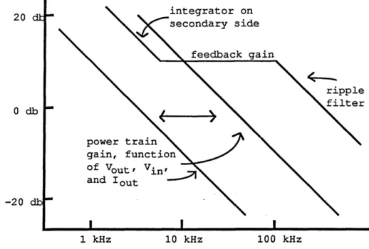
If load regulation through the isolation stage is within a few percent,
feedback from the bus voltage can provide reasonable regulation without
re-quiring isolation. Thus, "fast" feedback can be accomplished quite easily.
DC regulation can be achieved with a "slow" isolated integrator on the
out-put. The effective bandwidth of the circuit can be on the order of one fifth
of the switching frequency while an inexpensive opto-isolator can be used for
DC regulation. This simplifies the control design because fast
(>
100 kHz)isolated feedback is expensive both in dollars and complexity.
If
a P.O.L.ap-plication did not require isolation, however, the need for two feedback paths
would be eliminated.
protection can be accomplished by limiting the bus voltage. For example, if
the bus voltage becomes too large, the pre-regulator could be shut down (and
the isolation stage, too). This would allow almost instantaneous protection
without the need for a crowbar circuit.
Because both stages in a two stage converter are designed to minimize
their loss (i.e., lossless switching in second stage and only 100 m W of
induc-tive switching loss in pre-regulator) and both are optimized for their
func-tion, higher switching frequencies may be accomplished without sacrificing
efficiency. But, the frequency should only be large enough to optimize the use
of the energy storage elements without paying too large a price in switching
(boost converter) and proximity (transformer, inductor) losses. Also, other
constraints, such as the recovery time of the MOSFET body diode, limit the
maximum frequency. These constraints depend on the implementation of the
two stage design, however.
The goal of high power density is then easily accomplished, especially
considering that most converters are designed to act as voltage sources and
the output impedance of the two stage converter is significantly reduced due
to the energy storage at the high voltage bus capacitor. Instead of improving
the energy density of the capacitor by redesigning it, the circuit is designed to
take advantage of the energy storage capability. Consequently, the switching
frequency does not have to be drastically increased from what is common
today, perhaps 100 kHz, to achieve power densities in the region of 50 VV/in3
2.3
Disadvantages of Two Stage Converters
A two stage converter may require more switches, more energy storage com-ponents, and more complicated control circuitry than a single stage converter. Thus, a designer might only consider using a two stage design if the power
level is large
(>
200W).
or transient performance is important. The powerlevel of a commercial converter corresponds roughly to the cost of a
con-verter, which is on the order of one dollar per watt. For example, a full
bridge converter, which has as many primary side switches (four) as the working two stage converter, is normally used for power levels over 250 W. The full bridge converter has two high side switches which make the control
design more complicated. However, a single ended forward converter, or a
flyback converter, has only one primary side switch, is easy to control, and, owing partly to poor transformer utilization, is used for 150 W power levels or less. These converters, if designed to do so, can be paralleled, and are
therefore not limited to only low power applications. If a control
Ie
wasdesigned for the two stage converter, however, the power level one would use it at would be lower.
Chapter
3
Power Stage Design
This chapter describes the design of the power stages of the two stage
con-verter. First, the design and operation of the isolation stage is covered in
detail, particularly how lossless switching is achieved. Next, the design of
the pre-regulator, a discontinuous mode boost converter, is described,
par-ticularly how the pre-regulator is designed to meet the specifications.
3.1
Specifications
The circuit has been designed to meet the following specifications: Input Voltage Output Voltage Output Current Output Ripple Input Ripple 25
%
Load Change 35 - 60V 5V :f: 1% 50 A 50 mV p-p <5mVp-p < 4% droopSwitching Frequency 500 kHz Isolation
Soft-Start
Over- Current Protection
Over- Voltage Protection
It is designed for a telecommunication's application or a point-of-Ioad supply
in a distributed power system. The finished circuit measures 3.9" x 2.2" x
.35" unpackaged.
3.2
Isolation Stage (Push-Pull Converter)
3.2.1
Operation
at 100% Duty-Cycle
The second stage of the converter, the isolation stage, is a push-pull
con-verter operating at 100% duty-cycle. The isolation stage acts to step down
the intermediate bus voltage to the load voltage, as shown in Fig. 3.1. No
regulation is performed. The push-pull circuit has either one or the other
switch conducting at all times.
There are a number of benefits to operating at 100% duty-cycle. First,
as mentioned earlier, the voltage stress on all the components is constant
over all operating conditions (input voltage and power level). Second, the
voltage stress on the switches and rectifiers is minimized for the required
output voltage. Third, the possibility' of benign transitions, which will be
discussed in this section, allows minimal switching losses. Fourth, the core
Vout
5V
duty-cycl
e
=
100%
Figure 3.1: The isolation stage, a push-pull converter
a double ended circuit.
3.2.2
Zero-Voltage Switching
The two switch transitions in the isolation stage can cause losses. First,
when a switch is turned off, the voltage rises at its drain node while some of
the current may still be flowing down the channel. Second, when a switch
is turned on, stray capacitance at the drain node is discharged through the
channel. Also, during turn-on, the current will begin to flow through the
channel before the drain-source voltage has collapsed to zero.
The first loss mechanism, turn-off, is alleviated because the substantial
capacitance at the drain node, both from the output capacitance of the
MOS-FET and the differential mode capacitance of the transformer, acts as a
snub-her; the current flows into the capacitance rather than down the channel.
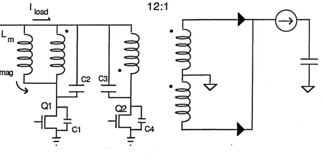
12:1
J
•
•
C2 C3I
load ----I.L
m
I
mcgFigure 3.2: Circuit diagram for transition analysis.
turn-on loss. This section describes how the switch is turned on losslessly
be-cause this capacitance is discharged, by actions inherent in the circuit, prior
to turn on.
For this analysis, assume Q1 of Fig 3.2 is conducting, the flux is
bal-anced, and the control circuit has set the output voltage to be 5 V. When Ql
is turned off, the current that was flowing through the channel of Q1 flows
instead into the junction capacitance, C1, and transformer capacitance, C2.
If the two primary winding are well coupled (Fig 3.3), the capacitance across
Q2, C3 and C4, will discharge and appear in parallel with C1 and C2.
There-fore, assuming the capacitors are linear, half of the current will be charging
C1 and 02 and half will be discharging C3 and C4.
Turning off Q1 has initiated the charging and discharging of the parasitic
"
"
Model
for leakage inductance
in push-pull transformer.
Figure 3.3: Model of isolation stage transformer
charging and discharging is continued by an LC ring, where L is the parallel
combination of the magnetizing inductance and the primary to secondary
leakage inductance, and C is the total capacitance, Ctotal=C1 +C2+C3+C4.
The energy stored in the primary to secondary leakage inductance and the
current in the magnetizing inductance drive the LC ring.
If,
for example, the magnetizing current and leakage inductance were zero,the voltage across the transformer would reach zero volts, with an RC time
constant, and stay there. When Q2 was turned on, the capacitive energy
storage, 1/2(01 + 02 + 03 + 04)V~", would be dissipated!.
If
the magnetizing current were still.zero, but the leakage inductance wasnot, the voltage would ring to a maximum value of Iload' / Lleakage/( Gtotal) V.
Thus, under full load, if the magnitude of the ring is larger than the bus
1For the converter designed, where the total capacitance is about 4 nF, Vbus is 60 V
voltage, C3
+
C4 would discharge until the body diode of Q2 clamped thering and Q2 could then be turned on losslessly. Also, because the
drain-gate capacitance of Q2, which is part of C4, is also discharged, the Miller
capacitance energy is saved, which lowers the gate drive losses. However,
because the magnitude of the ring depends on the load current, under light
enough load the ring will be sma1l2 and the resulting capacitive discharge
when Q2 is turned on will lower the circuit efficiency.
If the magnetizing current is not zero, it contributes to the initial current
stored in the leakage inductance. Therefore, the ring will attempt to reach a
va1ue of
l!,.ing =
(hood
+
ImBgnetizing) ( LmagnetizingII
Lleakage) Gtotalassuming that the output filter inductor is a current source. During the ring
the magnetizing current will be commutating to the secondary side. This
commutation may prevent the ring from continuing to the point when Q2
can be turned on losslessly, or, in other words, the value of V;ing may still be
less than Vbu6•
Choosing the proper value of magnetizing inductance can guarantee that
zero-voltage switching will take place over all value of load current. For
example, if the value of magnetizing current at the start of the LC nng
exceeds the load current, some of the magnetizing current must stay on the
AWith a leakage inductance of 400 nH and a stray capacitance of 4 nF, the impedance
primary side (Imagnetizing - I'eakage) and this will drive the ring to the point
of clamping Q2. However, even if Q2 is turned on early, a large amount of
energy will be saved because capacitive energy is stored as V2
• Thus, under
light load, most of the magnetizing current will stay on the primary side,
maintaining the lossless transitions.
Two observations: first, the circuit does not have true 100% duty cycle
because when the capacitances charge and discharge during transitions,
volts-seconds are lost3
• Second, because the body-diode of the MOSFET is used as
a voltage clamp, this MOSFET should not be made to support voltage until
most of the reverse recovery charge has recombined. These two conditions
place a limit on the maximum switching frequency. Because the reverse
recovery time for the body-diode of the 200 V MOSFET used is about 500 ns
and the transitions take about 80 ns, the operating frequency was chosen to
be 500 kHz.
3.2.3
Load Regulation
The load regulation of the isolation stage depends on a number of
fac-tors. First, during each transition, volt-seconds are lost in energizing and
de-energizing the leakage inductance. Its contribution to load regulation is
(3.1 )
3during the charging and discharging of the stray capacitances, the voltage across the
Second, the resistance and diode drop also contribute to negative load
regula-tion. Finally, the volt-seconds lost during the transitions due to the charging
and discharging of parasitic capacitances contribute to load regulation: as
the load current increases, the transition time decreases, giving an increase in
volt-seconds and positive load regulation. Thus, the isolation stage load
reg-ulation can be improved by balancing the positive and negative contributions
over the range of output current levels.
For example, assume that during a transition the capacitor is charged by
a constant current source whose value is the magnetizing current plus the
load current .. The transition time would be
dt
=
C 120 VI'oad
+
I magnetizingand the volt seconds lost per transition would be
1
volt - seconds
=
-D.tx120 V .. 2
If
the leakage inductance was 500 nH, then the volt-seconds lost per transitionwould be
volt - seconds = 2x500 nHx1'oad.
If C is chosen such that the total volt-seconds lost were made to equal at
two values of
1
,0M, in this case at 0 A and 4 A (the maximum load currentreferenced to primary side), the maximum load regulation can be made very
small. In this example, Imagnetizing = 4 A. Solving,
yields 0
=
4.4 nF. The maximum deviation in volt-seconds, according tothis model, occurs at I'oad = 1.6 A. If the transitions occurred every IJ1.s,the
voltage change would be
0.7
V, or 1%1
This model does not account for thediode drop and resistive losses, however, and is therefore overly optimistic.
If,
instead of a constant current source, a more accurate model, includingthe LO ring, is used, the calculation of the load regulation becomes more
complicated. A computer would then be used to solve the problem, whose
model would include the voltage drop across the diode and resistances to
obtain an accurate result.
3.2.4
Output Filter
If the duty-cycle were exactly 100%, and if there were no leakage inductance,
only a small, or even no, output capacitor would be needed, without any
filter inductor, to meet the output ripple specifications. However, during a
transition, ~he isolation stage passes through an instance when no energy
(load current) is being transmitted through the transformer. Without an
output inductor to sustain the load current during a transition, the load
current delivered through the transformer starts at zero amps after each
transition.
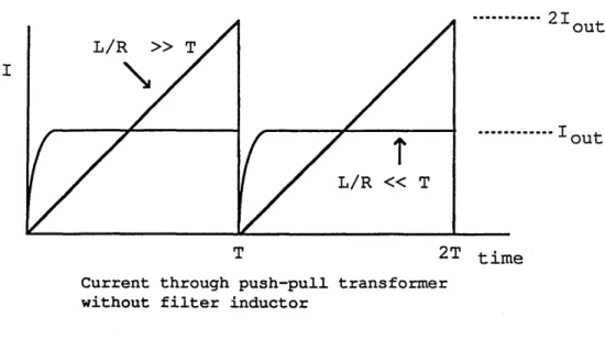
Without an output inductor, the shape of the current waveform through
the transformer depends on the ratio of the Lleakage/ Rpara:sitic time constant
I
.•••••••••. 2 I
out
... lout
T 2T time
Current through push-pull transfor.mer without filter inductor
Figure 3.4: Output current showning effect of L/R time constant
and the peak current would be twice the average. This is shown in Fig. 3.4.
On the other hand, if the L/R time constant is much smaller than a period,
the current through the transformer would be almost the same as if the
transformer had no leakage inductance. An accurate calculation of this effect
is given in [1].
At the full output current, 50 A, a 300J.LF capacitor would be needed
to provide 50 m V of voltage ripple at the output, given a 100 A peak-peak
sawtooth current waveform with a 1J.Ls period. This capacitor would cost
too much to be practical (over $300 for a ceramic capacitor at today' small
quantity pricesl). However, a small inductor, on the order of magnitude
of the leakage inductance, could aid in sustaining the load current through
each transition. The model used in determining the value of filtering
determines the current ripple:
~I
= (volt - seconds/transition)/ Lfilter.The volt-seconds lost per transition was given above as the sum due to the capacitive charging time and leakage inductance energy transfer.
A number of factors determine the size of Lfilter. As Lfilter becomes
larger, the current ripple becomes less and a smaller output capacitor is
needed. But, as Lfilter becomes larger, the transient response is degraded
because the high voltage bus capacitor becomes further separated from the
output capacitor. Therefore, the values ofLfilter and Gout depend on cost and
performance. If Lfilter became large enough (150 nH or more), which would
greatly reduce the ripple current, tantalum capacitors could be substituted for the ceramic capacitor used at the output now. The circuit now contains a 30 nH filter inductor and a 25 f.LF ceramic output cap~citor.
Because the output filter may have a large Q, tantalum capacitors are
placed in parallel with the ceramic capacitor at the output and provide damp-ing. The tantalum capacitor's impedance at the resonant frequency of the
output filter is resistive, about 100 mn per capacitor4, and four are used in
parallel. They also help the ceramic capacitors hold up the output voltage and reduce the ripple voltage. The model for the output filter is shown in
Fig. 3.6.
v
volt-seconds
dI = L filter lost volt-seconds ~ ~ time L filter Vout
Figure 3.5: Model used to determine value of output inductor
30nH
200 JlF
3.2.5
Circuit Diagram
The isolation stage (push-pull converter) is shown in Fig. 3.7. The two FETs,
Q3 and Q4, are rated for 200V and are the largest available in a TO-220
pack-age. Two transformers are placed in parallel to reduce conduction losses,
decrease the leakage inductance, lower the temperature rise
in
the cores, andlower the height of the converter (the transformers are the tallest object on
the substrate). The magnetizing inductance is chosen so that the peak to
peak magnetizing current is twice the maximum load current. This increases
conduction losses in the isolation stage's primary side by 33% at peak power
but helps to insure zero volt transitions. Ultra-low forward voltage
Schot-tky rectifiers from Unitrode, USD7520's, [23] are used on the secondary side.
These rectifiers can withstand 20V with minimal leakage (data sheet in
Ap-pendix). The drive and control circuit for the FETs is described in Chapter
4.
3.3
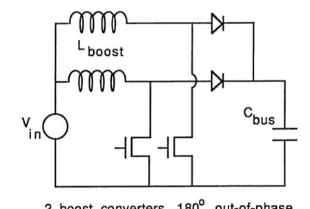
Pre-Regulator
The pre-regulator consists of two 250 kHz, 125 W discontinuous mode boost
converters in parallel and 1800 out of phase (ripple frequency at 500 kHz) that
feed into the common bus capacitor as, shown in Fig 3.8. The pre-regulator
is designed to operate with an input voltage range of 30-60
v.
The boost converter operates as follows. First, Q1 is turned on, energizing
contro~ connect~on. ~v,.. .. mot"-I
-L
C23 ~ 22nf -L- C28 ~ • .1Uf (t.nt.~um fo,..damp~ngJ outpu~ ~v. ~OA -LI
C7-~o aoou1over current protac~~on for pu.n-pu~~ c~rcu1t and sof~- ..t.rt -L ce ~ 2!5U1
-;:u
I~
~OOOv common-mod. cap 60nH eonH ov.r-vo~tag. pratect~an C2~1nq;:
f~UX ba~anc~ng c~rcu~t
bo~h Q3 .nd Q'"anou~d never be on togethe~ dead t~me can be ad,uated by .dd~ng
capac~tance to R4~. R42 D USD7!520 C~8 B.2n1' R1B
.~ow. FET turn-on
and lower P d~ •• 1n U2
~2.1 .!.
4.021< ""'l
~"'oe po~ core
C32
If----::L .
• .1uf '"=:=" ~24 l",en .... Fl2 ~ 5k R11 100k Q2 5V for log~c ch~p. D!5 NPN. SOT23 -L C20 ~ .:'ut' Bv o from traneformer 07 )1 C:":"S~~ C2B """T"-• :'U1 ~ Not ... :~33. ~!5!5.~!5e sre :..ro onm :umaer. =33 and C3~ are no~ 1n ~~e layout ~aa. tor 0: ~ro no~ pre •• nt
L boost
V
in
o
2 boost converters, 180 out-of-phase
Figure 3.8: Boost converter
rectifier into the bus capacitor. In cyclic steady state, zero volt-seconds are
applied across the inductor during a period. If the current in the inductor
reaches zero amps, the circuit has three states:
Ql
on,Dl
off;Ql
off,Dl
onj and
Ql
off,Dl
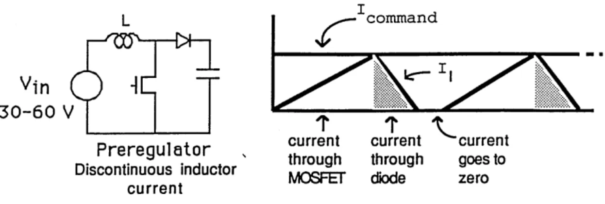
off. This condition is known as discontinuous conductionmode (DCM). Otherwise, if the current in the inductor does not reach zero amps, the converter is operating in the continuous conduction mode (CCM) and the circuit will be in only the first two states.
The CCM boost converter's inductor has a dc current and an ac ripple. The ripple is increased by making the inductance smaller. If the ac ripple is twice the dc current, the current in the inductor would start at zero amps and rise to twice the dc value. If the inductance was made any smaller, the
converter would begin to enter the DCM. Thus, the difference between a DCM boost converter and a CCM boost converter is the value of inductance,
L1, given both circuits operate at the same frequency and over the same
voltage and power range.
The CCM boost converter has a larger value of inductance than the DCM
converter. This allows the DCM boost converter to have faster dynamics than
the CCM boost converter. The DCM boost converter stores energy and then
delivers the energy to the bus capacitor each cycle, with zero joules of energy
storage in the inductor at the start of each cyele. This allows the DCM
boost converter to respond to a transient in output current or input voltage
in one period with an instant change in duty-cycle (with a small change in
output voltage) while the CCM vers.ion must accumulate volt-seconds on the
inductor over many cyeles5 to change its output current.
The CCM boost converter has a right-half plane zero which makes
control-ling it difficult. This is demonstrated, when, during a transient, an increase
in load current requires an increase in the DC current in the inductor. Q1
must remain on longer initially, to add net positive volt-seconds across L1.
The result, though, is a temporary decrease in the current delivered to the
load because the average time the rectifier conducts is decreased. The
con-trol, sensing a drop in the output voltage, must initially command the wrong
action (a further decrease in output voltage) in order to change the output
5A larger value of inductance requires more volt-seconds to change the value of its
current so that it will be able to supply it after the transient has died away6. This RHP zero makes the boost converter more difficult to control. In order to stabilize the system and achieve adequate closed loop response, both the inductor current and the output voltage needs to be fed-back to the control system. However, the DCM boost converter does not have a RHP zero and is therefore easier to control.
A DCM boost converter is used for the pre-regulator because it has a
faster response, it is easier to control, and it requires less magnetic energy
storage. Also, the large current ripple provides a larger signal for
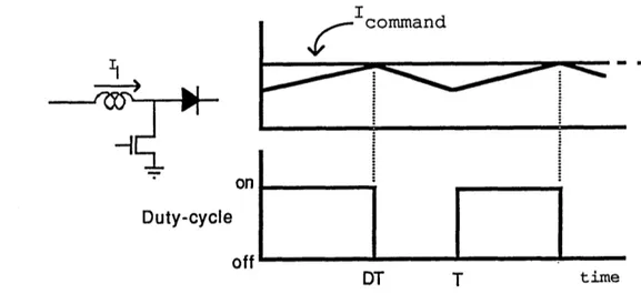
imple-menting current mode control [24]. Since the switch is turned on with zero current in the inductor, the turn-on loss is reduced to only a capacitive en-ergy discharge. Zero initial inductor current also allows turning on the switch slowly. This makes using current mode control easier because a slow turn-on reduces the current spike from the charging of the MOSFET gate which might otherwise falsely trigger the current-mode control comparator.
The DCM boost converter has detriments: it requires more capacitance
for filtering (larger current ripple), it has higher conduction losses because the rms current is larger, and it has larger turn off losses because the peak current is larger; at least twice that of the CCM converter during
turn-off. Because the pre-regulator boost converter is not transformer isolated,
however, the inductive energy loss is very small and the penalty for having 6Note that the initial and final duty cycle, before and after the transient, are the same
a larger current at turn-off (larger 1/2LP losses) does not affect the overall
converter efficiency. The I-V turn-off loss can be eliminated if the MOSFET
gate drive circuitry can turn the device off fast enough. This would force
the current to flow into the output capacitance of the MOSFET rather than
through its channel, and could be accomplished by using a MOSFET with
an integral turn-off driver [25] [26]. But, the gate drive drive circuit used in this converter cannot accomplish this so the turn-off loss is increased.
3.3.1
Designing the Pre-Regulator
In order to design the converter, the behavior of the DOM boost converter
needs to be calculated. Because the control chip has a range of duty-cycle,
the output voltage (bus voltage) and inductor must be chosen so that the
converter can meet the power and voltage specifications. The equations for
determining the design are developed next.
In cyclic steady state,
Ql
is turned on for a time DT making the currentin L rise to
When
Ql
is turned off, the current flows throughDl
for a timeVinxDT /(Vout - Vin).
Thus, the average output current is(I L,peak ) Vin D
Iout,average
=
2(V
-
1/ )out In
(3.2)
(3.3)
Slope = Vin L ~ boo~t V,
-v
Slope = bus in L II boost currentDT
currentT
time
through through MOSFET rectifierFigure 3.9:' Waveforms for understanding design equations
IS
Power -_
~~D2T
2£(
V Vout )out - Vin .
Also, the percentage of time the inductor carries current is
which must be less than 100% for DeM.
(3.4)
(3.5)
Given these equations, three conditions determine Vout and L. At
max-imum power, maxmax-imum duty cycle and minmax-imum input voltage, the same value of Land T should allow maximum power at some other smaller duty cycle when the input voltage is at its' maximum. Also, the total On-time should never exceed one and this must be checked at the maximum input
voltage. Finally, notice that the equation for power scales with Land T. Therefore L can be chosen after
v:,ut
is determined. These conditions arerepresented as
V
2 D2 ( ~ut )V
2 D2 (V
out ) in,min max TT _ 11: . = in,max TT _ TT.v out tn,mtn Vout v in,max
where Vin,min
=
30 V, Dmax=
45%, and Vin,max=
60 V. Solving yieldsD
2=
(V
out - 60) (0.45) 2 •Vout - 30 2
And, at Vin,max, the maximum On-time is made equal to 0.95.
Vout 0.95
=
D V out _ 60(3.6)
(3.7)
(3.8)
By eliminating D, ~ut equals 67 V. In the actual design, ~ut is made
slightly larger than this. The transformer has a 12:1 turns ratio, which, if
the lost volt-seconds.frequericy and diode drops are accounted for, requires
about 70 V on the bus to sustain a 5 V output.
The next step is calculating the value of L. Using Eq. 3.4, with T
=
4ILsand Power
=
125 W, one finds that L=
5.3 ILH. However, a value of 6.4 ILHwas used in the fabricated circuit. Consequently, at the lower values Vin, the
circuit cannot deliver full power.
At the larger input voltages, the circuit, if called to deliver more than
the designed power, can enter the CC1\l of operation. This does not ca.use
any control problems, however, because the energy storage in the inductor,
Crossing the boundary from DCM to CCM does not suddenly cause the control to become unstable.
3.3.2
Paralleling Converters
The converter designed for this thesis has for a pre-regulator two 125 W
boost stages in parallel, each operating at 250 kHz and 1800 out of phase.
The pre-regulator appears as one 500 kHz boost converter when calculating . voltage ripple and switching losses.
By doubling the number of switches, the current flows through twice the amount of silicon and copper. Increasing the silicon area in this manner can
be extended to three of more converters in parallel. ~f the converter has
excess conduction losses, and, perhaps, the largest MOSFET's are already
being used, this technique would solve the problem.
Paralleling has other benefits. Realizing that some of the switching losses are comprised of energy that is stored in stray inductances and capacitances and lost during each switch tran~ition, switching losses can be decreased by
using the parallel approach. For example, if two switches with resistance R
and are used in parallel and out of phase, they would have some switching
loss.
If
a switch with resistance R/2 were used instead, at the sameeffec-tive switching frequency, the switching losses would be doubled because the capacitance of this switch would be twice that of the switch with resistance