HAL Id: hal-02180620
https://hal.archives-ouvertes.fr/hal-02180620
Submitted on 11 Jul 2019
HAL is a multi-disciplinary open access
archive for the deposit and dissemination of
sci-entific research documents, whether they are
pub-lished or not. The documents may come from
teaching and research institutions in France or
abroad, or from public or private research centers.
L’archive ouverte pluridisciplinaire HAL, est
destinée au dépôt et à la diffusion de documents
scientifiques de niveau recherche, publiés ou non,
émanant des établissements d’enseignement et de
recherche français ou étrangers, des laboratoires
publics ou privés.
Gate leakage-current analysis and modelling of planar
and trench power SiC MOSFET devices in extreme
short-circuit operation
François Boige, F. Richardeau
To cite this version:
François Boige, F. Richardeau. Gate leakage-current analysis and modelling of planar and trench
power SiC MOSFET devices in extreme short-circuit operation. Microelectronics Reliability, Elsevier,
2017, 76-77, pp.532-538. �10.1016/j.microrel.2017.06.084�. �hal-02180620�
Gate leakage-current analysis and modelling of planar and trench
power SiC MOSFET devices in extreme short-circuit operation
F. Boige
a,*,
F. Richardeau
aa LAPLACE, University of Toulouse, CNRS, INPT, UPS, France.
Abstract
The purpose of this paper is to present a complete analysis of the gate leakage-current behaviour during short-circuit (SC) fault operation of 1200V SiC MOSFETs from five different manufacturers including planar and trench-gate structures. Ruggedness and gate leakage level are evaluated in function of the chip size. Finally, the gate leakage current is modelled and the robustness tested.
Corresponding author.
boige@laplace.univ-tlse.fr
Tel: +33 534 32 24 07
Gate leakage-current analysis and modelling of planar and trench
power SiC MOSFET devices in extreme short-circuit operation
F. Boige
a,*,
F. Richardeau
a* Corresponding author. boige@laplace.univ-tlse.fr Tel: +33 534 32 24 07
1. Introduction
Recently, several research efforts demonstrate that ruggedness of SiC power MOSFETs during short-circuit (SC) is, for most of devices, much lower than silicon (Si) devices, with similar rating [1]. The weakness is caused by a high short-circuit current density combined with a weak oxide and a parasitic bipolar transistor effect. Moreover, in all results, after few microsecond of SC the gate-leakage current increases significantly (few mA). In facts, this current could be monitored and possibly used to detect the fault.
In this paper, short-circuit tests were performed on six discrete-types 80m@25°C-1200V SiC MOSFETS devices including different generation-type of devices. Two generation-types (respectively C1 and C2 MOSFETs) are manufactured by CREE™ (CMF20120-16.5mm² first and C2M0080120-10.4mm² second generation), two types (respectively R2 and R3 MOSFETs) are manufactured by ROHM™ (SCT2080KE-13.6mm² second and SCT3080KE-5.3mm² third generation with a trench-gate structure) and one type (ST1 MOSFET) is manufactured by STMicroelectronics™ (SCT30N120 -13.7mm² first generation). Otherwise, the gate leakage study and the modelling are more focused on the component SCT2080KE (R2) because of its fail-to-safe destruction mode in open-circuit [1].
The proposed study is presenting an extensive study of the ruggedness of the commercials SiC MOSFET under type 1 extreme short-circuit operation. Emphasis has been put on studying the gate leakage current behaviour during SC phase and analyse the influence of the technology on this leakage. In section 2, the experimental setup and the measurement methodology is presented. In section 3, the experimental results are described and analysed by standardizing through the chips surface. In section 4, the gate-leakage current is numerically modelled in MATLAB™ and presented in function of experimental parameters. Results are discussed and
Fig. 1. Devices type 1 short-circuit test schematic. Oscillo.: Ref. Tektronix DPO4014B, BW 1GHz – 5GS/s. Probes: 2x Tek. TPP1000 300V 1GHz 3.9pF, 1xTek.TPP0850 800MHz 1000V 1.8pF – 300mV offset compensation on Vbuffer – with fuse and DUT– Supply
driver THB3-1215 – probes propagation time are compensated – aselfic coaxial shunt – CMS Schurter fuses.
Fig. 2. Experimental waveforms during short-circuit of R2. ( ; ; ;
; R2) (a) gate-source voltage. (b) Drain current (saturation current) and drain-source voltage.
the robustness of the model validated. Such a model is promising for circuit-type simulator such as PSPICE™ software.
2. Experimental setup and measure protocol
The aim of the measures is testing the components in an extreme mode but without destruction. The device under test (DUT) is turned-on across a voltage source and through a polypropylene-capacitors tank providing the high- current pulse which is only limited by the device resistance. An increment of the short-circuit duration is carefully realised and stopped before the device failure. Fig. 1 shows the schematic of the proposed experimental set-up. The gate turn-on bias ( ) is
adjustable (18V–21V) as well as the blocking bias ( ) (-5V–0V) and the drain-source voltage
( ) (0V– 600V). Measured data are saved and
post-processed with MATLAB© and filtered (Gaussian filter σ=10). The gate current is calculated with the voltage drop across the gate resistor.
3. Experimental results
3.1. Evaluation of R2 behaviour
In this section, the influence of experimental parameters ( ) on SiC MOSFET
short-circuit behaviour is depicted. The SC behaviour for different of R2 is given Fig.
2. The phenomena can be divided into 3 sequences: in Seq. 1, the saturation current ( ) rises quickly.
Then, in Seq. 2, decreases along with the
temperature rising and gate leakage current dynamic is not temperature dependant. Finally, the Seq. 3 is defined by the moment where the gate-voltage is subject to a great reduction due to the gate leakage current surge through the external gate-resistor. This current is most likely caused by a Fowler-Nordheim phenomena (field electron emission) [2], [3]. Practically, Seq.3 starts at half of destruction time (TSC) for R2 device.
3.1.1 Buffer bias influence
During this Seq. 3, the temperature inside the chip is assumed to be very important [4] and the results Fig.3 (a) shows that the gate-leakage current dynamic is highly dependent on . Hence,
the dynamic origin is a combination between electrostatic and thermal effects. Furthermore, Fig. 3 (b) shows that the gate current leakage runaway, which define Seq. 3, starts always at the same energy level (5.9J/cm²) named .
3.1.2. Drain-source Influence
Fig. 3. (a) for different & .(b) & . (c) &
.
During Seq. 1 and 2, the drain-source voltage has no influence on the gate current because the die temperature is low and the gate-leakage is mostly governed by electrostatic effects. Conversely, in the Seq. 3, the dynamic is strongly depending of this parameter. Indeed, the increase leads to higher
power losses and temperature increases. It is noteworthy that the leakage no longer exists for
for any . (Fig 3 (c)) and no
longer exists for for any .
To conclude, gate leakage current starts because of the important junction temperature but its dynamic remains influenced by electrostatic factors.
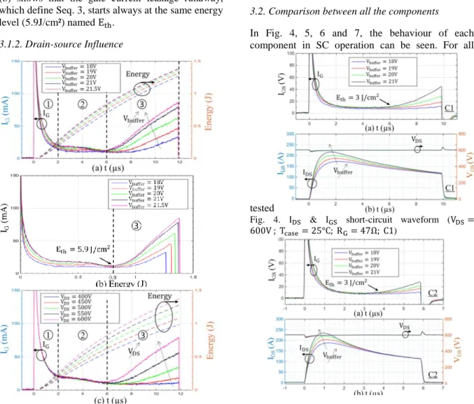
3.2. Comparison between all the components
In Fig. 4, 5, 6 and 7, the behaviour of each component in SC operation can be seen. For all
tested
Fig. 4. & short-circuit waveform (
Fig. 5. & short-circuit waveform ( ; ; ; C2)
components, the testing time is 2µs lower than the failure time ( ) to avoid the device failure. The
Fig. 8 summarise the experimental results standardizing through the chips surface ( ).
Indeed, even if the experimental conditions are the same and the components have similar rating, the components and gate leakage current are
different. These differences can be explained by the surface difference and the technologies used as explained in the following.
• CREE: the two components are V-DMOSFET with an optimization of the doping layers between the generations [5]. This modification increased the saturation current density ( ) by 77% which
permited a reduction of by 37% with an identical . However, increasing and
decreasing lead to a faster chip self heating and
it is decreasing by 30%. Indeed, the literature of the destructive tests gives a of 12μs for C1 and
of 8μs for C2 [1]. In terms of gate leakage current density
Fig. 6. and short-circuit waveform (
)
Fig. 7. and short-circuit waveform (
( ), C1 and C2 are equal, due to the lower size of
C2. Finally, the is the same for C1 and C2 at
3J/cm², which means that the two generations use the same oxide thickness and technology.
• ST: One generation is available today and no documentation about the technology have been published. However, with and with a similar
to those of C1 and C2, the oxide technology is assumed to be similar to that of C1 and C2. Moreover, the ST transconductance is higher than others ones which implies a high (max 3
kA/cm²). This results in a very low short-circuit ruggedness (<6μs) and so requires a faster protection circuit.
• ROHM: between the R2 and R3, the technology changed. Indeed, R2 is a V-DMOSFET with deep P-well shielding [3]. This technology has the advantage of protecting the gate oxide from the high electric field in the drift layer. Consequently, the and
are higher than those of C1, C2 and ST. On the other hand, R3 is a trench vertical MOSFET with deep P-
well shielding [6]. This technology has the advantage of suppressing the JFET regions and allow a higher cells density. These characteristics imply a
increase by 150% and allow a chip size reduction by 61% with the same rating. Moreover, as the previous generation, the deep shielding is protecting the gate oxide. As a result, R3 can sustain a higher dissipated energy density inside the chip by 23%. For R3, the
is 33% lower than the one of R2 and the is
27% greater. Concerning TSC capability, R2 shows a
short circuit robustness greater than 10μs, as a standard IGBT die. In the end, the combination of the higher and the chip size reduction on R3 lead
to a , which is 50% lower than R2.
In order to protect the components, the use of the gate leakage current seems to be interesting for the component R2 with a leakage start around 5µs and a of 14µs. However, some components
present a very low short-circuit ruggedness (<6μs) with a leakage starting around 3-4µs which is quite challenging. The protection circuit design is still in study.
4. Gate-leakage Modelling
Based on experimental results developed in section 3.1 for R2, a behavioural leakage current model was developed. The aim of this model is to accurately describe the component behaviour in order to embed it into a MOSFET model in SPICE™-like software to help the protection circuit development.
In order to limit the complexity, the model is not directly physical and depends on 3 parameters:
and E, the energy dissipated inside the chip
during the SC, which is an image of the junction temperature growth. Nevertheless, at this stage, the proposed method is only valid for a fixed initial junction temperature. The model is going to be valid
from the gate leakage energy threshold only ( ).
With associated validity domain:
. Finally, the model is going to be used as a “block” ready to use into a usual MOSFET gate model as shown Fig. 9
4.1 Model
A polynomial surface (1) was chosen and the parameters were estimated with MATLAB™ to model the gate current-surge variation in function of
and dissipated energy ( ).
(1)
(2)
(3)
( ) are the estimated factors.
However, variation is not yet added in the
model. To do that, factors ( ) are,
themselves, estimated for different VDS bias and
pre-calculated in a table. The coefficients are presented table I. It appears that the factors vary linearly along .
I. Estimated factors function of
4.2 Results and robustness of the model
In order to determine the model robustness, two tests were made. Firstly, the proposed model was compared with experimental results which are different from those used to estimate the model parameters (Fig. 10 (a)). Secondly, the proposed
model was compared with data obtained from another
Fig. 9. Electrical SiC MOSFET gate model. In black line, the classical MOSFET model in gate-side representation. In red line, features proposed in this article.
R2 component (Fig. 10 (b)). In conclusion, the proposed numerical model is validated and is robust in its validity domain. Moreover, the method was performed a second time for the component C1. The results, in Fig. 11, clearly shows that this method is generic and can be adapted for other component than R2 (coefficients values are not displayed).
6. Conclusion
The results confirm the presence of a gate-leakage current runaway in short-circuit operation of a wide power SiC MOSFET devices range. This current has the advantage to have a large amplitude and to be easily measurable. Specific indicators were introduced such as the gate-current density and the energy density threshold of the gate-current runaway to compare devices. These criterions appear to be salient to define the robustness of the devices gate and an image of the gate technology. It was also confirmed, for C2, R3 and ST1 devices, that the short-circuit robustness was reduced to a few microseconds of , with a low energy density. However, the R3 trench-gate structure implies an important saturation-current density but with a better gate robustness. Finally, a relation between electrostatic and thermal coupled effects has been shown. All these elements allowed the implementation of a representative and robust model into a circuit-type software such as LT/PSPICE™ and can be used in order to design the future protection circuits. Finally, the junction temperature dependence could be added into the modelling method in the future work.
Acknowledgement
This research work received financial support from
Fig. 10. Model (red lines) and experimental (blue lines) results. (a)Results obtained with testing data set from the same device. (b)Results obtained with test data from another device.
Fig. 11. Model (red lines) and experimental (blue lines) results for a large set of training data for another
component such as C1.
the French National Research Agency (ANR). Project name: HIT-TEMS
References
[1] C. Chen et al., ‘Study of short-circuit robustness of SiC MOSFETs, analysis of the failure modes and comparison with BJTs’, Microelectron. Reliab., vol. 55, no. 9–10, pp. 1708–1713, août 2015.
[2] K. Roy, et al., ‘Leakage current mechanisms and leakage reduction techniques in deep-submicrometer CMOS circuits’, Proc. IEEE, vol. 91, no. 2, pp. 305– 327, février 2003.
[3] T. T. Nguyen, et al., ‘Gate Oxide Reliability Issues of SiC MOSFETs Under Short-Circuit Operation’, IEEE
Trans. Power Electron., vol. 30, no. 5, pp. 2445–
2455, mai 2015.
[4] Z. Wang et al., ‘Temperature-Dependent Short-Circuit Capability of Silicon Carbide Power MOSFETs’, IEEE Trans. Power Electron., vol. 31, no. 2, pp. 1555–1566, février 2016.
[5] J. Casady, ‘Power products commercial roadmap for SiC from 2012-2020’, CREE, 2014.
devices with ultra-low ron’, in Electron Devices
Meeting (IEDM), 2011 IEEE International, 2011, p.