Publisher’s version / Version de l'éditeur:
Vous avez des questions? Nous pouvons vous aider. Pour communiquer directement avec un auteur, consultez la première page de la revue dans laquelle son article a été publié afin de trouver ses coordonnées. Si vous n’arrivez pas à les repérer, communiquez avec nous à [email protected].
Questions? Contact the NRC Publications Archive team at
[email protected]. If you wish to email the authors directly, please see the first page of the publication for their contact information.
https://publications-cnrc.canada.ca/fra/droits
L’accès à ce site Web et l’utilisation de son contenu sont assujettis aux conditions présentées dans le site LISEZ CES CONDITIONS ATTENTIVEMENT AVANT D’UTILISER CE SITE WEB.
New Journal of Physics, 21, 3, pp. 1-13, 2019-03-15
READ THESE TERMS AND CONDITIONS CAREFULLY BEFORE USING THIS WEBSITE.
https://nrc-publications.canada.ca/eng/copyright
NRC Publications Archive Record / Notice des Archives des publications du CNRC :
https://nrc-publications.canada.ca/eng/view/object/?id=ebfc8106-233e-4d84-83c1-21b58fe96775
https://publications-cnrc.canada.ca/fra/voir/objet/?id=ebfc8106-233e-4d84-83c1-21b58fe96775
NRC Publications Archive
Archives des publications du CNRC
This publication could be one of several versions: author’s original, accepted manuscript or the publisher’s version. / La version de cette publication peut être l’une des suivantes : la version prépublication de l’auteur, la version acceptée du manuscrit ou la version de l’éditeur.
For the publisher’s version, please access the DOI link below./ Pour consulter la version de l’éditeur, utilisez le lien DOI ci-dessous.
https://doi.org/10.1088/1367-2630/ab03da
Access and use of this website and the material on it are subject to the Terms and Conditions set forth at
Quasi non-diffractive electron Bessel beams using direct phase masks
with applications in electron microscopy
PAPER • OPEN ACCESS
Quasi non-diffractive electron Bessel beams using direct phase masks
with applications in electron microscopy
To cite this article: Simon Hettler et al 2019 New J. Phys. 21 033007
View the article online for updates and enhancements.
New J. Phys. 21 (2019) 033007 https://doi.org/10.1088/1367-2630/ab03da
PAPER
Quasi non-diffractive electron Bessel beams using direct phase
masks with applications in electron microscopy
Simon Hettler1 , Lukas Grünewald1 and Marek Malac2
1 Laboratory for Electron Microscopy, Karlsruhe Institute of Technology, Engesserstrasse7, D-76131 Karlsruhe, Germany 2 NRC-NANO, 11241 Saskatchewan drive, Edmonton, Alberta, T6G 2M9, Canada
E-mail:[email protected]
Keywords: electron-beam shaping, non-diffractive electron beams, phase mask, electron microscopy Supplementary material for this article is availableonline
Abstract
Electron-beam shaping opens up novel imaging possibilities in electron microscopy (EM). The
implementation of a phase or amplitude mask in the condenser lens system allows the generation of
electron beams with various shapes. Non-diffractive Bessel beams (BBs) are of interest for numerous
applications due to their extraordinary large depth of focus. We present an experimental
demonstration of single high-intensity quasi non-diffractive electron BBs generated by direct phase
masks (PMs). The PM fabrication by focused ion beam is optimized using custom scan routines. The
propagation of the electron beam after transmission through several PMs is analyzed in detail. A sub
nm-sized non-diffractive electron beam is realized in the object plane of a transmission electron
microscope. The experiments agree well with simulations and a route towards a beneficial application
of non-diffractive electron beams in EM is discussed.
1. Introduction
Shaping the electron beam for novel applications in scanning transmission electron microscopy (STEM) has attracted tremendous interest since the first experimental observation of an electron vortex beam, i.e. a beam carrying orbital angular momentum [1]. Beam shaping is typically achieved by using phase masks (PMs) or
amplitude masks (AMs) fabricated using a focused ion beam (FIB). The masks influence the illuminating electron plane wave in a way that the desired electron beam amplitude and phase profile is realized in a plane below the mask. One of the most popular types of beam-shaping masks is the holographic mask whose shape is calculated from a superposition of the desired target wave function and a reference wave, e.g. a tilted plane wave. The hologram is then either transfered in a 3D structured electron-transparent thin-film membrane
(holographic PM), where the thickness variations are linked to the desired phase profile, or the hologram is binarized and structured into an obstructing aperture (holographic AM). One drawback of such holographic masks is the generation of multiple electron beams which hinders application as the desired beam exhibits a low intensity and has to be separated from the remaining beams. Direct PMs, which produce a single, high-intensity, electron beam with the desired shape are therefore better suited for practical application [2–4]. Of particular
interest are programmable PMs which are not limited to a specific beam shape [5].
In addition to electron vortex beams, which have been intensively studied by numerous groups [6–10], beam
shaping has been applied to create Airy [11], Bessel [12,13] or arbitrary beam shapes [4] and also to correct for
aberrations [14]. Among these, (quasi) non-diffractive electron Bessel beams (BBs) are promising to find an
application in probe forming for various STEM techniques. Non-diffractive beams have been proposed in light optics by Durnin [15] and were realized in an electron microscope only recently using holographic PMs [13],
nano-structured slits [16,17] or a magnetic material [18]. The beam profile of BBs is given by a Bessel function
which exhibits radial symmetry and whose shape is, at least in theory, constant upon beam propagation, i.e. the beam is non-diffractive. In the experiment, the use of a finite aperture limits the non-diffractive property to a specific propagation length zmaxalong the beam path beyond the beam-shaping mask. For typical microscopes OPEN ACCESS RE CE I VED 29 August 2018 RE VI S ED 15 December 2018 A CC E P T E D FO R P UB LI C A T I O N 1 February 2019 P UB L IS H ED 15 March 2019
Original content from this work may be used under the terms of theCreative Commons Attribution 3.0 licence.
Any further distribution of this work must maintain attribution to the author(s) and the title of the work, journal citation and DOI.
and state-of-the-art structuring possibilities, zmaxis in the range of a few cm to m, being sufficiently large to be
used as illuminating beam in STEM. The major advantage of a BB is the extraordinary high depth of focus (DOF), which is significantly higher than in conventional STEM where the DOF is dependent on the convergence angle and typically is in the range of a few tens of nm and even lower for aberration-corrected probes [19]. Additionally, BBs exhibit a self-reconstructing property which implies that their original beam
profile is (partially) restored after a scattering event. Both, the self-reconstructing property and the high DOF makes imaging with BBs of thick specimens and in STEM tomography highly promising [20,21]. In fact, BBs
benefit modern fluorescence light microscopy [22,23].
In this work we fabricated direct PMs to generate single BBs with a high intensity for application in EM. The PM fabrication is optimized to obtain high quality smooth masks. The electron-beam evolution after
transmission through the PM is analyzed in detail by a low-magnification (LM) setup in a transmission electron microscope and the experimental results agree well with corresponding simulations. PMs installed in the condenser lens system yield sub nm-sized BBs in the object plane of the microscope where the sample is placed. Possible routes leading to an application are discussed.
2. Fabrication of a PM
The PM fabrication starts with a Si wafer in (100) orientation coated with low-stress silicon nitride (in the following denoted as Si3N4)on both sides (Microchemicals GmbH, Ulm, Germany). The backside Si3N4layer is
patterned using photolithography and reactive ion etching so that a following KOH wet etch results in Si3N4
membranes with a size of 100×100 μm2. The membranes are arranged on dodecagonal chips imitating round TEM grids with 3mm diameter. Pt apertures (diameter 10–50 μm) are then fabricated in a second
photolithographic step followed by physical vapor deposition of a Cr/Pt layer (3.5/150 nm) and a lift-off process. The individual chips can be separated by manual fracturing.
Instead of fabricating the membranes in-house, commercially available TEM grids with Si3N4membranes
can also be used. However, then the Pt apertures cannot be fabricated by a lift-off process and focused-ion-beam milling has to be applied. During the FIB milling of the round aperture in the deposited Pt, the roughness of the membranes is increased due to the crystallinity of the Pt layer. Additionally, the fabrication is serial and thus rather time-consuming. A 5 nm thick amorphous carbon layer is deposited on the backside of the obtained membranes by carbon thread evaporation (MED020, Leica Microsystems) to reduce charging during FIB milling and in TEM. The PM structure is finally milled into the Si3N4membrane with a Helios G4 FIB system
(Thermo Fisher Scientific) using a beam current between 40 and 260 pA.
The thickness profile T of a direct PM creating a single BB is given by equation (1)in dependence of the cylindrical coordinates r and j [24]:
j = + - p + j <
( ) [ ( )] ( )
T r, t0 ta 1 cos 2 rkr m ;r D. 1
The offset thickness t0is given by the remaining thickness of the membrane and 2tais the amplitude between
minimum and maximum thickness of the structured profile. T is present only within the aperture diameter D. The parameter m defines the order of the resulting BB and introduces an orbital angular momentum to the electron beam. In this work we focused on BBs of zeroth order, i.e. m=0 implying T is rotationally symmetric and describes concentric circles. The Bessel frequency krdetermines the pitch between the structured circles and
the properties of the resulting BB. The thickness profile T leads to the phase profile Φ of an electron plane wave transmitted through the PM which depends on the interaction constant σ and the mean inner potential VMIPof
Si3N4:
s
F( )r = T r V( ) MIP. ( )2
Of course, Si3N4is not a pure phase object but alters the amplitude of the electron wave as well. Electrons
scattered to higher angles in the PM are absorbed by apertures or contribute to the background signal of the resulting BB. In simulations conducted in this work we use a simple model of a total mean free path λmfp,
including elastic and inelastic scattering, to calculate the amplitude damping of the electron wave. λmfp
corresponds to the thickness of the PM material at which the fraction of unscattered electrons has decreased to
e
1
after propagation through the PM. In our approach, the amplitude A of an illuminating plane wave (A0=1) is
then damped to AT=exp(−T/λmfp)depending on the thickness T of the PM. A more accurate consideration
would require multi-slice simulation of the wave after transmission through the PM but is not needed as our approach gave good agreement with the experiment.
To transfer the desired thickness profile in the Si3N4membrane in an optimum way, a stream file is created
which determines the FIB path and dwell time. In case of high kr, the stream file starts with a single point in the
center of the PM followed by vector-written circles with linearly increasing radius. The FIB is not blanked in between the circles. The distance between the circles is given by 1/krin order that only the deepest parts of the
structures are actually irradiated with the FIB. The FIB dwell time was chosen to be between 50 and 100 μs, depending on the size of the PM. To ensure a similar depth of the central spot compared to the surrounding circles, the corresponding dwell time is increased by a factor of 5. The whole path is milled approximately 30 times with each pass being rotated by an offset angle. In this setup, redeposition effects are minimized and a homogeneous structure is achieved as shown in the SEM image in figure1(b). The actual form of the depth profile is defined by the FIB beam profile and slightly differs from the desired sinusoidal form (equation (1)).
For kr<5 μm−1, gray scale milling is applied, meaning that the distance between the structured circles is
fixed and the dose for each circle is calculated by equation (1). Figure1shows SEM and cross-section TEM images of two example PMs. The TEM images reveal the implantation of Ga in the Si3N4up to a depth of
approximately 35nm. The presence of Ga will influence VMIP. However, the thickness of the Si3N4+Ga layer is
constant in the area of the PM and only affects the offset phase f0=σt0VMIP(Si3N4+Ga) and can therefore be
neglected in the simulations. The penetration depth of Ga in Si3N4also determines the minimum offset
thickness t0as the milling rate is drastically increased once a considerable fraction of Ga ions penetrate through
the PM. For PMs with low krvalues, the offset and amplitude thickness are determined by cross-section TEM to
2ta=74 nm of Si3N4and t0=35 nm of Si3N4+Ga.
3. Properties of electron BBs
A PM with kr=5 μm−1and D=10 μm is inserted as specimen in a FEI Titan 80-300 (Thermo Fischer
Scientfic) operated at 300 kV to analyze the properties of the resulting BB. The LM mode with a slightly excited objective lens (OLs) (4%–5%) is used to trace the evolution of the electron wave after transmission through the PM by defocussing the diffraction (i.e. the first intermediate) lens. The beam profile evolution is imaged with a Gatan Ultrascan CCD camera controlled by a DigitalMicrograph script. Adjustment of the rotation center and both, objective and diffraction, stigmators is crucial to minimize artifacts in the imaging process. As it is not possible to simultaneously correct for astigmatism in the whole necessary range of diffraction lens excitation, slight distortions are still visible in the acquired TEM images.
Figure2shows six example images of an acquired image series of the electron-beam evolution with in total 341 images and a defocus range of 0–340 mm. The exposure time of each image was altered to keep the maximum count number at approximately 4000 per pixel and the image contrast was adjusted to improve feature visibility. A movie of the entire electron-beam evolution as function along z can be found in
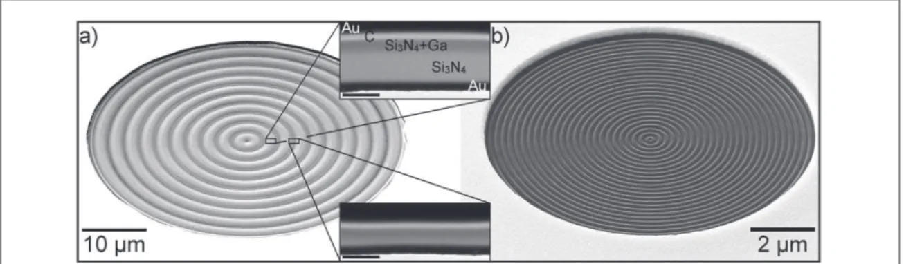
Figure 1. Scanning electron microscopy (SEM) and TEM images of two PMs with aperture diameters and Bessel frequencies krof (a)
50 μm and 0.4 μm−1and (b) 10 μm and 5 μm−1. The PMs are tilted by 52° resulting in the elliptical appearance of the round
apertures. (a) The TEM images show cross-sections of the thin and thick regions of the PM and reveal the layered structure consisting of protective Au and C layers and Si3N4with and without implanted Ga. Scale bars in insets 100 nm.
Figure 2. Example images of the electron-beam evolution after transmission through a PM (kr=5 μm−1, D=10 μm) for a
diffraction lens defocus of (a) 1, (b) 33, (c) 82, (d) 148, (e) 152 and (f)274 mm. The beam profile evolves into a Bessel-type function shortly after transmission through the PM and retains its profile up to a propagation distance z≈230 mm.
3
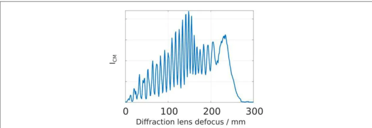
supplementary movie 1stacks.iop.org/NJP/21/033007/mmedia. A suitable method to display the electron-beam evolution in a more simplified way is to measure the intensity of the central maximum ICMin each image.
Figure3shows the evolution of ICMfor the acquired image series revealing an oscillatory increase up to a
diffraction lens defocus of around 230 mm before the intensity sharply decreases.
The second image of the series is displayed in figure2(a) and shows the electron wave 1 mm after transmission through the PM. Concentric rings are clearly visible but a central maximum is not observed because a BB has not yet formed. In the image at a diffraction lens defocus of 33 mm, corresponding to the third maximum in figure3, the electron wave is similar to a Bessel function of the first kind and 0th order which can be recognized by the central maximum of high intensity and the surrounding rings with decreasing intensity (figure2(b)). The shape of the Bessel function is then preserved upon propagation as visible in figures2(c)–(e). This preservation of the shape of the electron beam is called the non-diffractive property. While figures2(a)–(d) correspond to local maxima in figure3, the image acquired at 152 mm (figure2(e)) depicts the wave at a local minimum where the central maximum vanished and its intensity shifted to the first ring. This shows that although the overall Bessel-type shape persists upon propagation, the intensity distribution is subject to change.
The electron wave is quasi non-diffractive as the shape is only preserved up to a maximum propagation distance zmax. Figure2(f) shows an image of the electron beam outside the non-diffractive range (>zmax)which is
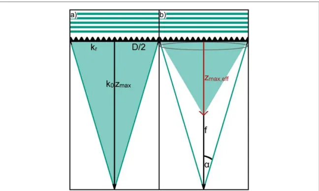
not described by a Bessel function anymore. The value for zmaxcan be estimated from a simple geometric
consideration (figure4): = ( ) z MDk k 2 r 3 max 0
zmaxdepends on the diameter of the PM D, the electron wave vector k0and the Bessel frequency kr. Figure4
shows a sketch of the determination of zmaxwithout (figure4(a)) and with an additional lens (b). The presence of
a lens can cause a (de-)magnification of the electron beam and affects the effective value of zmaxwhich is reflected
by the magnification factor M in equation (3)and can be inferred from figure4(b). Due to the weakly excited OLs, the space behind the PM is not completely field-free. Consideration of the experimental parameters D=10 μm, kr=5 μm−1and an electron energy of 300 keV results in zmax=500 mm. By comparison with the
experimentally determined value of zmax=230 mm, M can be estimated to ≈0.5 for the applied diffraction lens
defocus. The demagnification is not constant but slightly changes with the varying excitation of the diffraction lens (M=M(ILens)). This is reflected by a minor decrease in size of the BB with increasing diffraction lens
defocus (figures2(b)–(e)). The effect of a focusing lens on the electron-beam evolution is further analyzed later. The experimental results obtained on the electron-beam evolution by analysis of the PM using the LM mode in figure3in TEM agree well with those reported in literature [12,13,15,24,25].
Instead of using the diffraction lens to change the effective propagation distance between specimen and image plane, we also studied the propagation of BBs with different krfor a fixed propagation distance. The
experiment was performed by inserting the PM (D=50 μm) above the first condenser lens in a Hitachi HF-3300 (see figure7)and turning off all lenses except for the last projection lens which was used to magnify the propagated BB onto a Gatan Ultrascan 1000 camera. Figure5shows the obtained results and reveals that due to the different values of krand thus zmax, the BBs are observed in different states. While the BB generated by PMs
with low kr(a), (b) have only propagated a small fraction of zmax, the BB with kr=1 μm−1has already
propagated a larger fraction of zmax. For kr=2.5 μm−1(e), the propagated distance is almost far enough to reach
the Fraunhofer regime of the PM. Figure5(c) shows an image of a BB obtained from the identical PM as in (b)
Figure 3. Experimentally observed dependence of the central maximum intensity ICMon the diffraction lens defocus. The intensity
Figure 4. Geometrical estimation of the maximum propagation distance zmaxof a BB after a PM (a) without and (b) with a lens. (b) A
focusing lens with focal length f leads to a convergence semi angle α and a demagnification of zmaxand of the beam size.
Figure 5. Images of BBs generated by PMs with different krand identical propagation distances between PM and image plane acquired
using a Hitachi HF-3300. Due to the different zmax, the beams are in different states: while the BB with low kr(a), (b) are still in the
Fresnel regime, the BB for kr=2.5 μm−1(e) is already close to the Fraunhofer regime. (c) The shape of the BB is preserved after
propagation through matter.
5
but which has propagated through a test specimen (Grating replica, TedPella Prod. No. 607) inserted in the sample plane of the microscope. The shape of the BB and the edge of the sample grid bars are visible.
4. Generation of BBs in the sample plane
In this section we present BBs generated in the sample plane by implementation of PMs in the condenser lens system of two different microscopes. The effect of the PM positioning and the lens settings on the BBs are assessed. A comparison of an acquired image series with simulations allows to reconstruct the phase profile of the PM.
4.1. PM in C2 condenser aperture
A PM with a diameter D=10 μm and kr=5 μm−1was inserted in the C2 condenser aperture of a FEI Titan
transmission electron microscope. In conventional electron microscopy (EM), the condenser lenses are adjusted in a way that the specimen is either illuminated with an image (plane wave, TEM) or the back focal plane
(focused probe, STEM) of the C2 aperture. The BB evolves in the Fresnel regime of the PM (figure4)and thus both modes are not applicable to generate a BB in the specimen plane. In the Nanoprobe mode of the
microscope, the effective propagation distance of the BB between the PM and the specimen plane can be defined by the C3 lens excitation (’Brightness’). Supplementary movie 2stacks.iop.org/NJP/21/033007/mmediashows the BB evolution from image to back focal plane acquired by recording TEM images of the BB for varying C3 lens excitations. An increasing demagnification with time (with C3 lens excitation and effective propagation
distance) can be observed.
Figure6shows an image of a BB at low (a) and high magnification (b) taken close to zmax. The BB exhibits
numerous rings (nrings= D ·kr=25
2 )and a central maximum with a full-width at half maximum of 4 Å.
Although the central beam diameter is small, the intensity in the central maximum represents only a small fraction of the overall beam intensity. In fact, the reduced intensity in the central maximum is an intrinsic feature of non-diffractive beams and the intensity is approximately given by 1/nrings. This leads to a lower
signal-to-noise ratio if applied in STEM as the high-resolution signal stemming from the central maximum is weak compared to the contribution from the surrounding rings. Additionally, the aperture diameter D=10 μm is small compared to typical STEM apertures with diameters between 50 and 150 μm meaning that the overall intensity is small. These effects make STEM imaging with the beam displayed in figure6not beneficial.
A comparison between the experimentally obtained beam size of 4Å with the size expected from the PM parameters without a focusing lens allows to determine the demagnification. The theoretical beam size can be calculated from the first zero of the Bessel function which lies at »d
k
2
rwhich amounts to 0.4 μm for the
implemented PM with kr=5 μm−1. The achieved demagnification thus is 1/M=1000.
To increase both the overall intensity and the relative intensity of the central maximum, we chose to increase the PM diameter while simultaneously decreasing krand thus nrings. As this leads to larger sizes of the central
Figure 6. Example TEM images of a BB acquired in the Nanoprobe mode of a FEI Titan microscope showing (a) an overview of the whole BB generated by a PM with kr=5 μm−1and (b) the central maximum (diameter=4 Å) of the same BB.
maximum, the demagnification achievable by implementation of the PM in the C2 aperture is not sufficient to generate reasonably small central beam sizes. Therefore the next section contains the results obtained from an implementation of respective PMs above the C1 condenser lens of a Hitachi HF-3300.
4.2. PM in C1 condenser aperture
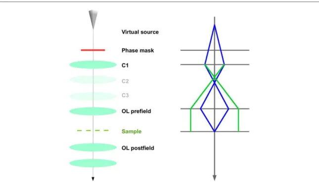
Figure7shows a schematic drawing of the electron-optical setup of the Hitachi HF-3300 with cold field emission source operated at 300 keV used for the experiments. We implemented a PM (D=50 μm, kr=0.4 μm−1)in an
aperture just above the C1 lens and used the C1 lens and the OLs prefield to generate a BB at the sample plane. In this setup we achieved a high demagnification at a moderate convergence semi angle α. The C1 lens excitation can be used to either obtain an image (high excitation, green lines in figure7)or a diffraction pattern (low excitation, blue lines) of the PM in the sample plane. As the BB evolves in the Fresnel regime between image and diffraction plane, the C1 lens excitation is adjusted in between these excitations to obtain a BB in the sample plane.
In this setup the physical distance dphysbetween PM and sample is fixed. By changing the C1 lens excitation,
the effective propagation distance deffof the BB between PM and sample plane can be expressed by equation (4):
= = -( ) ( ) ( ) · ( ) ( ) d I d M I M I c I I 4 eff C1 phys C1 C1 demag C1 C1,BFP
IC1is the C1 lens excitation, IC1,BFPis the C1 lens excitation for which a diffraction pattern of the PM is
observed, and M(IC1)is the demagnification of the PM in the sample plane in dependence of IC1. M(IC1)is
expressed by means of a fitting constant cdemagwhich is determined by measuring the demagnification of the PM
in the sample plane in dependence of IC1.
We acquired an image series of the generated BBs with IC1being varied between image plane and BFP of the
PM. The BBs were recorded using the conventional TEM mode of the imaging lenses, a Gatan Ultrascan 1000 camera and MAESTRO scripting [26]. The movie of the image series can be found in supplementary movie 3 stacks.iop.org/NJP/21/033007/mmedia. Figure8shows four characteristic BBs taken from the series. A BB observed close to the image plane is depicted in figure8(a) which reveals a bright maximum with a diameter of ≈5 Å surrounded by rings as expected for a Bessel function of 0th order and first kind. The image displayed in figure8(b) reveals a BB with a central minimum obtained for a slightly lower C1 lens excitation which is however still in the Fresnel regime of the PM. The BB with the highest intensity of the central maximum is shown in figure8(c). Due to the larger demagnification at this plane, the distance between the central maximum and its surrounding rings is strongly decreased compared to figures8(a) and (b). Additionally, minor distortions are visible in the image, which could be attributed to aberrations, the fact that the PM was slightly tilted relative to the incident beam, imperfections in the PM structure and also to a high value of fa(see following section). The
Figure 7. Sketch of lens settings used to generate BBs in the sample plane of a Hitachi HF-3300.
7
diffraction pattern of the PM (figure8(d)) closely resembles the BB from (a) but exhibits a more pronounced central maximum. An estimation of the demagnification in this setup yields 1/M=104.
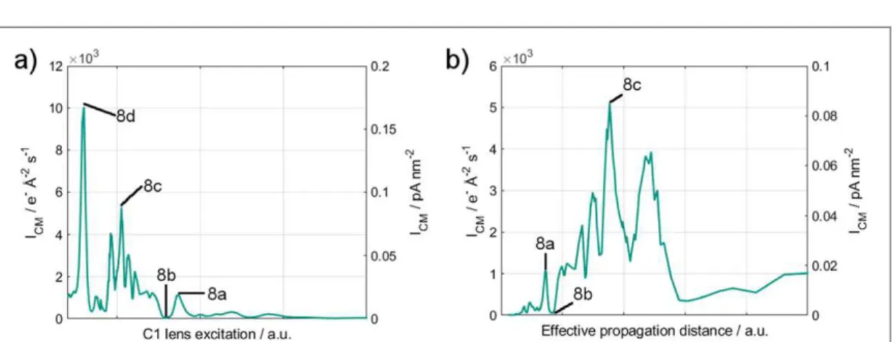
Similar to the LM setup (figure3), we determined ICMof the BB in e−per Å 2
s which can be plotted in dependence of IC1(figure9(a)) as well as of deff(b), which is calculated with the help of equation (4). As the
physical distance dphysbetween PM and sample plane is not exactly known, the calculation of deffis only
qualitative. The values of IC1for which the images in figure8were acquired are marked at the respective values of
IC1and deffin figure9. The BFP of the PM can be recognized by the highest peak at low IC1(figure9(a)) which is
not plotted in (b) as it is located at very high deff. While the dependence of ICMon IC1can be described as
reciprocal (figure9(a)), the evolution shows the expected oscillations superimposed onto a linear increase in dependence of deff(b).
4.3. Simulations of BB propagation
Simulations of the electron-beam evolution after transmission through the PM are conducted by Fresnel propagation using an in-house written Matlab program (The Mathworks). The simulations can be compared with the experimental results and allow a search of PM parameters for the generation of optimum BBs. To
Figure 8. Example images obtained from a PM with a grating of 0.4 μm−1acquired using a Hitachi HF-3300. (a) and (b) BBs observed
in the Fresnel regime close to the image plane of the PM. (c) The BB obtained close to zmaxshows a small distance between the central
maximum and the surrounding rings. (d) BFP of the PM. The vertical streak results from the fast readout of an electron beam with high intensity.
Figure 9. Experimentally observed ICMin e−Å−2s−1(left axis) and pA nm−2(right axis) in dependence of (a) the C1 lens excitation
determine the actual phase and amplitude modulation faand Aaof a PM and the mean inner potential VMIPas
well as the mean free path λmfpof Si3N4, we compared simulated with experimentally observed BBs. The
intensity in the object planeIOP= Y∣ OP∣2is calculated by Fresnel propagation of the electron wave function after
transmission through the PM ΨPM:
pl Y =OP FT-1[FT(Y ) ·exp(-i d k)] ( )5 PM eff 2 l pl = -⎡ F - -⎣ ⎢ ⎢ ⎛ ⎝ ⎜⎜ ⎛ ⎝ ⎜ ⎞ ⎠ ⎟ ⎞ ⎠ ⎟⎟ ⎤ ⎦ ⎥ ⎥ ( ) ·r T r( ) · ( d k ) ( ) FT 1 FT exp exp i 6 mfp eff 2
with the spatial frequency at the PM plane k. We calculated IOPwithout consideration of a demagnifiying lens
using deffand then demagnified the simulated beam by the experimentally determined M(IC1). Additionally, we
included a slight PM tilt which leads to an elliptical deformation of the rings (figure10). We then varied fa, λmfp
and dphysfrom which we calculated the different defffor each image using the applied IC1and equations (4)and
(6). The simulated images were then compared to the experiment and the optimum values of fa, λmfpand dphys
were obtained by least-square fitting.
Figure10shows the comparison between five experimental BBs (left) acquired with a PM (kr=0.4 μm−1,
D=50 μm) and corresponding simulations (right). We chose BBs obtained in the near field of the PM with effective propagation distances of below 500 mm (<0.02·zmax)where the demagnification is still small.
Simulation and experiment agree very well except for minor point defects in the experiment which stem from local imperfections of the PM. We obtained a phase amplitude of 2fa=2.3·π which leads to
VMIP=14–15 V for the used Si3N4which agrees very well with the value of VMIP=13.5 ± 0.5 V determined
by electron holography. The total mean free path for the best fit is λmfp=180 nm.
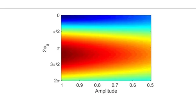
To find an optimum value for the phase amplitude faof the PM regarding a potential application, we
conducted simulations of the BB evolution. Figure11shows a result with the intensity of the central maximum ICMbeing the evaluation criterion. The simulations were conducted with PM parameters of D=10 μm and
kr=5 μm−1and with an electron energy of 300 keV. Figure11shows the value of ICMof a BB propagated Figure 10. Comparison of experimental (left) and simulated BBs (right) shows very good agreement for different effective propagation distances.
Figure 11. Simulated intensity of ICMof a BB with kr=5 μm−1and D=10 μm propagated 432 mm (0.86·zmax)after transmission
through the PM in dependence of the phase (fa)and amplitude modulation (Aa)of the generating PM. ICMis color coded from blue
(low intensity) to red (high intensity). The optimum PM induces a pure phase modulation of 2ja≈1.2π.
9
432 mm (0.86·zmaxafter transmission through the PM in dependence of the phase shift 2faand the amplitude
modulation 2Aainduced by the PM. The highest intensity (red) is reached for a pure phase shift of 1.2π and
decreases with both de- and increasing amount of phase shift as well as with increasing amplitude modulation. The simulations suggest that fa=2.3π of the PM implemented in the Hitachi HF-3300 is not ideal as it
differs from a phase shift of 1.2π. A more detailed analysis of the simulations show that the propagation distance at which the maximum value for ICMis obtained, decreases with increasing 2faabove 1.2π. Above this
propagation distance, the BB gets distorted which is in agreement with the experimental finding of the distorted appearance of the BB for larger propagation distances (figure8(c)). The effect of a focusing lens is neglected in the simulations and is responsible for the further increasing ICMfor higher effective propagation distances in the
experiment (figure9(c)) as it demagnifies the BB and thus increases the beam current density.
5. Potential applications of BB
We succeeded to generate BBs with an Å-sized central maximum in the sample plane of a transmission electron microscope. In addition, our experimental results agree very well with theory and with simulations.
Nevertheless, STEM imaging with the presented BBs is not beneficial compared to conventional STEM probes. Here we discuss the limitations and propose further optimization to be considered in order to exploit the beneficial characteristics of BBs and to be able to compete with existing conventional STEM probes. We finally present a range of techniques in which such optimized BBs could be applied.
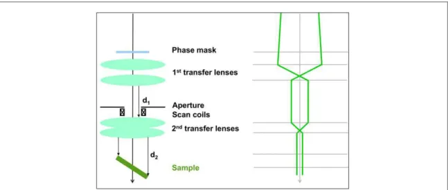
BBs develop in the Fresnel regime of a direct PM. As the electron optics of the condenser lens system of transmission electron microscopes is designed to create either an image or a diffraction pattern of a condenser aperture in the sample plane, they are not ideally suited for BB generation. Figure12shows a sketch of a potential lens setup with two transfer lens doublets. The PM with periodicity kris illuminated with an electron wave with a
very low convergence (plane wave) and the following transfer lens doublet demagnifies the PM by a factor of M1 which simultaneously decreases zmaxand increases kr. In the following free space with length d1, the BB can
evolve. Finally, the second transfer lens doublet further demagnifies the BB (M2) on the sample. Fresnel diffraction at the edge of the PM, as well as the outer rings of the BB can be blocked by an obstructing aperture shortly before the second transfer lens doublet without destroying the non-diffractive property in the necessary range of working distance (d2). Two pairs of scan coils located below the aperture allow to scan the beam over the
sample. If designed appropriately, the setup allows PMs with different properties (D, kr)as the physical
propagation distances d1and d2can be tuned to the necessary effective propagation distances by adjusting the
lens currents.
There are two main fields of potential applications for BBs: first, in imaging modes where a large focal depth is required. Large focal depths would be highly beneficial in scanning EM, where large differences in working distances (=d2)are very common. Focused imaging of samples located at different working distances would be
possible with BBs. In STEM conducted in a TEM, BBs are promising in tomography where high sample tilts are applied and a high DOF is necessary to image the whole sample area in focus [27].
As already stated above, the non-diffractive property of the electron beams comes at the expense of a reduced intensity in the central maximum. To keep the reduction of the signal-to-noise ratio at a tolerable value, the
Figure 12. Scheme of condenser lens system for BB generation with two transfer lens doublets demagnifying the BB resulting from the implemented phase mask on the sample.
number of rings should be chosen adequately. A value of nrings=5, which implies that roughly 20% of the
intensity is allocated in the central maximum, has already been successfully applied in light microscopy [22].
The second field of application are dose-dependent processes. The central maximum of the BB only represents a fraction of the total intensity in the beam which decreases the signal-to-noise ratio if the BB is used for imaging. However, the areal dose in the central maximum is tremendously larger than in the surrounding rings. If BBs are applied in dose-dependent processes such as lithography or electron-beam manipulation [28],
the surrounding rings only represent a small dose which could potentially be tolerated.
6. Conclusions
Direct PMs are well suited to generate quasi non-diffractive electron BBs for application in EM. The following conclusions can be drawn from our results obtained by experiment and simulation:
• We optimized the fabrication process of direct PMs by applying a lift-off process to create Pt apertures and custom circular scan routines for FIB milling of the necessary thickness profile. This leads to an enhanced homogeneity of the PM and to an improved quality of the generated electron beams.
• The electron-beam evolution of BBs can be analyzed in great detail by using the PM as specimen in a
transmission electron microscope. The experiments reveal, e.g. the quasi non-diffractive behavior, the Bessel-type beam shape and the oscillating increase of the intensity of the central maximum which is predicted by theory.
• The implementation of a PM in the condenser aperture allows the generation of BBs in the specimen plane and their control by the condenser lens system. A high demagnification of the PM in the order of 104is achieved in a Hitachi HF-3300.
• Simulations show good qualitative agreement with the experimental results and can be used to derive PM parameters for generation of optimum BBs.
• To find an optimum design of the PM, three parameters have to be considered: the diameter D, the Bessel frequency kr, and the phase amplitude faof the PM. While D should be chosen similar to conventional EM
apertures for high-resolution application, krmay be defined by the desired number of rings N from the
relation N=D·kr. Simulations show that 2fa=1.2 π leads to a BB with the highest intensity.
• We propose a four lens condenser system with which the application of BBs could be optimized and which would allow the beneficial application of BBs in, e.g. scanning electron microscopy.
Acknowledgments
Funding by Carl-Zeiss-Stiftung is acknowledged. We acknowledge support by Deutsche
Forschungsgemeinschaft and Open Access Publishing Fund of Karlsruhe Institute of Technology. S H thanks D Gerthsen for her ongoing support as well as E Müller and R Janzen for fruitful discussions. The ongoing support of Hitachi High Technologies Canada and Hitachi High Technologies, Naka, Japan was critical to enable study of BBs in the Hitachi HF-3300 at NRC-NANO. Discussions with Dr Yoshifumi Taniguchi were important to optimize the electron optics of the Hitachi HF-3300 for the purposes of this research.
ORCID iDs
Simon Hettler https://orcid.org/0000-0002-9102-7895
Lukas Grünewald https://orcid.org/0000-0002-5898-0713
References
[1] Uchida M and Tonomura A 2010 Generation of electron beams carrying orbital angular momentum Nature464 737–9
[2] Béché A, Juchtmans R and Verbeeck J 2017 Efficient creation of electron vortex beams for high resolution STEM imaging Ultramicroscopy178 12–9
[3] Béché A, Winkler R, Plank H, Hofer F and Verbeeck J 2016 Focused electron beam induced deposition as a tool to create electron vortices Micron 80 34–8
[4] Shiloh R, Lereah Y, Lilach Y and Arie A 2014 Sculpturing the electron wave function using nanoscale phase masks Ultramicroscopy144 26–31
11
[5] Verbeeck J, Béché A, Müller-Caspary K, Guzzinati G, Luong M A and Den Hertog M 2018 Demonstration of a 2×2 programmable phase plate for electrons Ultramicroscopy190 58–65
[6] Blackburn A M and Loudon J C 2014 Vortex beam production and contrast enhancement from a magnetic spiral phase plate Ultramicroscopy136 127–43
[7] Bliokh K Y et al 2017 Theory and applications of free-electron vortex states Phys. Rep.690 1–70
[8] McMorran B, Agrawal A, Anderson I A, Herzing A A, Lezec H J, McClelland J J and Unguris J 2011 Electron vortex beams with high quanta of orbital angular momentum Science331 192–5
[9] Pohl D, Schneider S, Rusz J and Rellinghaus B 2015 Electron vortex beams prepared by a spiral aperture with the goal to measure EMCD on ferromagnetic films via STEM Ultramicroscopy150 16–22
[10] Verbeeck J, Tian H and Schattschneider P 2010 Production and application of electron vortex beams Nature467 301–4
[11] Voloch-Bloch N, Lereah Y, Lilach Y, Gover A and Arie A 2013 Generation of electron airy beams Nature494 331–5
[12] Grillo V, Harris J, Gazzadi G C, Balboni R, Mafakheri E, Dennis M R, Frabboni S, Boyd R W and Karimi E 2016 Generation and application of Bessel beams in electron microscopy Ultramicroscopy166 48–60
[13] Grillo V, Karimi E, Gazzadi G C, Frabboni S, Dennis M R and Boyd R W 2014 Generation of nondiffracting electron Bessel beams Phys. Rev. X4 011013
[14] Shiloh R, Remez R, Lu P H, Jin L, Lereah Y, Tavabi A H, Dunin-Borkowski R E and Arie A 2018 Spherical aberration correction in a scanning transmission electron microscope using a sculpted thin film Ultramicroscopy189 46–53
[15] Durnin J 1987 Exact solutions for nondiffracting beams: I. The scalar theory J. Opt. Soc. Am. A4 651–4
[16] Nambu H, Noguchi Y, Saitoh K and Uchida M 2017 Nearly nondiffracting electron lattice beams generated by polygonal slits Microscopy 66 295–9
[17] Saitoh K, Hirakawa K, Nambu H, Tanaka N and Uchida M 2016 Generation of electron Bessel beams with nondiffractive spreading by a nanofabricated annular slit J. Phys. Soc. Japan85 043501
[18] Zheng C, Petersen T C, Kirmse H, Neumann W, Morgan M J and Etheridge J 2017 Axicon lens for electrons using a magnetic vortex: the efficient generation of a bessel beam Phys. Rev. Lett.119 174801
[19] D’Alfonso A J, Findlay S D, Oxley M P, Pennycook S J, van Benthem K and Allen L J 2007 Depth sectioning in scanning transmission electron microscopy based on core-loss spectroscopy Ultramicroscopy108 17–28
[20] Aoyama K, Takagi T, Hirase A and Miyazawa A 2008 STEM tomography for thick biological specimens Ultramicroscopy109 70–80
[21] Biskupek J, Leschner J, Walther P and Kaiser U 2010 Optimization of STEM tomography acquisition-a comparison of convergent beam and parallel beam STEM tomography Ultramicroscopy110 1231–7
[22] Fahrbach F O, Simon P and Rohrbach A 2010 Microscopy with self-reconstructing beams Nat. Photon.4 780–5
[23] Planchon T A, Gao L, Milkie D E, Davidson M W, Galbraith J A, Galbraith C G and Betzig E 2011 Rapid three-dimensional isotropic imaging of living cells using Bessel beam plane illumination Nat. Methods8 417–23
[24] Vasara A, Turunen J and Friberg A T 1989 Realization of general nondiffracting beams with computer-generated holograms J. Opt. Soc. Am A6 1748–54
[25] Durnin J, Miceli J J and Eberly J H 1987 Diffraction-free beams Phys. Rev. Lett.58 1499–501
[26] Bergen M, Malac M, McLeod R A, Hoyle D, Taniguchi Y, Yaguchi Y, Chen J and Yotsuji T 2013 Centralized instrument Control for a TEM laboratory Microsc. Microanal.19 1394–5
[27] Hayashida M and Malac M 2016 Practical electron tomography guide: recent progress and future opportunities Micron 91 49–74 [28] Susi T, Meyer J C and Kotakoski J 2017 Manipulating low-dimensional materials down to the level of single atoms with electron