Publisher’s version / Version de l'éditeur:
Optics Express, 18, 19, pp. 20251-20262, 2010-09-08
READ THESE TERMS AND CONDITIONS CAREFULLY BEFORE USING THIS WEBSITE. https://nrc-publications.canada.ca/eng/copyright
Vous avez des questions? Nous pouvons vous aider. Pour communiquer directement avec un auteur, consultez la première page de la revue dans laquelle son article a été publié afin de trouver ses coordonnées. Si vous n’arrivez Questions? Contact the NRC Publications Archive team at
PublicationsArchive-ArchivesPublications@nrc-cnrc.gc.ca. If you wish to email the authors directly, please see the first page of the publication for their contact information.
NRC Publications Archive
Archives des publications du CNRC
This publication could be one of several versions: author’s original, accepted manuscript or the publisher’s version. / La version de cette publication peut être l’une des suivantes : la version prépublication de l’auteur, la version acceptée du manuscrit ou la version de l’éditeur.
For the publisher’s version, please access the DOI link below./ Pour consulter la version de l’éditeur, utilisez le lien DOI ci-dessous.
https://doi.org/10.1364/OE.18.020251
Access and use of this website and the material on it are subject to the Terms and Conditions set forth at
Subwavelength grating periodic structures in silicon-on-insulator : A
new type of microphotonic waveguide
Bock, Przemek J.; Cheben, Pavel; Schmid, Jens H.; Lapointe, Jean; Delâge,
André; Janz, Siegfried; Aers, Geof C.; Xu, Dan-Xia; Densmore, Adam; Hall,
Trevor J.
https://publications-cnrc.canada.ca/fra/droits
L’accès à ce site Web et l’utilisation de son contenu sont assujettis aux conditions présentées dans le site LISEZ CES CONDITIONS ATTENTIVEMENT AVANT D’UTILISER CE SITE WEB.
NRC Publications Record / Notice d'Archives des publications de CNRC:
https://nrc-publications.canada.ca/eng/view/object/?id=32d4e095-aaa8-47f7-874a-d6ec05d1b9af https://publications-cnrc.canada.ca/fra/voir/objet/?id=32d4e095-aaa8-47f7-874a-d6ec05d1b9afSubwavelength grating periodic
structures in silicon-on-insulator:
a new type of microphotonic waveguide
Przemek J. Bock,1,2,* Pavel Cheben,1 Jens H. Schmid,1 Jean Lapointe,1 André Delâge,1 Siegfried Janz,1 Geof C. Aers,1 Dan-Xia Xu,1 Adam Densmore,1 and Trevor J. Hall2
1Institute for Microstructural Sciences, National Research Council Canada, Ottawa, Canada 2Centre for Research in Photonics, University of Ottawa, Ottawa, Canada
*przemek.bock@nrc.ca
Abstract: We report on the experimental demonstration and analysis of a
new waveguide principle using subwavelength gratings. Unlike other periodic waveguides such as line-defects in a 2D photonic crystal lattice, a subwavelength grating waveguide confines the light as a conventional index-guided structure and does not exhibit optically resonant behaviour. Subwavelength grating waveguides in silicon-on-insulator are fabricated with a single etch step and allow for flexible control of the effective refractive index of the waveguide core simply by lithographic patterning. Experimental measurements indicate a propagation loss as low as 2.1 dB/cm for subwavelength grating waveguides with negligible polarization and wavelength dependent loss, which compares favourably to conventional microphotonic silicon waveguides. The measured group index is nearly constant ng ~1.5 over a wavelength range exceeding the telecom C-band. ©2010 Optical Society of America
OCIS codes: (130.3120) Integrated optics devices; (050.1950) Diffraction gratings; (050.6624) Subwavelength structures.
References and links
1. F. P. Payne, and J. P. R. Lacey, “A theoretical analysis of scattering loss from planar optical waveguides,” Opt. Quantum Electron. 26(10), 977–986 (1994).
2. R. Pafchek, R. Tummidi, J. Li, M. A. Webster, E. Chen, and T. L. Koch, “Low-loss silicon-on-insulator shallow-ridge TE and TM waveguides formed using thermal oxidation,” Appl. Opt. 48(5), 958–963 (2009).
3. F. Grillot, L. Vivien, S. Laval, D. Pascal, and E. Cassan, “Size influence on the propagation loss induced by sidewall roughness in ultrasmall SOI waveguides,” IEEE Photon. Technol. Lett. 16(7), 1661–1663 (2004). 4. J. H. Schmid, A. Delâge, B. Lamontagne, J. Lapointe, S. Janz, P. Cheben, A. Densmore, P. Waldron, D.-X. Xu,
and K.-P. Yap, “Interference effect in scattering loss of high-index-contrast planar waveguides caused by boundary reflections,” Opt. Lett. 33(13), 1479–1481 (2008).
5. T. G. Nguyen, R. S. Tummidi, T. L. Koch, and A. Mitchell, “Lateral leakage of TM-like mode in thin-ridge Silicon-on-Insulator bent waveguides and ring resonators,” Opt. Express 18(7), 7243–7252 (2010). 6. P. Dumon, W. Bogaerts, V. Wiaux, J. Wouters, S. Beckx, J. Van Campenhout, D. Taillaert, B. Luyssaert, P.
Bienstman, D. Van Thourhout, and R. Baets, “Low-loss SOI photonic wires and ring resonators fabricated with deep UV lithography,” IEEE Photon. Technol. Lett. 16(5), 1328–1330 (2004).
7. Y. A. Vlasov, and S. J. McNab, “Losses in single-mode silicon-on-insulator strip waveguides and bends,” Opt. Express 12(8), 1622–1631 (2004).
8. M. Gnan, S. Thoms, D. S. Macintyre, R. M. De La Rue, and M. Sorel, “Fabrication of low-loss photonic wires in silicon-on-insulator using hydrogen silsesquioxane electron-beam resist,” Electron. Lett. 44(2), 115–116 (2008). 9. F. Xia, L. Sekaric, and Y. A. Vlasov, “Ultracompact optical buffers on a silicon chip,” Nat. Photonics 1(1), 65–
71 (2007).
10. J. Cardenas, C. B. Poitras, J. T. Robinson, K. Preston, L. Chen, and M. Lipson, “Low loss etchless silicon photonic waveguides,” Opt. Express 17(6), 4752–4757 (2009).
11. S. Fan, J. D. Joannopoulos, J. N. Winn, A. Devenyi, J. C. Chen, and R. D. Meade, “Guided and defect modes in periodic dielectric waveguides,” J. Opt. Soc. Am. B 12(7), 1267–1272 (1995).
12. S. Ha, A. A. Sukhorukov, D. A. Powell, I. V. Shadrivov, A. V. Lavrinenko, D. N. Chigrin, and Y. S. Kivshar, “Observation of Slow Light Tunneling in Coupled Periodic Waveguides,” in Frontiers in Optics, OSA Technical Digest (Optical Society of America, 2008), paper FWL3.
13. S. Ha, A. A. Sukhorukov, K. B. Dossou, L. C. Botten, A. V. Lavrinenko, D. N. Chigrin, and Y. S. Kivshar, “Dispersionless tunneling of slow light in antisymmetric photonic crystal couplers,” Opt. Express 16(2), 1104– 1114 (2008).
14. E. Dulkeith, S. J. McNab, and Y. A. Vlasov, “Mapping the optical properties of slab-type two-dimensional photonic crystal waveguides,” Phys. Rev. B 72(11), 115102 (2005).
15. E. Kuramochi, M. Notomi, S. Hughes, A. Shinya, T. Watanabe, and L. Ramunno, “Disorder-induced scattering loss of line-defect waveguides in photonic crystal slabs,” Phys. Rev. B 72(16), 161318 (2005).
16. L. O'Faolain, X. Yuan, D. McIntyre, S. Thoms, H. Chong, R. M. De La Rue, and T. F. Krauss, “Low-loss propagation in photonic crystal waveguides,” Electron. Lett. 42(25), 1454–1456 (2006).
17. Z. Weissman, and A. Hardy, “2-D mode tapering via tapered channel waveguide segmentation,” Electron. Lett. 28(16), 1514–1516 (1992).
18. P.-G. Luan, and K. D. Chang, “Transmission characteristics of finite periodic dielectric waveguides,” Opt. Express 14(8), 3263–3272 (2006).
19. M. M. Spühler, B. J. Offrein, G.-L. Bona, R. Germann, I. Massarek, and D. Erni, “A very short planar silica spot-size converter using a nonperiodic segmented waveguide,” J. Lightwave Technol. 16(9), 1680–1685 (1998). 20. M. H. Chou, M. A. Arbore, and M. M. Fejer, “Adiabatically tapered periodic segmentation of channel
waveguides for mode-size transformation and fundamental mode excitation,” Opt. Lett. 21(11), 794–796 (1996). 21. J. Teng, P. Dumon, W. Bogaerts, H. Zhang, X. Jian, M. Zhao, G. Morthier, and R. Baets, “Athermal
Silicon-on-insulator ring resonators by overlaying a polymer cladding on narrowed waveguides,” Opt. Express 17(17), 14627–14633 (2009).
22. C. Karnutsch, C. L. C. Smith, A. Graham, S. Tomljenovic-Hanic, R. Mcphedran, B. J. Eggleton, L. O’Faolain, T. F. Krauss, S. S. Xiao, and N. A. Mortensen, “Temperature stabilization of optofluidic photonic crystal cavities,” Appl. Phys. Lett. 94(23), 231114 (2009).
23. S. M. Rytov, “Electromagnetic properties of a finely stratified medium,” Sov. Phys. JETP 2, 466–475 (1956). 24. P. Lalanne, and J.-P. Hugonin, “High-order effective-medium theory of subwavelength gratings in classical
mounting: application to volume holograms,” J. Opt. Soc. Am. A 15(7), 1843–1851 (1998).
25. H. Kikuta, H. Toyota, and W. Yu, “Optical elements with subwavelength structured surfaces,” Opt. Rev. 10(2), 63–73 (2003).
26. C. F. R. Mateus, M. C. Y. Huang, L. Chen, C. J. Chang-Hasnain, and Y. Suzuki, “Broad-band mirror (1.12–1.62 m) using a subwavelength grating,” IEEE Photon. Technol. Lett. 16(7), 1676–1678 (2004).
27. P. Cheben, D.-X. Xu, S. Janz, and A. Densmore, “Subwavelength waveguide grating for mode conversion and light coupling in integrated optics,” Opt. Express 14(11), 4695–4702 (2006).
28. P. Cheben, S. Janz, D.-X. Xu, B. Lamontagne, A. Delâge, and S. Tanev, “Highly efficient broad-band waveguide grating coupler with a sub-wavelength grating mirror,” in Frontiers in planar lightwave circuit technology, S. Janz et al., eds. (Springer, 2006), 235–243.
29. R. Halir, P. Cheben, S. Janz, D.-X. Xu, I. Molina-Fernández, and J. G. Wangüemert-Pérez, “Waveguide grating coupler with subwavelength microstructures,” Opt. Lett. 34(9), 1408–1410 (2009).
30. J. H. Schmid, P. Cheben, S. Janz, J. Lapointe, E. Post, and D.-X. Xu, “Gradient-index antireflective subwavelength structures for planar waveguide facets,” Opt. Lett. 32(13), 1794–1796 (2007).
31. J. H. Schmid, P. Cheben, S. Janz, J. Lapointe, E. Post, A. Delâge, A. Densmore, B. Lamontagne, P. Waldron and D.-X. Xu, “Subwavelength grating structures in silicon-on-insulator waveguides,” Advances in Optical Technologies: Special Issue on Silicon Photonics, 2008, Article ID 685489, doi:10.1155/2008/685489. 32. M. Hochberg, T. Baehr-Jones, C. Walker, J. Witzens, L. C. Gunn, and A. Scherer, “Segmented waveguides in
thin silicon-on-insulator,” J. Opt. Soc. Am. B 22(7), 1493–1497 (2005).
33. P. J. Bock, P. Cheben, J. H. Schmid, J. Lapointe, A. Delâge, D.-X. Xu, S. Janz, A. Densmore, and T. J. Hall, “Subwavelength grating crossings for silicon wire waveguides,” Opt. Express 18(15), 16146–16155 (2010). 34. P. Cheben, P. J. Bock, J. H. Schmid, J. Lapointe, S. Janz, D.-X. Xu, A. Densmore, A. Delâge, B. Lamontagne,
and T. J. Hall, “Refractive index engineering with subwavelength gratings for efficient microphotonic couplers and planar waveguide multiplexers,” Opt. Lett. 35(15), 2526–2528 (2010).
35. M. Kuznetsov, and H. A. Haus, “Radiation loss in dielectric waveguide structures by the volume current method,” IEEE J. Quantum Electron. 19(10), 1505–1514 (1983).
36. D. Ortega, J. M. Aldariz, J. M. Arnold, and J. S. Aitchison, “Analysis of quasi-modes in periodic segmented waveguides,” J. Lightwave Technol. 17(2), 369–375 (1999).
37. http://ab-initio.mit.edu/wiki/index.php/MIT_Photonic_Bands.
38. Y. A. Vlasov, M. O’Boyle, H. F. Hamann, and S. J. McNab, “Active control of slow light on a chip with photonic crystal waveguides,” Nature 438(7064), 65–69 (2005).
1. Introduction
Light can be confined in a dielectric waveguide by index-guiding or by exciting defect states in a periodic lattice. A conventional planar waveguide confines the light in a core, which has a higher refractive index than the surrounding cladding material. However, the high refractive index contrast of silicon waveguides results in large scattering at the core-cladding boundary imperfections [1]. High refractive index contrast ridge waveguides minimize this effect with a
larger core size at the expense of an increased bending radius [2]. For channel waveguides, scattering efficiency can be reduced by using waveguides with a core area that is small enough to delocalize the waveguide mode, such that the field intensity at the core-cladding boundary is diminished [3] or by making use of an inherent interference effect of the scattered radiation [4,5]. Large dependence of propagation loss on waveguide geometry [6], wavelength and polarization [7] has been reported for silicon wire waveguides. Such dramatic changes of loss in silicon wire waveguides are a significant obstacle in building practical microphotonic circuits. Low loss of 1 dB/cm [8] to 1.7 dB/cm [9] has been achieved for transverse electric (TE) polarization. However, square core cross-sections are intentionally avoided to reduce the vertical sidewall height, resulting in optimal TE performance at typical waveguides dimensions of 500 nm × 200 nm. The penalty for this optimized waveguide TE performance is that a confined transverse magnetic (TM) mode may no longer be supported by the waveguide (depending on the cladding material used) [5]. Since sidewall imperfections originate from the etching process, propagation loss can be reduced by using an etchless process based on selective oxidation [10], although such waveguides support only TE polarization and insertion loss is significant.
Periodic photonic lattices have also been investigated for waveguiding, but the efforts have almost exclusively focused on photonic crystals with d ~λ/(2neff) that have a band gap at
the operational frequency range. In such structures, a waveguide is created by introducing a line-defect in the periodic lattice that creates defect states localized within the lattice’s photonic band gap. Waveguides made of periodic dielectric rods have been theoretically considered [11], including first implementations in the fast light regime [12,13]. Typical line defect photonic crystal waveguides have propagation losses ranging from 8 dB/cm to 4.1 dB/cm [14–16]. However, these waveguides exhibit wavelength and polarization dependent losses.
In this paper, a new waveguide principle based on the formation of a subwavelength grating (SWG) in a waveguide core is proposed and demonstrated experimentally. In contrast to waveguides based on line-defects in 2D photonic crystal lattices, the light is confined in a SWG waveguide core covered with a cladding material of a lower refractive index, as in conventional index-guided structures. The core is a composite medium formed by periodically interlacing silicon segments with a material of a lower refractive index at the subwavelength scale.
Several types of segmented waveguides have been previously studied numerically [17,18] and also experimentally [19,20]. The latter have been proposed as long-period-grating tapers with a segmentation pitch of Λ >> λ/(2neff), where λ is the wavelength in vacuum and neff is
effective index, for mode size transformation in low-index-contrast waveguides such as those made in a silica-on-silicon material platform. However, application of such structures in high-index-contrast waveguides is hindered by the reflection and the diffraction losses incurred at the boundaries of the different segments.
The long-period segmented waveguides do not support a (theoretically) lossless mode and the light coupling to radiation modes limits applications of such structures to short propagation lengths and small refractive index discontinuities. Our subwavelength grating waveguide is unique in that the structure supports a true lossless mode. By modifying the pitch, width and duty cycle of the subwavelength grating, the effective index of the medium can be engineered locally. This technique provides a means to tailor the effective index, mode profile and dispersion of the subwavelength grating waveguide. In our study, we used silicon segments with SU-8 cladding material; however any materials can be interlaced for specific applications. For example, athermal waveguides [21,22] can be designed by interlacing materials with opposite polarity thermo-optic coefficients, while waveguide modulators or lasers may be implemented by making or interlacing waveguide core segments with a nonlinear optical material. This freedom in waveguide design suggests that subwavelength grating waveguides can be used in a broad range of applications.
2. Subwavelength grating principle and simulation
Subwavelength gratings can be used to create artificial media engineered at a microscopic scale to achieve a desired macroscopic behaviour. For the silicon-on-insulator (SOI) material platform, a subwavelength grating can be created by the combination of single crystal silicon with silica (SiO2) or other low index materials such as SU-8 polymer. These periodic
structures frustrate diffraction and behave like a homogeneous medium (metamaterial) provided the periodicity does not satisfy a Bragg condition for coupling to other confined or radiative modes [23,24].
Subwavelength gratings have been extensively used for antireflective coatings on bulk optical surfaces [25]. Originally implemented as planar mirrors [26], subwavelength gratings have been used as efficient fibre-chip couplers [27], off-plane fibre couplers [28,29], antireflective gradient index structures and interference mirrors [30,31]. Subwavelength gratings were originally proposed as silicon waveguide cores [27] and as a composite waveguide cladding [32]. Recently, subwavelength gratings have been experimentally demonstrated as efficient crossings [33] and adiabatic mode transformers and fibre-chip couplers [34].
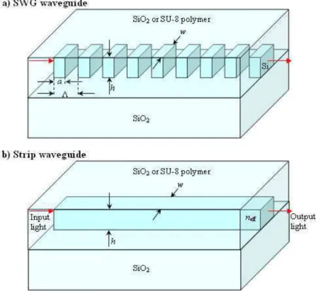
Fig. 1. Schematic of a) a SWG waveguide and b) an equivalent strip waveguide. An effective material refractive index neff of the equivalent wire waveguide is determined by spatial
averaging of refractive indexes of the waveguide core (Si) and the cladding (SiO2, SU-8, air,
etc.) materials at a subwavelength scale. The resulting effective index can be controlled by lithography (changing grating duty ratio a/Λ, width w, etc.).
In a subwavelength grating waveguide with a core consisting of a periodic arrangement of silicon and silica segments, light excites a Bloch mode, which can propagate through the segmented waveguide theoretically without losses caused by diffraction into radiative or cladding modes. A schematic of a SWG waveguide is shown in Fig. 1(a), including an equivalent wire waveguide with an engineered core refractive index [Fig. 1(b)].
In our nominal SWG waveguide, the grating period, duty cycle and segment dimensions are chosen to avoid the formation of standing waves due to Bragg scattering and the opening of a band gap near λ = 1550 nm wavelength. According to this criteria and using finite-difference time-domain and MIT photonic bands (frequency domain) calculations, the following structural parameters were chosen: grating pitch Λ = 300 nm, segment width w = 300 nm and segment length a = 150 nm. Note that the grating pitch is less than a half of the effective wavelength of the waveguide mode λeff = λ/2neff. For these parameters, the mode
delocalization from the core yields a reduced field intensity at the core-cladding boundary, thereby reducing scattering loss by the sidewall imperfections. The mode delocalization is also evident in Fig. 2, showing an increased effective mode size for the SWG waveguide compared to a conventional wire waveguide of the same width. The chosen grating parameters minimize wavelength resonances due to diffraction effects, as it is evident in the calculated dispersion diagram (Fig. 3). Notice that the subwavelength grating waveguide at λ = 1550 nm is far outside the photonic bandgap region.
It is know that waveguide scattering loss is determined by the amplitude of the current source (the defect volume element interacting with the local electric field [35]) as well as the cumulative (interference) effect of the spatial distribution of the scattering sources. A subwavelength grating waveguide effectively minimizes the source amplitude by delocalizing the mode, thereby decreasing electric field interaction with the volume defect. Furthermore, the gaps in-between the high-index segments shorten the mode interaction length with the sidewalls.
Three-dimensional (3D) finite-difference time-domain (FDTD) simulation is used to estimate the mode profile of a SWG waveguide and how it compares to the mode profile of a wire waveguide. All simulations are done on a layout size of x × y × z = 3 × 3.26 × 10 m3 having a mesh resolution of x × y × z = 10 × 10 × 10 nm3. Material refractive indices used are nSi = 3.476 for the waveguide core, nSiO2 = 1.444 for the waveguide lower cladding
(bottom oxide, BOX), and nSiO2 = 1.444 or nSU8 = 1.577 for the waveguide upper cladding, as
either SiO2 or SU-8 upper cladding is used in simulations. The simulation time step is 1.67 ×
10−17
s according to the Courant criterion t ≤ 1/(c(1/( x)2 + 1/( y)2 + 1/( z)2)½), where c is the speed of light in vacuum. The simulated structure consists of a 10 m long SWG straight waveguide with Λ = 300 nm, w = 300 nm and a = 150 nm. The Si wire (width 300 nm) waveguide mode is used to excite the SWG waveguide Bloch mode at λ = 1550 nm for TE polarization. The mode profile of the SWG is recorded at the center (x-y plane) of every 4th grating segment. To estimate the steady-state mode profile of the SWG waveguide (in the center of a grating segment), the overlap integral of each recorded mode profile is calculated with the mode profile 4 grating segments back. Steady-state behaviour is assumed when this mode overlap integral is constant and approaches unity as shown in Fig. 2(a).
We estimate the overlap of the mode in the 300 nm wide SWG waveguide with a delocalized mode of a conventional wire waveguide with a width as small as 160 nm. Specifically, the overlap between these two modes is up to 90%, as it is shown in Fig. 2(b). It is also useful to consider the confinement factor Г, i.e. the fraction of the modal intensity confined within the waveguide core. Using the SWG mode profile, the overlap integral with a wire waveguide of varying widths (160 nm – 300 nm) was calculated to assess the SWG mode confinement [Fig. 2(b)]. For a Si-wire width of 160 nm the confinement factor is Г < 5%, whereas for a wire width of 300 nm, Г = 48%. Figure 2(b) shows that the SWG mode profile (w = 300 nm, SiO2 upper cladding) has only a 56% overlap with a 300 nm wide wire
waveguide. However, the same SWG waveguide mode has a ~90% overlap with a mode of 160 nm wide wire waveguide indicating the SWG mode is significantly delocalized, i.e. comparably delocalized to a mode of the 160 nm wide wire waveguide, and indeed is less confined that the mode in a 300 nm wide Si-wire.
Fig. 2. a) Calculated mode overlap integral as a function of mode profile position (z-coordinate). b) Overlap integral of the steady-state SWG mode profile with a wire waveguide of varying widths (160 nm – 300 nm). c) Mode profile of a wire waveguide (w = 300 nm, SiO2
upper cladding). d) Mode profile of a SWG waveguide (w = 300 nm, SiO2 upper cladding) at
the center of a Si segment (x-y plane). e) Field propagating along the subwavelength grating, excited by the wire waveguide mode at λ = 1550 nm, for quasi-TE polarization.
Mode profiles for a 300 nm wide wire waveguide and SWG waveguide are shown in Figs. 2(c) and 2(d) respectively, while the propagating field along the grating is shown in Fig. 2(e), for a SWG waveguide with SiO2 upper cladding. Using the approximation of mode
size from earlier work in long-period waveguide gratings [36], the refractive index contrast of a periodic waveguide neff is equivalent to an effective refractive index contrast of a uniform waveguide by neff ~η nuniform, where η is the duty cycle (50% in our nominal design). Assuming silicon segments and silica upper cladding, neff = η nuniform ~1 resulting in a 300 nm wide waveguide with nclad = 1.444 and ncore = 2.46. Alternatively, when SU-8 is used as
the upper cladding, nclad = 1.577 and ncore = 2.52. In either case, such an effective uniform
agreement with the approximation above. These results also suggest that because the mode is delocalized from the core, the scattering loss due to sidewall fabrication imperfections is reduced in SWG waveguides.
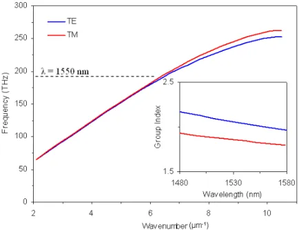
The SWG waveguide mode was also calculated using the MIT photonic bands (MPB) frequency-domain software [37], yielding good agreement with the FDTD simulations above. Furthermore, the group index of the nominal SWG waveguide was calculated using MPB with a layout size of x × y × z = 2 × 2 × 0.3 m3 having a mesh resolution of x × y × z = 20 × 20 × 20 nm3. The SU-8 upper cladding was chosen, as in our fabricated structures (see Section 3). In Fig. 3 the dispersion relation for the TE and TM modes of the SWG waveguide is shown, which exhibits the expected behaviour for a periodic waveguide, namely a flattening of the dispersion with increasing wavenumber β as the Bragg condition is approached. Due to the subwavelength nature of the grating, the operating frequency is well below this flat dispersion region, as shown in the Fig. 3. The group velocity of the propagating Bloch mode is given by the slope of the dispersion curve. The group index ng of the TE and TM modes of the SWG waveguide is shown in the inset of Fig. 3 as a function of wavelength. The group index varies in the range 2.2 – 2.0 for the TE and 2.0 – 1.8 for the TM modes over the wavelength range of λ = 1480 nm – 1580 nm. The calculated group index is close to the calculated effective index of the waveguide mode, confirming the absence of slow-light or resonant effects of the grating on the light propagation.
Fig. 3. a) Calculated dispersion diagram of a SWG waveguide consisting of 150 nm long Si segments separated by 150 nm long gaps filled with SU-8 polymer (nSU-8 = 1.577). Lower
cladding is silicon dioxide (nSiO2 = 1.444) and upper cladding is SU-8. Inset shows the group
index of the TE and TM modes for a wavelength range of λ = 1480 nm – 1580 nm.
3. Design and fabrication
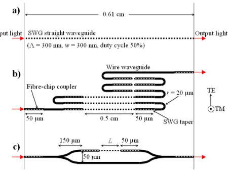
Subwavelength grating straight waveguides are fabricated with a length of 0.61 cm (equal to the chip length) as shown in Fig. 4(a). To estimate propagation loss, test structures are also fabricated with SWG straight waveguide sections of 0.5 cm, 1.5 cm and 3.0 cm in length [Fig. 4(b)]. In these test structures, silicon wire waveguides (450 × 260 nm2) are coupled to SWG straight waveguides using the 50 µm long adiabatic transformer shown in Fig. 5(c). The subsequent SWG section is 0.5 cm long with a constant pitch (Λ = 300 nm), width (w = 300 nm) and duty cycle (50%). SWG waveguides with 400 nm pitch were also included. An
identical adiabatic transformer section is used for the transition back to a wire waveguide. Wire waveguide U-bends of radius 20 µm are used in the test structure to fit multiple 0.5 cm long SWG straight waveguides on the chip, as indicated in Fig. 4(b), which shows an example of three 0.5 cm straight SWG sections. Test structures having varying SWG straight waveguide lengths all have identical wire lengths, number of bends, adiabatic transformers and fibre-chip couplers. Therefore the cumulative loss due to these elements is identical for each test structure, and will not affect the SWG loss measurement.
To estimate the group index of a SWG straight waveguide a Mach-Zehnder interferometer (MZI) is fabricated, where the reference arm is comprised of a wire waveguide (450 × 260 nm2), while the signal arm is comprised of a 50 µm SWG taper followed by a SWG (Λ = 300 nm, w = 300 nm, duty cycle 50%) with length L = 1000 µm, and an identical SWG taper to transition back to wire waveguide [Fig. 4(c) and Fig. 5(d)]. The MZI uses a 50:50 y-splitter implemented with two 150-µm-long and 25-µm-wide s-bends.
Fig. 4. a) Schematic of the test structure implemented for measuring the spectral response of a SWG straight waveguide with a length of 0.61 cm (equal to the chip length). b) Schematic of the test structure implemented for measuring propagation loss of a SWG straight waveguide. Wire waveguides (450 × 260 nm2) are transformed to the SWG straight waveguide using a 50
µm long taper with bridging segments, followed by a 0.5 cm long SWG with a constant pitch (Λ = 300 nm), width (w = 300 nm) and duty cycle (50%). An identical taper is used for the transition back to a wire waveguide and a 180° wire waveguide bend (radius of 20 µm) is used in the test structure to fit multiple 0.5 cm long SWG straight waveguides on the chip. The specific schematic shown in (b) has three SWG sections with a total length of 1.5 cm. c) Schematic of the Mach-Zehnder interferometer (MZI) which was used to estimate the group index of a SWG straight waveguide. Mach-Zehnder interferometer reference arm is a wire waveguide (450 × 260 nm2), while the signal arm is comprised of a 50 µm SWG taper
followed by a SWG waveguide (Λ = 300 nm and 400 nm, w = 300 nm, duty cycle 50%, length
L = 1000 µm) and a SWG taper to transition back to wire waveguide.
Structures were fabricated using commercially available SOI substrates with a 0.26 µm thick silicon layer and 2 µm thick buried oxide (BOX). Electron beam lithography was used to define the waveguide layout in high contrast hydrogen silsesquioxane resist, which formed SiO2 upon electron beam exposure. We used inductively coupled plasma reactive ion etching
a 2 µm thick polymer (SU-8, n ~1.577 at λ = 1.55 µm), then cleaved into separate chips and facets polished.
Figure 5 shows scanning electron microscope (SEM) images of fabricated structures including a SWG straight waveguide [Fig. 5(a)], detail of the grating segments [Fig. 5(b)], the first 15 µm of the 50 µm long SWG taper [Fig. 5(c)] and an optical microscope image of a MZI with SEM image detail of the signal arm (SWG straight waveguide) and reference arm (wire waveguide). From the SEM images it was determined that a fabrication bias of 50 nm was present. Therefore the actual dimensions of the SWG are Λ = 300 nm and w = 250 nm with a duty cycle of 33%. Actual wire waveguide width is 400 nm.
Fig. 5. Scanning electron microscope (SEM) images of fabricated structures including: a) SWG straight waveguide with Λ = 300 nm, w = 250 nm and a duty cycle of 33%. b) Detail of two SWG segments. c) The first 13 µm of the 50 µm long SWG taper. d) Optical microscope image of a MZI (LSWG = 100 m) with SEM image detail of the SWG arm and the reference arm (wire waveguide). Interferometric measurements (Fig. 7) were done with a MZI with a 1000 µm long SWG waveguide.
4. Experimental results
A tuneable external cavity semiconductor laser was used to measure the straight SWG waveguide transmission spectra over a wavelength range λ = 1480 nm – 1580 nm [Fig. 6(a)]. To measure the propagation loss, a broadband (3 dB bandwidth of λ = 1530 nm - 1560 nm) amplified spontaneous emission (ASE) source is used. To couple the light into the chip, a lensed fibre resulting in a Gaussian beam waist of ~2 µm (at the chip facet) is used with a SWG fibre-chip coupler [34]. Light is coupled out of the chip using another SWG coupler and subsequently focused by a microscope objective lens onto an InGaAs photodetector.
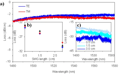
Propagation loss is estimated by measuring the transmitted power through the loss test structures of Fig. 4(b), with multiple repeats of SWG straight waveguides of lengths 0.5 cm, 1.5 cm and 3.0 cm. Loss is determined from the slope of a linear fit of transmitted power vs. SWG waveguide length. The transmission spectrum of the SWG straight waveguide is normalized to these measurements. Figure 6(a) shows the measured wavelength dependent propagation loss, while Fig. 6(b) indicates the measured loss using the ASE source. For our best SWG waveguides, the propagation loss is 2.1 dB/cm for TE polarization, whereas typical SWG waveguide loss measured on different test structures is 2.6 dB/cm. The PDL is less than 0.5 dB for the wavelength range shown. It is remarkable that such low loss is achieved for light propagating over a 1 cm distance through more than 33,000 boundaries between high- and low-refractive-index segments having an index contrast of n ~1.9. While this finding is consistent with Bloch mode theory, we also believe that this low loss is a direct consequence of the mode delocalization from the composite core with a corresponding decrease in light scattering at fabrication sidewalls imperfections, as found with the FDTD simulation mode profiles.
To confirm the loss measurements obtained with the ASE source, we repeated the same measurements on the loss test structures using the tuneable external cavity semiconductor laser. The loss values obtained using the single wavelength source fluctuated randomly from one wavelength to another, due to Fabry-Pérot cavity effects arising from the different elements of the test structure (wires, bends, taper and couplers). However, the propagation loss estimate of < 3.0 dB/cm in the C-band (λ = 1530 −1560 nm) is consistent with the typical wavelength averaged value of 2.6 dB/cm obtained using the ASE source.
The efficiency of the adiabatic transformer is approximately 0.5 dB [33]. Low overall transmission of loss test structures is the result of a rather complex layout [Fig. 4(b)], namely multiple wire-to-SWG mode transformers, Si wire waveguide segments, fibre-to-chip and chip-to-lens coupling interfaces, multiple U-bends, comparatively low input power level of our ASE source and the SWG waveguide loss itself. This layout was chosen to make certain that each test structure with different SWG waveguide length is continued with an identical wire waveguide length and contains the same number of bends and SWG couplers, since changing those parameters for SWG waveguides of different lengths could be misinterpreted as SWG loss, as we discussed in Section 3.
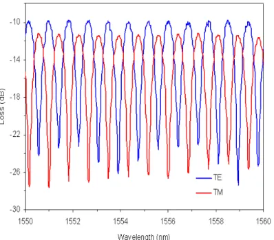
Fig. 6. a) Transmission spectra of a 0.61 cm long SWG straight waveguide measured for TE (blue) and TM (red) polarizations. b) Loss for meander test structures [Fig. 4(b)] with 0.5 cm, 1.5 cm and 3.0 cm long SWG waveguides of Λ = 400 nm, measured using an ASE broadband source. c) SWG waveguide transmission spectra (TE polarization).
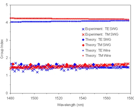
The group index of a SWG straight waveguide is measured interferometrically for a wavelength range of λ = 1480 nm – 1580 nm using a tuneable external cavity semiconductor laser. Group index is calculated using ngSWG = λminλmax/[2L(λmin - λmax)] + ngwire, where λmin and
λmax are the wavelengths at the minimum and maximum intensities of the interference fringes, L = 1000 µm is the length of the SWG straight waveguide and ngwire is the group index of the
reference wire waveguide [38]. Reference wire waveguide group index is estimated using a mode solver (Optiwave Corp.) to calculate the effective index of a 400 × 260 nm2 waveguide with silicon core and SU-8 cladding on a silica substrate for λ = 1480 nm – 1580 nm. The wire waveguide group index is found to be nearly constant across the wavelength range considered, with values of ngTE ~4.1 and ngTM ~4.2. Figure 7 shows the MZI spectral
transmittance for λ = 1550 nm – 1560 nm for TE and TM polarizations. Based on these measurements the calculated group index of a SWG waveguide is presented in Fig. 8 and is compared to the theoretically calculated (MPB [37]) group index for a periodic waveguide with the dimensions as measured by SEM, i.e. 33% duty cycle. Note that simulation results shown in Fig. 3 inset were obtained for our nominal SWG waveguide design with 50% duty cycle. The agreement between experiment and theory is excellent (Fig. 8), indicating a low and almost constant group index of ng ~1.5 over the measured wavelength range. Nearly
constant group index also indicates that SWG waveguides are potentially useful for high bit-rate processing as well as nonlinear optics applications.
Fig. 7. MZI spectral transmittance. MZI with a Si wire waveguide reference arm and a 1000 µm long SWG waveguide signal arm, for TE (blue) and TM (red) polarizations.
Fig. 8. The calculated and measured group index for a SWG waveguide. The group index of the reference wire waveguide for TE (blue circle) and TM (red circle) polarizations is estimated with a mode solver (Optiwave Corp.) by calculating the effective index of a 400 × 260 nm2 waveguide with silicon core, SU-8 upper cladding and SiO
2 bottom cladding. The
calculated group indexes for both the SWG waveguide and a photonic wire channel waveguide are shown for comparison.
5. Conclusion
We report on the theory and the experimental demonstration of a new waveguide principle based on subwavelength gratings. Measured propagation loss for our subwavelength grating waveguides is as low as 2.1 dB/cm and PDL is negligible, which compares favorably with other microphotonic waveguides. A theoretical analysis confirms that for comparable roughness, a SWG wire waveguide can be designed with a lower loss than conventional photonic wire waveguides, as the mode is delocalized and the interaction length with the sidewalls is reduced. If both polarizations are considered, the average loss for TE and TM of our SWG waveguide is one of the lowest yet reported for microphotonic waveguides. Measured group index of the SWG waveguide is in good agreement with the calculated values. An important advantage of SWG waveguides is that they allow for flexible control of the optical properties of the composite waveguide core, including its refractive index, mode size, thermal properties, and dispersion by combining the constituent materials at a subwavelength scale, simply by lithographic patterning. These results suggest that SWG waveguides can be important building blocks in future photonic devices.