Publisher’s version / Version de l'éditeur:
Information Photonics (IP), 2011 ICO International Conference on, 2011-05-20
READ THESE TERMS AND CONDITIONS CAREFULLY BEFORE USING THIS WEBSITE. https://nrc-publications.canada.ca/eng/copyright
Vous avez des questions? Nous pouvons vous aider. Pour communiquer directement avec un auteur, consultez la
première page de la revue dans laquelle son article a été publié afin de trouver ses coordonnées. Si vous n’arrivez pas à les repérer, communiquez avec nous à [email protected].
Questions? Contact the NRC Publications Archive team at
[email protected]. If you wish to email the authors directly, please see the first page of the publication for their contact information.
NRC Publications Archive
Archives des publications du CNRC
This publication could be one of several versions: author’s original, accepted manuscript or the publisher’s version. / La version de cette publication peut être l’une des suivantes : la version prépublication de l’auteur, la version acceptée du manuscrit ou la version de l’éditeur.
For the publisher’s version, please access the DOI link below./ Pour consulter la version de l’éditeur, utilisez le lien DOI ci-dessous.
https://doi.org/10.1109/ICO-IP.2011.5953765
Access and use of this website and the material on it are subject to the Terms and Conditions set forth at
Fast light-emitting silicon-germanium nanostructures for optical
interconnects
Lockwood, D. J.
https://publications-cnrc.canada.ca/fra/droits
L’accès à ce site Web et l’utilisation de son contenu sont assujettis aux conditions présentées dans le site LISEZ CES CONDITIONS ATTENTIVEMENT AVANT D’UTILISER CE SITE WEB.
NRC Publications Record / Notice d'Archives des publications de CNRC:
https://nrc-publications.canada.ca/eng/view/object/?id=ab1c6889-d1ed-41e4-8249-8cb71ed183fb https://publications-cnrc.canada.ca/fra/voir/objet/?id=ab1c6889-d1ed-41e4-8249-8cb71ed183fbFast Light-Emitting Silicon-Germanium
Nanostructures for Optical Interconnects
D. J. Lockwood
Institute for Microstructural Sciences National Research Council Ottawa, Ontario K1A 0R6, Canada
Abstract-Epitaxially-grown Si/SiGe quantum dot complexes
produce efficient photoluminescence and electroluminescence in the desired spectral range of 1.3-1.6 µm. The latest progress in our understanding of the physics of carrier recombination in Si/SiGe nanostructures is reviewed, and a new route toward CMOS compatible light emitters is proposed.
I. INTRODUCTION
Optical interconnects in the form of fiber optics have been used for many years in different long-distance communication applications. With the microprocessor clock speed approaching 10 Gbps, optical interconnects are now being considered for on-chip interconnects as an alternative to metal wires with their unavoidable RC delay, significant signal degradation, high power dissipation, and electromagnetic interference [1]. Two major avenues toward optical interconnects on a chip include a hybrid approach with densely packaged III-V optoelectronic components [2, 3] and the all-group-IV approach (mainly Si, Ge and SiGe), where all the major components, e.g., light emitters, modulators, waveguides and photodetectors, are monolithically integrated into the CMOS environment [1–3]. For several decades, efforts on obtaining light emission from group-IV semiconductors have been mainly focused on Si/Ge nanostructures (NSs) [2, 4]. However, no approach has so far been applied commercially. Reasons for this include the lack of compatibility with conventional CMOS technology, the long carrier radiative lifetime in Si-based NSs, and, especially in the case of near-infrared emitters, the significant thermal quenching of the luminescence quantum efficiency [4].
By the 1990s, a different form of SiGe NS, namely the three-dimensional (3D) self-assembled system produced by the Stranski-Krastanov growth mode in lattice mismatched materials, had been demonstrated [5]. It has been shown that dislocation-free SiGe growth can be achieved using a higher temperature (!600 oC), and that the non-planar geometry is mainly responsible for the significant increase of the SiGe critical layer thickness [5]. Compared to two-dimensional (2D) Si/SiGe NSs, the PL and electroluminescence (EL) quantum efficiency in 3D Si/SiGe NSs is higher (up to ~1%), especially for T > 50 K [6]. Despite many successful demonstrations of PL and EL in the spectral range of 1.3–1.6 µm, which is important for optical fiber communications, the proposed further development of 3D Si/SiGe based light emitters was discouraged by several studies indicating a type II energy band alignment at Si/SiGe heterointerfaces [6], where the spatial
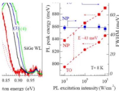
Figure 1. (a) Normalized PL spectra in CVD grown Si/SiGe 3D NSs showing the PL spectral shift to higher photon energy under increasing excitation intensity. Each spectrum can be fitted with two (NP and TO) Gaussian spectral
bands, as shown, for example, by the dashed lines under trace (1). (b) Summary of PL spectra changes as a function of excitation intensity.
separation of electrons (located in Si) and holes (localized in SiGe) was thought to make carrier radiative recombination very inefficient. Later, it was also shown that 3D Si/SiGe NSs exhibit an extremely long (~10-2 s) luminescence lifetime [6], which is ~106 times longer than in III-V semiconductors and their NSs. Thus, according to that analysis, 3D Si/SiGe NSs cannot be used to achieve efficient and commercially valuable light emitting devices. Here, we show that despite these facts it is still possible to obtain conditions favorable for efficient carrier radiative recombination in SiGe NSs.
II. LIGHT-EMITTING PROPERTIES
The PL spectra in 3D Si/SiGe NSs, which is similar to that in III-V quantum wells with type II energy band alignment, exhibit a blue shift as the excitation intensity increases [6]. This effect is found in both molecular bean epitaxy (MBE) and chemical vapor deposition (CVD) grown samples. Figure 1 shows PL spectra in a CVD grown sample measured under different excitation intensities. At the lowest excitation intensity used (0.1 W/cm2), the PL peaks at ~0.8 eV. With increasing excitation intensity, a continuous almost-parallel PL blue shift of 30–40 meV per decade of excitation intensity increase is observed. At an excitation intensity of 10 W/cm2, the PL peak reaches ~0.92 eV. Under photo-excitation of 1–10 kW/cm2, the low energy part of the PL spectrum does not shift further, while the high energy part continues shifting towards higher energy. A modified Arrhenius plot of the normalized integrated PL intensity as a function of temperature for the different excitation intensities can be fitted with two thermal
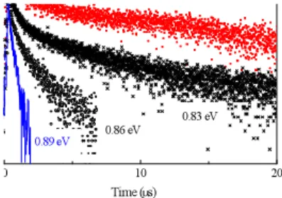
Figure 2. Low temperature PL dynamics for a CVD grown sample measured at the indicated photon energies using a ~6 ns excitation pulse.
Figure 3. Schematic of the Si/SiGe cluster multilayer energy band diagram with different electronic transitions labeled 1–5.
quenching activation energies E1 and E2. In all measurements of all samples, the PL thermal quenching activation energy E1 " 15 meV and is independent of excitation intensity. The activation energy E2 depends significantly on the excitation intensity: the PL temperature dependence shows a step-like behavior, and E2 increases dramatically from ~120 to 340 meV as the excitation intensity increases from 0.1 to 10 W/cm2.
Figure 2 shows the normalized low-temperature PL decays collected from a CVD grown Si/SiGe 3D sample. The initial PL decay is fast, close to the resolution of our detection system (<20 ns). The longer-lived PL shows a strong dependence on the detection photon energy: the PL lifetime at photon energies below 0.8 eV is found to be ~20 #s and then drastically decreases to ~200 ns for the PL measured at 0.89 eV. More complicated and even faster (~10-7 s) decays are observed at very high excitation intensities [6].
III. PHYSICAL INTERPRETATION
Figure 3 depicts the anticipated quasi-type II energy band alignment at Si/SiGe heterointerfaces, where a gradual increase of Ge concentration toward the SiGe cluster core has recently been experimentally verified [5, 6]. It also shows five major processes controlling electron-hole recombination in 3D Si/SiGe NSs with a Ge-rich core: (1) radiative recombination between electrons localized at the Si/SiGe heterointerface and holes localized within the Ge-rich core of a SiGe cluster—this slow recombination is associated with the lower photon energy part of the PL band; (2) radiative recombination between electrons localized at the Si/SiGe heterointerface and holes localized in excited states in small-size SiGe clusters as well as holes leaking into the Si-rich outer part of the cluster or/and SiGe wetting layer—this faster carrier recombination channel is responsible for the higher photon energy part of the PL
spectrum; (3) non-radiative carrier recombination due to electron-hole separation via hole tunneling in Si/SiGe NS samples with thin (<10 nm) Si barriers; (4) non-radiative carrier recombination due to electron-hole separation via hole thermionic emission in samples with thicker (>15–20 nm) Si barriers; and (5) non-radiative carrier recombination due to Auger processes.
Figure 3 also reflects a continuous change in the Ge atomic concentration by a gradually increasing energy band gap from the cluster center toward the cluster edge and SiGe wetting layer where the Ge atomic concentration is estimated to be ~20%. The proposed energy band diagram and carrier recombination/diffusion mechanisms explain the experimental observations of (i) the PL spectral blue shift under increasing excitation intensity; (ii) the dramatic (~100 times) decrease in carrier radiative lifetime measured at photon energies from 0.77 to 0.89 eV; and (iii) the unusual PL intensity temperature dependence, which shows a different PL thermal quenching activation energy at different excitation intensities. Moderate excitation intensity changes the overlap of electron-hole wave functions and allows a faster carrier radiative recombination, i.e., the type II energy band alignment at the Si/SiGe hetero-interface can effectively be replaced by a “dynamic type I” alignment, where the electron and hole spatial separation no longer controls the recombination rate and the quantum efficiency of PL and EL.
IV. CONCLUSION
These studies of the light-emitting properties of 3D Si/SiGe NSs indicate that by controlling and modifying Ge-rich SiGe clusters it is possible to fabricate a more efficient SiGe light-emitting device. Despite the challenges associated with their integration into the traditional CMOS environment, the proven compatibility between Si/SiGe and conventional CMOS technology suggests that this task is not an impossible one.
ACKNOWLEDGMENT
I thank the many collaborators for their help in this work and especially L. Tsybeskov and B. Kamenev of New Jersey Institute of Technology, J.-M. Baribeau and X. Wu of National Research Council Canada, and T. Kamins of HP Laboratories.
REFERENCES
[1] L. Tsybeskov, D.J. Lockwood, and M. Ichikawa, “Silicon photonics: CMOS going optical,” Proc. IEEE, vol. 97, pp. 1161-1165, July 2009. [2] L. Pavesi and D.J. Lockwood, Silicon Photonics. Berlin, Springer, 2004. [3] D.J. Lockwood and L.Pavesi, Silicon Photonics II. Berlin: Springer,
2011.
[4] D.J. Lockwood, Light Emission in Silicon. San Diego: Academic Press, 1998.
[5] J.-M. Baribeau, X. Wu, N.L. Rowell, and D.J. Lockwood, “Ge dots and nanostructures grown epitaxially on Si,” J. Phys.: Condens. Matter, vol. 18, pp. R139-R174, 2006.
[6] D.J. Lockwood and L. Tsybeskov, “Three-dimensional silicon-germanium nanostructures for CMOS compatible light emitters”, in
Nanotechnology for Electronics, Photonics, and Renewable Energy, A.
Korkin, P.S. Krsti$ and J.C. Wells, Eds. New York: Springer, 2010, pp. 41-84, and references therein.