Bio-Inspired Collective Analog Computation
by
Sung Sik Woo
B.S., Electrical Engineering
KAIST, 2009
Submitted to the Department of Electrical Engineering and Computer
Science
in partial fulfillment of the requirements for the degree of
Master of Science in Electrical Engineering and Computer Science
at the
MASSACHUSETTS INSTITUTE OF TECHNOLOGY
September 2012
c
Massachusetts Institute of Technology 2012. All rights reserved.
Author . . . .
Department of Electrical Engineering and Computer Science
August 17, 2012
Certified by . . . .
Rahul Sarpeshkar
Associate Professor of Electrical Engineering
Thesis Supervisor
Accepted by . . . .
Professor Leslie A. Kolodziejski
Chairman, Department Committee on Graduate Students
Bio-Inspired Collective Analog Computation
by
Sung Sik Woo
Submitted to the Department of Electrical Engineering and Computer Science on August 17, 2012, in partial fulfillment of the
requirements for the degree of
Master of Science in Electrical Engineering and Computer Science
Abstract
In this thesis, I present electronic circuit systems that mimic collective analog com-putation found in biology. By combining the advantages of analog and digital compu-tation, these systems can lead to highly complex, rapid, and energy-efficient systems such as an analog supercomputer that is capable of simulating a great number of bio-chemical reactions in cells. To this end, I first implement a neuron-inspired collective analog adder in a standard 0.5 µm CMOS process. It serves as a prototype system that visualizes fundamental design ideas and techniques for building a collective ana-log computation system. Next, I build a cell-inspired anaana-log circuit system which efficiently models bacterial genetic circuits in a cell, which can provide a powerful modeling and simulation tool for the design and analysis of circuits in synthetic and systems biology.
Thesis Supervisor: Rahul Sarpeshkar
Acknowledgments
First of all, I would like to give my sincere thanks to Professor Rahul Sarpeshkar for providing me with unlimited support (time, knowledge, insight, care, and even good food and computers). It is my greatest privilege to pursue my research under his supervision.
Many thanks to previous and current members of the Analog Circuits and Bio-logical Systems Group, who helped me in many ways. They include Soumyajit Man-dal, Woradorn Wattanapanitch, Scott Arfin, Benjamin Rapoport, Andrew Lewine, Jaewook Kim, and Anne Ziegler. Special mention for Ramiz Daniel and Lorenzo Turicchia for providing biological experimental data and MATLAB simulation data in Chapter 3, respectively. I also owe thanks to my academic advisor, Professor Jacob White.
Next, I gratefully acknowledge financial support from the Korea Foundation for Advanced Studies (KFAS). They also motivate me to set high goals and to aim at becoming a brilliant scholar in the world.
Special thanks to my friends in First Korean Church in Cambridge. Without your prayer and mental support, I simply cannot push myself through the difficulties in my life.
I am also deeply grateful to my parents, Soonkoo Woo and Choonhee Yu, who have been showing great love each and every moment of my life.
Most of all, thank you God, the Father Almighty, my savior, my shelter, my everything, and the reason I live.
Before wrapping up, a small thanks to: Green Mountain Coffee, Emergen-C, Beef teriyaki, S-P residence, Honda Civic, Boston, and Berklee College of Music ...
Contents
1 Introduction 17
1.1 Bio-Inspired Systems . . . 17
1.2 Collective Analog Computation . . . 19
1.2.1 Collective Analog Computation in Biology . . . 19
1.2.2 Motivation for Collective Analog Computation in Electronic Circuit Systems . . . 20
1.2.3 A Toy Example to Compare Analog, Digital, and Collective Analog Computation . . . 21
1.2.4 A Broader Definition of Collective Analog Computation . . . . 24
2 Neuron-Inspired Collective Analog Adder 25 2.1 Introduction . . . 25
2.2 General Considerations for Designing a Collective Analog Computation System . . . 26
2.3 Basic Operation . . . 28
2.3.1 Adding in a Capacitor . . . 29
2.3.2 Architecture . . . 31
2.3.3 Four Phases for Addition . . . 33
2.4 Sources of Errors . . . 37
2.4.1 Input Offset Voltage of the Comparator . . . 37
2.4.2 Comparator and Digital Gate Delay . . . 38
2.4.3 Sensitive Memory Nodes . . . 39
2.4.5 Current-Source Mismatch . . . 41
2.5 Details of Each block . . . 41
2.5.1 Current Sources, Capacitors, and Analog Switching Network . 42 2.5.2 Comparator . . . 45
2.5.3 Time DAC . . . 50
2.5.4 Read Unit . . . 54
2.5.5 Digital Calibration Unit . . . 57
2.5.6 Finite State Machine . . . 64
2.6 Revisit: Sources of Errors (with Compensation Methods) . . . 66
2.7 Simulation Results . . . 68
2.7.1 Ideal Simulation Results . . . 68
2.7.2 Simulation Results with Intentional Mismatches . . . 69
2.7.3 Simulated Specifications . . . 71
2.8 Measurement Results . . . 72
2.9 Summary and Future Work . . . 77
2.9.1 Summary . . . 77
2.9.2 Future Work . . . 78
3 Cell-Inspired Analog Transistor Models of Bacterial Genetic Cir-cuits 81 3.1 Introduction . . . 81
3.1.1 Similarities Between Chemical Reactions and Transistor Oper-ations . . . 82
3.1.2 Bacterial Genetic Circuits . . . 84
3.1.3 Translinear Circuits . . . 85
3.2 A Transistor Circuit Model of a Genetic Activator Circuit . . . 87
3.2.1 A Genetic Activator Circuit . . . 87
3.2.2 An Analog Transistor Model . . . 89
3.3 A Transistor Circuit Model of a Genetic Repressor Circuit . . . 90
3.3.2 An Analog Transistor Model . . . 92
3.4 Simulation and Experimental Results . . . 93
3.4.1 Experimental Methods . . . 95
3.5 Discussion . . . 96
List of Figures
1-1 A simplified structure of a neuron. Figure adapted from [13]. . . 19 1-2 Power and area costs of analog and digital circuits. Figure adapted
from [12]. . . 22 1-3 The implementation of a 12-bit pulse counter in (a) digital, (b) analog,
and (c) collective analog systems. Figure adapted from [14]. . . 23
2-1 Addition is basically done by charging a capacitor with a current source. When C and IREF are constant, VC is proportional to TON. . 29
2-2 (a) An external reference clock is used to generate the enable signal IEN for the current source. When the current source is turned on, it charges the capacitor, and charging for one clock period is equiv-alent to adding one LSB to the capacitor. When the voltage across the capacitor exceeds the reference voltage VREF, an overflow signal is
fired. (b) The comparator block compares the charged voltage with the reference voltage. . . 30 2-3 (a) The general form of a cascaded digital adder. (b) A 4-bit collective
analog adder block, showing inputs and outputs. (c) The block diagram of the designed collective analog adder. . . 32 2-4 Four phases for addition. . . 34 2-5 The purpose of the Copy phase is to compensate the delay error. The
lost voltage during the Add/Carry phase is recovered in the Copy phase. 35 2-6 Charge sharing can ruin the voltages on the capacitor nodes. . . 39
2-7 An on-chip PTAT current source used in the system. Figure adapted from [15]. . . 42 2-8 The schematic of the Analog Switching Network, drawn together with
two current sources and three capacitors. . . 43 2-9 The 2D common centroid layout of the capacitors CA and CB (1 pF
each). . . 43 2-10 The schematic of the comparator. . . 46 2-11 (a) The cause of the charge sharing. (b) Charge sharing eliminated by
the comparator with two negative input terminals. . . 47 2-12 The analog part of the designed adder with autozeroing circuitry for
the comparator. . . 49 2-13 The simplified operation of the Time DAC. . . 51 2-14 The block diagram of the Time DAC. . . 51 2-15 The circuit diagram of the enable signal generator and the frequency
divider. . . 52 2-16 The circuit diagram of the continuous interleaved sampling (CIS) unit. 53 2-17 The operation of the Read Unit. . . 55 2-18 The block diagram of the Read Unit. . . 55 2-19 The Read Unit has to read differently depending on the overflow status.
In order to eliminate this issue, a half LSB is added to Cap A before starting the addition. . . 55 2-20 A conceptual implementation of the Digital Calibration Unit. VREF
is increased until the analog (upper) unit and a 4-bit digtal (lower) counter fire the overflow signal at the same pulse (16th pulse). . . 58 2-21 The simplified block diagram of the designed Digital Calibration Unit. 59 2-22 The waveforms of the signals in the the Digital Calibration Unit, when
2-23 (a) INC VREF is the voltage the needs to be increased. (b) Due to the delay, in order to match VREF with 15.5, INC VREF+Vdelay needs
to be increased. (c) By adding Vdelay before the actual addition, the
original INC VREF is increased by Vdelay. (d) Since it is not reliable to
copy “0”, “1” is copied from Cap B to Cap A and then 14.5 is charged to Cap A. . . 62 2-24 The simplified block diagram of the Finite State Machine. . . 64 2-25 Simulated waveforms of the designed adder showing the Add, Carry,
Copy, and Read phases. 15+15+1(carry-in)=15+carry-out is computed. 68 2-26 Simulated waveforms of the designed adder showing the digital
cali-bration. . . 69 2-27 Simulated waveforms of the designed adder with intentional input offset
voltage, capacitor mismatch, and current-source mismatch. . . 70 2-28 The die photograph of the 4-bit collective analog adder chip. . . 72 2-29 The designed PCB board, connected with a Digilent Nexys2
Spartan-3E FPGA board. . . 73 2-30 Measured waveforms of the adder chip, showing the digital calibration,
adding (0+1+carry), and reading. . . 75 2-31 Measured waveforms of the adder chip, showing the digital calibration,
adding (15+15+carry), copying, and reading. . . 76 2-32 Measured waveforms of the adder chip (previous version), showing
clock feedthrough and leakage. . . 77
3-1 Analogies between (a) molecular flux in chemical reactions and (b) electronic current flow in subthreshold transistors. The mean current flow and stochastics of Poisson flow are similar in both domains. Figure adapted from [13]. . . 82 3-2 A simplified overview of the processes of induction, transcription, and
3-3 The schematic of a typical translinear circuit used in our modeling circuit. Note that NMOSs in the figure are placed inside separate p-wells and their sources are tied to the p-wells. . . 86 3-4 (a) Representation of the PBAD circuit in E. coli. (b) The
subthresh-old electronic circuit used to represent its operation. Figure adapted from [3]. . . 88 3-5 (a) Representation of the PLacO circuit in E. coli. (b) The
subthresh-old electronic circuit used to represent its operation. Figure adapted from [3]. . . 91 3-6 Fits to biological fluorescence data by MATLAB functions and SPICE
simulations of the circuit of (a) Figure 3-4(b) and (b) Figure 3-5(b). Figure adapted from [3]. . . 94
List of Tables
2.1 The two compared voltages in each phase . . . 46 2.2 Simulated characteristics of the comparator . . . 50 2.3 The sources of errors in the designed system and their corresponding
compensation methods . . . 67 2.4 Simulated performance characteristics of the system . . . 71 2.5 Measured performance characteristics of the system . . . 74
Chapter 1
Introduction
This chapter provides explanations for the two important notions which constitute the title of the thesis: bio-inspired systems and collective analog computation.
1.1
Bio-Inspired Systems
The achievements of mankind that have been made so far in science and technology are brilliant. Nonetheless, we still cannot help feeling awe when standing in front of a magnificent scenery created by nature. In fact, the scenery might not be as mirac-ulous as “us”; our body itself is already an incredibly sophisticated and optimized masterpiece which is not comparable to human-made creations. Our brain, for exam-ple, is the most complex system in the world. From the viewpoint of electronics, each computational unit of a brain, a neuron, consumes only 0.66 nW of power and has a striking energy efficiency of 0.24 fJ/FLOP in average [13]. This is at least five orders of magnitude more energy-efficient than the most energy-efficient microprocessor in the world. A human cell, additionally, averagely consumes only 0.8 pW to sustain our body [13]. More surprisingly, although one cell is already an awe-inspiring system, about 100 trillion cells exist in our body, and they organically collaborate with each other to function reliably in a highly noisy environment.
If nature is full of such miracles, why can’t we borrow wisdom from them? Needless to say, it would be a clever idea to take inspiration from how biological systems work.
Therefore, it is not surprising that people have already been doing it directly and indirectly since a long time ago: The pioneers of the skies, the Wright Brothers, would not have developed their aircraft if they had not been inspired by the bird-flight. The learning process of human, also, has been inspiring scientists who study machine learning and bio-inspired computing algorithms. Electrical engineers have been inspired by biology too. Specifically, they named special categories of bio-inspired electronics, so-called cytomorphic electronics and neuromorphic electronics, whose sources of inspiration are cellular biology and neurobiology, respectively [13, 10]. Several efforts that have been made in those fields have led to outstanding accomplishments such as an RF cochlea, a bio-inspired analog-to-digital converter, a bio-inspired noise-reduction algorithm, and so on [9, 17, 16]. These projects have proved that unconventional structures inspired by nature could let us nearly reach the fundamental limits of physics.
The two systems that are designed in this thesis are also bio-inspired systems. First, the collective analog adder is inspired by the hybrid analog-digital signal pro-cessing of neurons in the brain. It extensively ports the analog internal computation and the spike-interaction scheme of neurons to electronic systems. The second work, the analog circuit models of bacterial genetic circuits, is inspired by the deep similari-ties between chemical reactions and transistor operations. Thus, rather than directly adopting a certain aspect of biology, this work was triggered by the common ground between biology and electronics. More interestingly, the purpose of the work is in turn to understand the phenomena of nature more deeply; through the modeling of gene-protein interactions in cells, we are able to simulate cell operations, reveal un-known networks, and design new systems in a cell, via interdisciplinary research with synthetic biologists.
In this sense, the study on the bio-inspired systems can be view as a positive feedback network. If we build bio-inspired systems and use them to discover more in biology, biology will give us more to be inspired by. Eventually, bio-inspired researches will bring about enormous benefits in the future.
Figure 1-1: A simplified structure of a neuron. Figure adapted from [13].
1.2
Collective Analog Computation
1.2.1
Collective Analog Computation in Biology
The primary motif of this thesis, collective analog computation, refers to the use of several moderate-precision analog units that collectively operates to compute func-tions with higher precision [12]. It thereby enables the implementation of a highly energy-efficient as well as robust system even in a noisy environment.
In fact, it is one of the key ideas which was brought from biology. Some examples include computation in a neuronal network within a brain and computation in a gene-protein network within a cell. In both networks, each computing unit (a neuron/a gene) is a low signal-to-noise ratio (SNR) analog unit. However, it sends and receives digital-like signals (a spike/an mRNA transcript) to interact with other units [13]. The consequence of this scheme is a system with marvelous energy efficiency, as mentioned in Section 1.1. This fact inspires us that we might be able to apply the paradigm of collective analog computation to electronic systems to obtain high energy efficiency.
Inspecting the detailed operation of a neuronal network, we can earn some insight, especially by observing analog and digital behaviors of the network. Figure 1-1 shows
a simplified structure of a typical neuron [13]. First, the synapses of the dendrite can be regarded as an input terminal, which senses an all-or-none discrete event called an action potential coming from other neurons. The dendrite then processes this received information (action potential) in a “graded nonlinear” manner. The resulting output is again the action potential generated near the soma, and the axon carries it to other neurons.
Therefore, a digital-like communication using spikes is seen among dendrites and axons, and the internal signal processing of a neuron is more like analog. Furthermore, based on how this analog processing is performed, we can say that the interval between the spikes contains analog information [14]. In other words, it is the “frequency” of the spike that represents meaningful information, including the intensity of a stimulus.
1.2.2
Motivation for Collective Analog Computation in
Elec-tronic Circuit Systems
The feasibility of the collective analog computation can also be found from investigat-ing the pros and cons of analog and digital circuits. When buildinvestigat-ing an analog circuit, we exploit fundamental physical functions of devices such as current-voltage curves of transistors, Kirchoff’s Current Law and Voltage Law, differential characteristics of capacitors and inductors, and so on. This means there is “minimal” encapsulation or abstraction of these functions so that the amount of information extracted from each device is large [12]. Thus, we can generally build a power and area-efficient system with analog circuits when the noise level is insignificant, i.e., when the desired precision is low. When the precision becomes higher, however, the thermal noise and 1/f noise which is unavoidable in any circuit system come into effect and eventually decrease the efficiency of the system.
On the other hand, in digital circuits, the information from transistors is dis-carded except “on” or “off” states of the transistors; that is, the transistors are only considered as switches having the level of either 1 or 0. By sacrificing the amount of information and in turn efficiency at low precision, digital circuits have obtained
robustness to noise and scalability which is essential to building high-precision and high-complexity systems. Thus, digital circuits have enabled us to reliably build a gigantic system such as a computer having millions or billions of transistors.
Figure 1-2, showing the power and area costs of analog and digital circuits for given SNR [12], graphically accounts for the advantages and disadvantages of analog and digital circuits. It should be noted that the increase rate of computation cost is much slower for digital circuits. Thus, at low-precision, analog computation is cheaper, whereas at high-precision, digital computation is cheaper. The crossover point depends on the given task, technology, and so on. Analog circuits are eventually limited by either 1/f noise or thermal noise.
These evident advantages and disadvantages of analog and digital circuits have encouraged us to pursue an optimal method to build a maximally energy-efficient system: collective analog computation or hybrid computation. It makes an effort to optimally combine the low cost advantage of analog circuits at low precision and scalable property of digital circuits.
1.2.3
A Toy Example to Compare Analog, Digital, and
Col-lective Analog Computation
To clearly compare analog, digital, and collective analog computation, a simple toy example is discussed in this section.
Figure 1-3 describes the difference between analog, digital, and collective analog computation [14]. When it comes to building a 12-bit pulse counter, a fully digital solution is to connect twelve identical 1-bit counters (implemented with flip flops) as shown in Figure 1-3(a). Since the power and area cost for a single 1-bit counter is now “multiplied by 12,” the total cost might not be the optimum. Thus, we consider other options.
Next, building the same circuit with only analog components requires one 12-bit precision unit (most likely to be with a voltage comparator and capacitors which store voltages) as shown in Figure 1-3(b). However, the power consumption of a
Figure 1-2: Power and area costs of analog and digital circuits. Figure adapted from [12].
Figure 1-3: The implementation of a 12-bit pulse counter in (a) digital, (b) analog, and (c) collective analog systems. Figure adapted from [14].
12-bit precision comparator is fairly high, because of a small voltage difference that needs to be detected.
Figure 1-3(c), finally, represents a collective analog implementation of the same 12-bit counter, where one 12-bit precision unit is divided into three 4-bit precision units. These moderate-precision units can be built in a highly energy-efficient man-ner. Therefore, if we properly select the number of bits in each unit based on the computational cost in Figure 1-2, this collective analog system would be the best solution among the three systems in Figure 1-3. It should be noted that an overflow signal is conveyed to the next unit in the form of a spike. This is a digital-like way of performing communication between each analog unit, which provides robustness and scalability to the collective analog system.
1.2.4
A Broader Definition of Collective Analog
Computa-tion
The last important point about the collective analog computation is that it is possible to use the term more extensively to indicate the combined (hybrid) use of analog and digital circuits in a system with active interaction with each other [13]. The first type of such system is a system with an analog pre-processing of incoming signals prior to analog-to-digital conversion. Another type is a hybrid state machine which consists of an analog computational unit and a digital finite state machine, both of which storing their own states and feeding back signals to each other [12]. A successive approximation ADC, for example, has a comparator as an analog element. The output pulse it generates is fed into some digital circuits that determine the parameters of a DAC. The output bits of the DAC is in turn used to set an analog voltage input to the comparator.
Chapter 2
Neuron-Inspired Collective Analog
Adder
2.1
Introduction
As explained in Section 1.1, collective analog computation in a neuronal network based on analog core computation and digital-like spike-communication results in extremely high energy efficiency in the network [14]. In this chapter, I implement a prototype of a collective analog computation system that reflects this computational philosophy of the neuron. To this end, a 4-bit adder, which is generally built in digital circuits, is designed here in a collective analog fashion. I also show that the adder possesses the same scalable property as digital circuits such that many 4-bit adders can interact with each other to form an adder with a higher resolution.
The design of the collective analog adder will give us some insight on how to utilize this unique computation paradigm to build ultra energy-efficient and noise-tolerant systems in silicon. The paradigm emphasizes on the intense use of both analog and digital circuits and optimum balance between them. Active communication among many moderate percision units and periodic conversion between analog and digital signal representation are also the keys to the realization of the system.
Digital circuits are so fast, small, easy-to-use, and robust that more and more systems rely on the digital circuits as much as possible. Their powerfulness
can-not be questioned. This research is thus can-not aimed at surpassing the performance of digital circuits. Rather, as a foundational work, we prove the functionality and robustness of the collective analog system. While designing the prototype, general ideas for implementing such system are developed, including the sequence of compu-tation, interaction scheme between units, timing rules, and essential components of the system. Furthermore, several non-idealities and corresponding error correction mechanisms are studied. Finally, test-chips are fabricated using On-Semi 0.5 µm CMOS technology.
2.2
General Considerations for Designing a
Col-lective Analog Computation System
There exist four practical considerations to build a robust and energy-efficient collec-tive analog system. They are not fixed rules, however, that they can be applied with flexibility.
A Moderate-Precision Analog Core
The key idea of the collective analog computation is that many “moderate-precision” units are collectively operating to compute a certain function [13]. In this statement, “moderate-percision” can be directly interpreted as “energy-efficient.” In other words, it means that at the expense of the precision, we need to maximally increase the energy (and area) efficiency of the unit. Furthermore, as mentioned in Section 1.2.2, under the condition of moderate-precision, analog circuits exhibit greater efficiency than digital circuits. Therefore, the computation core of each unit should be made by combining analog components that fully utilize analog functions described in Section 1.2.2.
Energy and Area-Efficient Digital Components
Digital circuits in the collective analog system can take part in some of the core computation or help analog circuits function properly. For example, a finite state machine can be used to control the sequence of computation. A digital calibration unit can be used to maintain the precision of the analog core by adaptively adjusting the parameters. Sometimes we need registers or SRAMs to store some variables or the connectivity information of the system. Circuits performing conversions between analog and digital signals are also important.
Thus, several digital components playing a crucial role can exist in the system. As a result, their energy efficiency as well as reliability should not be underestimated. Their power or area can otherwise dominate the total cost. Therefore, the simple and energy-efficient design of the digital components is as important as the analog core design. Techniques to decrease power consumption of the digital circuits such as MTCMOS or turning off unused digital circuits should be considered.
Defining the Scope of Analog/Digital Domains and Interaction Schemes Signals can be sent and received as an analog/digital voltage or an analog/digital current. For example, in the collective analog adder system designed in this thesis, the internal variable for the main computation is an analog voltage and a digital spike is used for the communication. In the bacterial circuit model, signals are represented as both analog and digital currents. The optimum signal representation is dependent on each application.
The use of analog variables for conveying signals inside a unit can save costs for performing A/D and D/A conversions. However, at some point we need to encapsulate analog circuits with digital circuits and use digital signals for outer communication, just as neurons interact with each other by the all-or-none spike event; this would guarantee the scalability as well as the reliable communication in noisy environment. If a higher number of connections per node is required, it is much important to have a simpler outer communication.
As implied in the above paragraph, for all systems that use both analog and digital signals, it is important to determine how to divide the workload between analog and digital domains. This is a matter of optimization. If the digitization is too early, the energy-efficient property of the analog circuit might not be fully exploited or the information to be digitized might be too large, which lowers the overall efficiency. If the digitization is too late, the cost for the analog circuits to maintain their precision is increased [12]. Therefore, it is crucial to analyze the given system and select the optimum point to perform the digitization, based on the computation cost and communication cost of the system.
Periodic Restoration and Calibration of Analog Variables
It is difficult for analog circuits to retain analog variables or maintain their preci-sion for a long time due to inherent noise, offset, and leakage problems. Therefore, before the error accumulates, analog variables/components should be periodically re-stored/calibrated [13]. The periodic restoration is normally done by the digitization of the analog variables. The reading function in the collective analog adder system and the saturating behavior of the differential pair transistors in the gene-protein network are examples of this digitization. Digitized data can be stored in digital memories such as registers or RAMs and converted back to analog variables whenever necessary. Examples of the periodic calibration include the autozeroing of the comparator and the digital calibration of the reference voltage in the collective analog adder system. Those methods guarantee that the adder always produces the correct answer. For the maximum efficiency of the system, the frequency of the calibration should be minimized.
2.3
Basic Operation
This section is to explain the fundamental operating mechanism of the designed col-lective analog adder.
Figure 2-1: Addition is basically done by charging a capacitor with a current source. When C and IREF are constant, VC is proportional to TON.
in Figure 1-3(c). The only difference is that two bit numbers are added to each 4-bit unit as inputs. The spike in Figure 1-3(c) corresponds to the carry signal of the adder. Each unit computes a simple 4-bit addition just as a 4-bit digital adder which receives two 4-bit digital numbers and a carry-in signal as inputs, and generates a sum and a carry-out signal as outputs. However, it is different from the digital adder in that the core of the circuit where the addition actually happens is an analog circuit. Furthermore, the operation of the analog core is controlled and calibrated by a number of digital units.
2.3.1
Adding in a Capacitor
Computing a 4-bit addition with one analog unit is done by basically pouring currents into a capacitor (reservoir), as shown in Figure 2-1. That is, the adder exploits Kirchoff’s Current Law or the integrating action of a capacitor as a basis function. Assuming ideal conditions (i.e., linear capacitor, no leakage, etc.) the voltage across the capacitor VC is given by
Q = CVC = IREFTON (2.1)
∴ VC = IREFTON/C (2.2)
(a) (b)
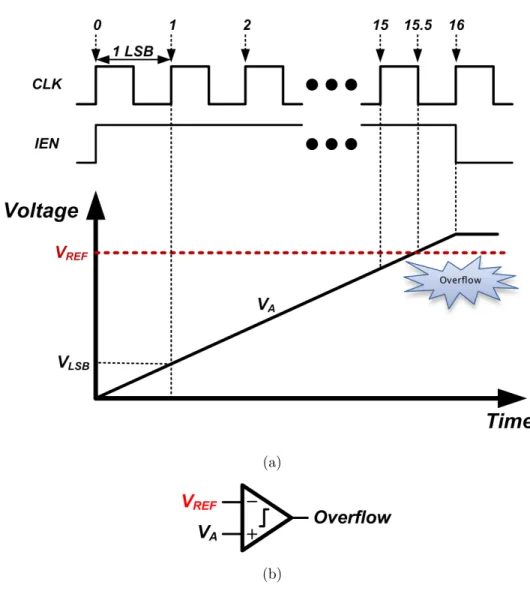
Figure 2-2: (a) An external reference clock is used to generate the enable signal IEN for the current source. When the current source is turned on, it charges the capacitor, and charging for one clock period is equivalent to adding one LSB to the capacitor. When the voltage across the capacitor exceeds the reference voltage VREF,
an overflow signal is fired. (b) The comparator block compares the charged voltage with the reference voltage.
the time when the switch is closed. When C and IREF are constant, VC becomes
proportional to TON. In the designed system, this voltage is the internal analog
variable that stores the added value.
Next, in order to make the desired TON, a time reference is needed; I simply use
a 250 kHz external clock as a global time reference. Charging the capacitor for one clock period with IREF is then defined as “adding one LSB” of a digital number, as
can be seen in Figure 2-2(a). Thus, conversion from a digital number to the analog variable VC is done by using the reference clock to generate the signal IEN in Figure
2-2(a) whose pulse width is proportional to the digital number. By enabling the current reference IREF with IEN, we can obtain VC which is also proportional to the
digital number. Note that use of “time” as an intermediate variable for conversion is advantageous because time is naturally extremely accurate.
Another component we need for the 4-bit adder is a reference voltage to indicate an “overflow” point, or the point where “the sum of the two numbers is greater than 15.” When the overflow occurs, the 4-bit adder should immediately reset itself (flush) and add the rest. VREF in Figure 2-2(a) corresponds to that reference voltage.
Its value resides in somewhere between 15 to 16 such that numbers greater than 15 generate the overflow. In order to achieve the highest noise margin, VREF should be
as close to 15.5 as possible. This issue will be discussed in detail in Section 2.5.5. Finally, an analog comparator shown in Figure 2-2(b) is used to compare the added voltage with the reference voltage and fire the overflow signal.
2.3.2
Architecture
Figure 2-3(a) shows the general form of a digital adder, where two 4-bit full adders are cascaded to become an 8-bit adder. A carry-out of the LSB (right) block is used as a carry-in of the MSB (left) block. Next, the collective analog form of the 4-bit full adder is shown in Figure 2-3(b). Note that it is one of the cascaded units. The two 4-bit digital numbers (A[3:0] and B[3:0]) and the sum output (S[3:0]) are the same as the digital adder. However, Cin (carry-in) and Cout (carry-out) signals
(a)
(b)
(c)
Figure 2-3: (a) The general form of a cascaded digital adder. (b) A 4-bit collec-tive analog adder block, showing inputs and outputs. (c) The block diagram of the designed collective analog adder.
external clock input (Clk) and request signals (Cal, Add, Read).
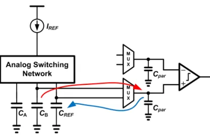
The block diagram of the designed collective analog adder implementing the block in Figure 2-3(b) is shown in 2-3(c). As can be seen in the figure, the adder is a combination of analog units and digital units: Analog units consist of a current source (IREF), capacitors (CA, CB, and CREF), an Analog Switching Network, and a
comparator. Digital units consist of a time-based digital-to-analog converter (Time DAC), a Calibration Unit, a Read Unit, and a Finite State Machine. For addition, initially, two 4-bit digital numbers to be added are stored in registers in the Time DAC. When the adder receives an “Add” pulse, the Time DAC converts those digital numbers to analog voltages by turning on the current source for some time to charge the capacitors. This charging time is implemented to be proportional to the values of the digital numbers, so the voltages added to the capacitors are also proportional to the digital numbers.
Next, the converted voltage is compared to the reference voltage which is cali-brated and stored in CREF . If the added voltage on the capacitor becomes greater
than the reference voltage, the comparator generates a pulse signal indicating an “overflow,” or “carry-out.” The reference voltage is periodically calibrated by the Calibration Unit such that the sum up to 15 does not generate the overflow pulse but the sum between 16 and 31 does. When a “Read” pulse is received by the adder, the Read Unit reads the voltage stored on the capacitor as a 4-bit digital number. Thus it operates as a simple analog-to-digital converter. Every step of these operations in this adder is controlled by the Finite State Machine. In addition, every operation is performed in an asynchronous and self-timed fashion.
2.3.3
Four Phases for Addition
In this section, I establish a procedure for addition and extend it to general collective analog computation systems.
Figure 2-4 depicts four phases required for addition and relevant waveforms in the designed collective analog adder. First of all, in the “Add” phase, the first digital number to be added is converted to an analog voltage by charging Cap A (CA in
Figure 2-4: Four phases for addition.
Figure 2-3(c)) with IREF. Then, the second number is charged on Cap A in the
same way (also in the Add phase). However, when the voltage on Cap A exceeds the reference voltage VREF, it is considered an “overflow” event. From this moment,
Cap A is reset and the rest of the voltage is charged on Cap B. This is done by the Analog Switching Network in Figure 2-3(c), which disconnects IREF from Cap A and
connects it to Cap B.
Next, in the “Carry” phase, a carry, having a value of 1 LSB, is added on the active capacitor (Cap B if overflow occurred and Cap A if not), only if an input carry exists. The overflow can also occur while adding the carry.
In the subsequent phase, the “Copy” phase, the voltage on Cap B is copied to Cap A, only if the overflow occurred during either the Add or the Carry phase so that the result is stored in Cap B. That is, if no overflow occurred, Cap B is not used and therefore the copying is not needed.
Finally, in the “Read” phase, Cap B is charged one by one until the voltage on it exceeds the voltage on Cap A. Meanwhile the number of “charging one” is counted. This process converts the analog voltage on Cap A to a digital output (sum). More detailed explanation on the reading process can be found in Section 2.5.4.
Figure 2-5: The purpose of the Copy phase is to compensate the delay error. The lost voltage during the Add/Carry phase is recovered in the Copy phase.
The Goal of the Copy Phase
One obvious advantage of having the Copy phase is that it makes the final sum to be always stored in Cap A regardless of the overflow. Thus, we can always read the value in Cap A by using Cap B. This makes the control circuit simpler and eliminates some sources of errors due to using multiple capacitors for reading.
However, the primary object of the Copy phase is to compensate the comparator delay error. Figure 2-5 depicts this point. When the comparator compares the voltage across Cap A and VREF, it needs some time to compare them and produce the result.
Consequently, switching of the active capacitor from Cap A to Cap B is delayed for some time. Since time is equivalent to voltage in the designed system, some voltage is “lost” due to this delay (minus bar in the figure), and the added result after the Add/Carry phase is smaller than the desired value. However, by copying the voltage across Cap B to Cap A, another comparison takes place. This also brings about some delay, so now some voltage is “added” (plus bar in the figure), which recovers the lost voltage.
Likewise, the input offset voltage of the comparator can be cancelled by copying, given that the settings seen by the comparator are similar for both comparisons. In this case, the sign of the error can be opposite (error voltage added during the Add/Carry phase and subtracted during the Copy phase). However, in the designed
system, the offset voltage is compensated by different methods, the digital calibration (see Section 2.5.5) and the autozeroing (see Section 2.5.2).
If we assume that the delay of the comparator is always the same, the Copy phase gives us a perfect cancellation of the error; unfortunately, the error depends on the input voltages of the comparator and the branch of the comparator (see Section 2.5.2). Furthermore, the delay error mentioned so far actually contains the digital gate delay between the comparator and the Analog Switching Network, which is also not the same in the Add/Carry phase and the Copy phase (see Section 2.4.2). However, the copying method still is a good first-order error cancellation technique that cancels most of the error.
A Generalized Computation Procedure
The sequence of the operation depicted in Figure 2-5, Add-Carry-Copy-Read, can be generally applied to collective analog computation systems. In fact, although not shown in Figure 2-5, a calibration process is needed to create the reference voltage VREF. Therefore, the generalized computation procedure can be defined as follows
(phase names in parenthesis indicate the counterparts in the designed collective analog adder).
1. Calibration (Calibrate phase): to calibrate the analog components to maintain their precision.
2. Analog core computation (Add phase): to perform moderate-precision internal analog computation, including digital-to-analog conversion.
3. External interaction (Carry phase): to interact with other units using digital-like signals.
4. Error correction (Copy phase): to correct the errors existing in the result and produce the final output (not necessarily needed).
5. Data restoration (Read phase): to periodically restore or save data by analog-to-digital conversion.
2.4
Sources of Errors
In this section, I briefly explain the sources of errors in the designed system, most of which arise from the non-idealities of the analog components of the system. This is the major challenge of this work, because they might cause serious malfunction of the system unless they are properly taken care of.
Some of the errors such as charge injection and charge sharing can be made small enough to be neglected when huge capacitors such as 1 µF are used for the computa-tion. However, it is not desirable at all because it is against the fundamental design philosophy of a collective analog system: maximum energy (and area) efficiency. In other words, it is either not suitable for integrated circuits (too big capacitor size) and not energy-efficient (high current needed to charge the capacitor). Although I increased the capacitor size during the measurement, in the design process, I aimed at using only 1 pF on-chip capacitors. The analysis of the sources of errors and the design of compensation methods are thus targeted to fulfill this tiny capacitor specification.
In section 2.5 where details of each block are explained, the sources of errors in each block will be reminded. Then, compensation methods for them will be introduced (in fact, one of the compensation methods, the copying scheme, is already introduced in Section 2.3.3). It should be emphasized again that each collective analog unit ought to be “moderate-precision,” so we need to focus more on the energy efficiency rather than the accuracy, while designing the compensation methods. The goal is to reduce the errors such that the total error in the worst case is less than the noise margin (0.5 LSB) of the system.
Finally, the summary of the sources of errors and their corresponding compensa-tion methods can be found in Seccompensa-tion 2.6.
2.4.1
Input Offset Voltage of the Comparator
Ideally, the output of the comparator should be zero if two inputs are at the same voltage. However, due to the mismatches of internal transistors and resistors
(espe-cially the input transistor pair) of the comparator, a small DC voltage (typically 1-10 mV) difference between the two inputs is needed to make the comparator output zero. This DC voltage corresponds to the input offset voltage of the comparator. Since the mismatch is more like a random process, the input offset voltage can either be plus or minus.
In the designed collective analog adder, the comparator is the core element for the computation, so it is important to take care of this input offset voltage. Otherwise, the overflow can occur outside its proper range and the output of the Read Unit can be off by one or more LSBs. The error is thus compensated by the autozeroing, digital calibration, and careful layout, as described in Section 2.5.2.
2.4.2
Comparator and Digital Gate Delay
Whenever the comparator is used in the designed system, one input voltage is held constant (VREF in the Add/Carry phase and VA in the Read phase) and the other
input voltage is increased until it exceeds that constant voltage such that the output of the comparator changes its state (from “low” to “high” or vise versa). Since the gain of the comparator is not infinite in practice, however, a very small excess voltage would not change the output of the comparator enough to be regarded as a state change (for the following digital buffer). In addition, even though the input is instantly changed to create a large excess voltage in the input, it still takes some time for a comparator to switch its output (relevant to the slew rate). These effects both contribute to the comparator delay.
Digital gates and flip-flops also create some delay. For instance, suppose the overflow occurred in the Add phase so we need to change the active capacitor to Cap B. After some delay, comparator flips its output state. This information is sent to the Finite State Machine in Figure 2-3(c) after propagating through a few digital gates. In the Finite State Machine, some flip-flops then change their states. After that, a signal is made and sent to the Analog Switching Unit, which disconnects IREF
from Cap A and connects it to Cap B. Therefore, these digital logic delays combined with the comparator delay becomes the total delay for the switching of the active
Figure 2-6: Charge sharing can ruin the voltages on the capacitor nodes.
capacitor.
The delays described here are depicted in Figure 2-5 (yellow bars with minus and plus signs) and are compensated by the copying process, as described in Section 2.3.3.
2.4.3
Sensitive Memory Nodes
The three capacitors used for computation, when not being charged by the current source, are kept “floating”. They are thus “analog memories” that hold analog volt-ages for a certain amount of time. However, the analog memory cannot hold its value virtually forever like a digital memory because of noise and leakage. Furthermore, as mentioned in Section 2.4, tiny capacitors are used in the designed system, so they are considerably more sensitive to various sources of errors.
The first source of error that can affect the capacitor node is the charge injection. When an analog MOS transistor switch is turned off, the charges accumulated in its channel are injected to the source and drain of the transistor. In the designed system, the capacitor is placed at the drain of the switch transistor. Therefore, if the amount of the injected charge to the drain is ∆Q and the capacitor size is C, the change in the capacitor voltage is ∆Q/C.
The second source of error, the clock feedthrough, is also due to the switching of the switch transistor. When the gate voltage changes abruptly between GND and
VDD, it results in the change in the drain and source voltage through the parasitic
capacitance Cgd and Cgs.
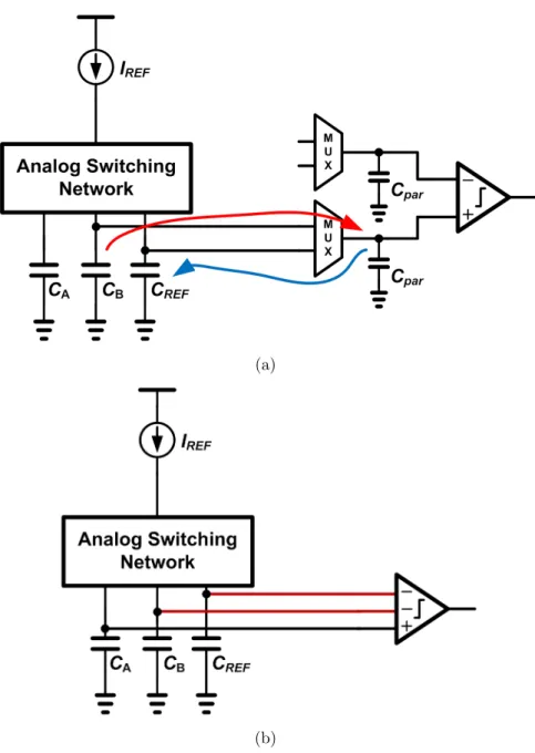
Third, the capacitor node voltage can also be affected by the charge sharing, which refers to the redistribution of charge when two floating capacitor nodes are connected. This phenomenon is depicted in Figure 2-6: According to the operating sequence described in Figure 2-5, sometimes voltages on Cap A and Cap REF are compared and sometimes voltages on Cap A and Cap B are compared. This means that some sort of “selection circuitry” is needed for the comparator inputs. Suppose we want to realize this selection by putting a multiplexer to select between Cap B and Cap REF for one comparator input, as shown in Figure 2-6. When Cap B is selected, the charge is shared between Cap B and the input parasitic capacitance of the comparator (Cpar in Figure 2-6). Next, when Cap REF is selected, the charge is
shared between Cap REF and Cpar. Thus, the voltages on Cap B and on Cap REF
will change, depending on their initial values.
Finally, due to the leakage current of the capacitor, the voltage across the capacitor decreases gradually over time. Thus it is important to periodically restore the node voltage or to convert the voltage to a digital value before the leakage error becomes significant. During the measurement, the direct contact between the capacitor node and a probe should be avoided, because it increases the leakage current.
The effect of the above sources of errors during actual measurement can be found in Figure 2-32. Various methods such as differential pair transistors, minimum size transistors, and the multi-branch comparator are used to reduce those errors, as described in Section 2.5.1 and 2.5.2.
2.4.4
Capacitor Mismatch
When there is a capacitor mismatch ∆C between two capacitors, the difference in voltage is ∆V = IT /∆C, assuming that I and T are constant. For instance, when 1 LSB is 30 mV in Cap A and Cap B is 5 % smaller than Cap A, the result of charging 15 LSB is 450 mV in Cap A and 473.7 mV in Cap B. The difference between two voltages is 23.7 mV, which corresponds to 0.79 LSB error. This amount of error is
not tolerable, because the error margin of the system is 0.5 LSB.
Thus, in order to avoid a false result at the output, this error should be taken care of seriously. Both the mismatch between Cap A-Cap REF and between Cap A-Cap B should be considered. In the designed system, the mismatch between Cap A-Cap REF is compensated by the digital calibration (see Section 2.5.5) and the mismatch between Cap A-Cap B is compensated by the common centroid layout (see Section 2.5.1).
2.4.5
Current-Source Mismatch
If we charge the memory capacitors with different current sources and if mismatch ∆I exists among the current sources, the voltage error becomes ∆V = ∆IT /C. Similar to the capacitor mismatch case, the error becomes more problematic when the value charged in the capacitor is bigger.
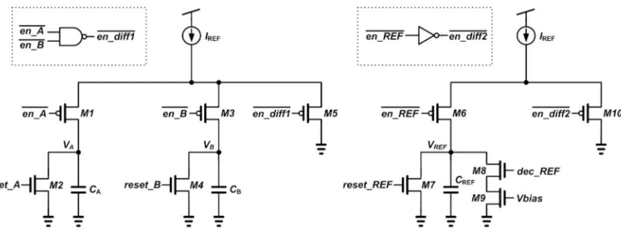
To eliminate this source of error, in the designed system, a single current source is used to charge both Cap A and Cap B (only one at a time). However, as for Cap REF, I placed another current source to charge it. This is because simulatneous charging of Cap A and Cap REF is required during the digital calibration. Therefore, as can be seen in Figure 2-8, two current sources are used to charge three capacitors in the adder. Finally, the mismatch between the two current sources is compensated by the digital calibration.
2.5
Details of Each block
This section is to provide detailed explanations on each component of the system. I start with analog parts of the system, which consist of current sources, capacitors, the Analog Switching Network, and the comparator. These parts are the kernel of the system, where the core computation (addition) takes place.
Next, digital parts are described. I first account for the details of the two units per-forming the digital-to-analog and analog-to-digital conversion, the Time DAC and the Read Unit, respectively. These converters are made in a simple and energy-efficient
Figure 2-7: An on-chip PTAT current source used in the system. Figure adapted from [15].
manner. Next, the Digital Calibration Unit which compensates several sources of errors and the Finite State Machine which takes charge of the control of the system are explained.
2.5.1
Current Sources, Capacitors, and Analog Switching
Network
Figure 2-7 shows an on-chip PTAT current source used in the designed system [15]. It generates a current of 50 nA independent of the supply voltage. The current level can vary by a few nA depending on the parameter variation, but the absolute current level is of little importance in this application. The bias voltage generated by the current source is used to mirror the current to the Analog Switching Network and the comparator. For the variability of the current level, several DAC bits are used, which can be set from the outside. The capacitors used in the current source increase power supply immunity.
Figure 2-8: The schematic of the Analog Switching Network, drawn together with two current sources and three capacitors.
capacitors. It is basically a set of switches that are responsible for the charging and discharging of the capacitors. Inputs to the switches are generated and coming from the Finite State Machine. M1, M3, and M6 are switches that are turned on to charge the capacitors, whereas M2, M4, and M7 are to discharge (reset) the capacitors. M8 and M9 are used to discharge CREF in a relatively slow rate during the digital
cali-bration. Finally, M5 and M10 are differential pair transistors of adjacent transistors that share the same current source, by which the current is always flowing through one of the branches. That is, M5 is turned on when both CA and CB are not being
charged, and M10 is turned on when CREF is not being charged.
These differential pair transistors, M5 and M10, give us two benefits. First, they maintain their source voltages to be constant, so that the currents charging the ca-pacitors also become constant. If there are no differential pair transistors, when no capacitors are being charged, those source node voltages increase almost to VDD. As
a result, next time when one of M1, M3, and M6 is turned on to charge a capacitor, initial current level is much higher than normal because initial VGS of the switch is
high (almost VDD). Thus, the use of the differential pair transistors is a trade-off
between error and power, since we are reducing the error in the current level by con-suming more static power. The other benefit is that it reduces the effect of charge injection: when the switch charging the capacitor is turned off, a certain amount of charges that were forming the channel of the transistor is dumped to the capacitor. However, at the same time, the differential pair transistor is turned on, absorbing a portion of the dumped charges.
The error due to the charge injection can also be reduced by using smaller size transistors, since the amount of the charge injection increases as the transistor size increases. The error due to the clock feedthrough is also affected by the transistor size. Thus, for all transistor switches, minimum size transistors are used (1.5 µm/0.6 µm).
Next, as can be seen in Figure 2-8, two current sources are used, despite the fact that the error due to the current-source mismatch can arise. This is to support charging CA and CREF at the same time during the digital calibration, as mentioned
in Section 2.4.5. The mismatch issue is then solved by the digital calibration, since it guarantees the correct VREF regardless of several mismatches. Between the voltage
across CA and CB, there is no digital calibration, so the same current source is used
to charge them.
The type of the capacitor used for the system is a poly-poly (two poly layers) capacitor supported by On-Semi 0.5 µm process, which has better linearity than MOS capacitors. In fact, even when non-linearity exists, it is not that problematic as long as the non-linearity is universal among all capacitors. The mismatch between the capacitors, however, should be taken care of seriously, as described in Section 2.4.4. Just like the current-source mismatch, the mismatch between CA and CREF is
compensated by the digital calibration. Thus the focus should be on the mismatch between CAand CB. In order to minimize this mismatch, 2D common centroid layout
is used, as shown in Figure 2-9. Although it depends on the process, we can generally expect the mismatch less than 3 % by this technique.
2.5.2
Comparator
In the conceptual description of the collective analog computation shown in Figure 2-2(b), a comparator is used to detect the 16th incoming pulse, i.e., the overflow point. The comparator should thus have at least 4-bit resolution to detect the voltage difference between 15 and 16. This fact reveals that the comparator is the unit that undertakes the major computational effort of the collective analog unit and determines the overall resolution of the unit. Therefore, it is important to design a reliable and energy-efficient comparator.
In the designed system, the comparator is not only used for the overflow detec-tion, but also for the digital calibradetec-tion, copying, and reading. Consequently, the comparator is also the source of various errors. Error correction methods are thus explored in this section, along with the design of the comparator.
Figure 2-10: The schematic of the comparator.
Comparator Structure with Two Negative Input Terminals
Figure 2-10 shows the schematic of the designed comparator. It is a simple two-stage amplifier, with the first stage as a preamplifier and the second stage as a high gain OTA. The preamplifier stage is to increase the input voltage difference for the second stage. However, it should be noted that the preamplifier has an “additional branch” for the negative input terminal. It exists to “select the negative input terminal volt-age” internally and avoid charge sharing.
To illustrate this point, the figure showing the cause of charge sharing in Section 2.4.3 is repeated in Figure 2-11(a). In addition, the two comparing voltages in each phase are summarized in Table 2.1. The table indicates that in all cases, either VA and VREF are compared or VA and VB are compared. First of all, since VA is
always included, we can fix VA as the positive terminal voltage of the comparator,
thereby simplifying the circuitry. Now, in this condition, a general implementation
Table 2.1: The two compared voltages in each phase Phase V + V −
Calibrate VA VB, VREF
Add/Carry VA VREF
Copy VA VB
(a)
(b)
Figure 2-11: (a) The cause of the charge sharing. (b) Charge sharing eliminated by the comparator with two negative input terminals.
that satisfies the requirements in Table 2.1 would look like Figure 2-11(a): leave the comparator and select the comparator input externally by a multiplexer. However, as shown in Figure 2-11(a), it leads to the charge sharing problem among CB, CREF,
and Cpar, the parasitic input capacitor of the comparator. Thus, external selection is
not desirable.
As an alternative, we can have “two negative terminals” and a positive terminal in the comparator and let the selection occur inside, as shown in Figure 2-11(b). Now that each capacitor node is connected to each input terminal, the node can steer clear of being spoiled due to the external selection circuitry. Furthermore, parasitic capacitance added to the node decreases, so the matching among capacitors can be improved. Inside the comparator, the selection is achieved by turning on one of the negative branches and turning off the other, as shown in Figure 2-10. Since the current required for this action is supplied by a relatively big current source, the selection is rapid and reliable.
It should be noted that in order to prevent the capacitors from interfering with each other, through the source node between the comparator’s input transistors, and to prevent the capacitors from being interfered (i.e., clock feedthrough) by the selection signal (branch enable/disable), minimum size transistors are used for those input transistors. This is in fact not common in the design of a comparator (or an amplifier), because it increases the input offset voltage of the comparator due to poor matching. Nonetheless, the top priority is to protect the sensitive capacitor node, so we need to go with the error and put an effort to compensate it.
To this end, first, common centroid layout is used for the input transistors. It de-creases the input offset by providing better matching. Second, the digital calibration method is used, which is explained in Section 2.5.5. Similar to the case of capacitor and current-source mismatches, however, this only calibrates the error between VA
and VREF. Therefore, to compensate the error between VA and VB, the autozeroing
Figure 2-12: The analog part of the designed adder with autozeroing circuitry for the comparator.
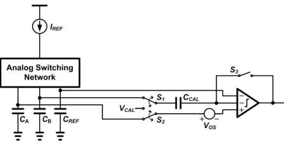
Input Offset Voltage Calibration by Autozeroing
Autozeroing is a circuit technique used to reduce the effect of the input offset voltage of an amplifier by sampling the offset to a capacitor [4]. Figure 2-12 shows the analog part of the designed adder with addition circuitry for autozeroing. It is assumed that there is an unwanted offset voltage VOS between the positive and negative terminals
of the comparator. During the autozeroing phase, both S1 and S2 are connected to
the constant voltage VCAL and S3 is closed. Since the comparator is configured as a
unity gain buffer, assuming that the open-loop gain of the comparator is much larger than one, the offset voltage VOS is sampled into CCAL. Next, during the normal
operation phase, S1 and S2 are connected to CB and CA, respectively, and S3 is open.
Since CCAL holds the same offset voltage, between the two comparing voltages (VA
and VB), the comparator operates as “offset-free.” As mentioned in Section 2.5.2,
this only calibrates the offset error between VA and VB and error between CA and
CREF is calibrated by the digial calibration.
Simulated Performance of the Comparator
Table 2.2 shows the summary of the simulated comparator specification. First, the delay of 0.09 µs is relatively small compared to the 1 LSB period of 4 µs, but it
can grow larger depending on the process variation. Thus it is still worth to have a compensation scheme for the delay, which is the copying method described in Section 2.3.3. Implementing an accurate comparator to reduce the error is in some sense an open-loop error correction method, whereas the digital calibration technique in Section 2.5.5 can be viewed as a closed-loop error correction, in that it measures the reference voltage and adjusts it until it matches with the right one.
It can also be seen from Table 2.2 that the input offset voltage of the comparator is considerable when there is a mismatch between input transistors. However, it is compensated by the autozeroing technique and the resulting offset voltage is only 3 mV (∼0.1 LSB1). The remaining offset voltage is due to the finite gain of the
comparator as well as unavoidable effect of charge injection and clock feedthrough caused by S3 in Figure 2-12.
2.5.3
Time DAC
The Time DAC functions as a digital-to-analog converter of the designed system. Interestingly, its operation is based on time. Using a clock reference and a divide-and-interleave method, it converts a 4-bit digital input to a pulse whose width is proportional to the input number. The pulse is then used as an enable signal (IEN) for the current source, as indicated in Figure 2-3(c).
Functional Description
Figure 2-13 depicts the operation of the Time DAC. When a digital input number is N-bit (N=4 in the designed system and in Figure 2-13), N clock signals are generated
Table 2.2: Simulated characteristics of the comparator
Parameter Simulated
Delay 0.09 µs
Input offset voltage (2x mismatch) 110 mV (3.5 LSB) Input offset voltage after autozeroing 3 mV (0.1 LSB)
Power consumption 12.5 µW
Figure 2-13: The simplified operation of the Time DAC.
Figure 2-14: The block diagram of the Time DAC.
by repeatedly dividing an input clock by two and the pulse width of each clock signal corresponds to the weight of each digital bit; i.e., the pulse width of the fastest clock corresponds to the least significant bit (LSB) and that of the slowest clock corresponds to the most significant bit (MSB). OUTPULSE is then generated by looking at the first pulse of each clock signal one by one. Meanwhile, whether to send out each pulse to the OUTPULSE or not is determined by each corresponding bit of the digital input. Therefore, the total “time” during which the OUTPULSE is high is proportional to the digital input value. Through the integration of the OUTPULSE, an output voltage (VOUT) that is proportional to the digital input is acquired.
Figure 2-15: The circuit diagram of the enable signal generator and the frequency divider.
Block Diagram
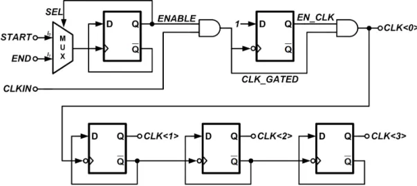
Figure 2-14 shows the block diagram of the Time DAC. When the START signal comes in from the Finite State Machine, the enable signal generator sends a gated clock signal (CLK<0>) as well as an enable signal (ENABLE) to the frequency divider. The clock is then divided a number of times in the frequency divider, as required by the number of bits (resolution). Next, the continuous interleaved sampling (CIS) block looks each of the clock signals in sequence to generate output pulses (OUTPULSE) whose total width is proportional to the digital input value. Those pulses are used to enable the constant current source (IREF) to charge a capacitor and the voltage across the capacitor (VOUT) is an analog equivalence of the digital input2.
Enable Signal Generator and Frequency Divider
Figure 2-15 is the circuit diagram of the enable signal generator and the frequency divider. When the Time DAC is not operating, the multiplexer waits for the START signal. As soon as the signal arrives, ENABLE is set high which otherwise resets all flip-flops in the Time DAC. Since the SEL bit of the multiplexer is now high,
2The current source, the current switch, and the capacitor actually belong to the analog parts
Figure 2-16: The circuit diagram of the continuous interleaved sampling (CIS) unit.
indicating the Time DAC is busy, the multiplexer blocks additional START signals and waits for the END signal coming from the CIS block. This function potentially prevents malfunction of the system due to unwanted START signals.
As described above, the Time DAC system is asynchronous and operates upon request (START signal). It is not assumed that the timing of the START signal is related to CLKIN. Thus, if CLKIN is high when ENABLE goes high, CLK GATED immediately goes high, creating a pulse in CLK<0> shorter than an the original pulse width. If CLK GATED is used directly as an LSB clock in the CIS block, this shorter pulse causes some error. To avoid this problem, a D flip-flop is added to detect the first negative edge of the CLK GATED signal. From this moment on, the clock signal for the CIS block and the frequency divider is generated. This ensures that the positive edge of CLK<0> is always lined up with the input clock (CLKIN) and the pulse widths of the two clock signals are the same.
The CLK<0> signal then is sent to (N-1) number of frequency dividers, which create N number of clock signals, CLK<N-1:0>. Representing weights of each digital bit, the clock signals are sent to the CIS block.
Continuous Interleaved Sampling Unit
The CIS unit, shown in Figure 2-16, sequentially scans through each of the clock signals coming from the frequency divider and determines whether or not to send their very first pulses to the output. Initially, when the Time DAC is disabled (ENABLE
low), the leftmost D flop-flop is set to high and other D flop-flops are reset to low. Then, when the Time DAC is enabled (ENABLE high), the leftmost tri-state buffer pair (connected to DIN<0> and CLK<0>), representing the LSB bit and LSB clock, possess the “token” so OUTPULSE becomes “DIN<0> AND CLK<0>.” Thus, if the LSB bit of the digital input (DIN<0>) is high, the LSB clock (the fastest clock) is present at the OUTPULSE. On the other hand, if the LSB bit is low, the LSB clock is ignored. However, independent of the digital input bit, the first negative edge of the LSB clock triggers all the D flip-flops, so the token is shifted to the next D flop-flop. The OUTPULSE now becomes “DIN<1> AND CLK<1>.” The same process is repeated until the last clock signal, i.e., the MSB clock. At the negative edge of the MSB clock, END goes high, which is fed into the enable signal generator and disables the whole Time DAC block. The waveforms of the clock signals and the OUTPULSE are exactly like in Figure 2-13.
Advantages of the Time DAC
Besides the simple structure and easy-to-scale property, the advantages of the Time DAC arises from the inherent accuracy of “time,” or using a clock signal as a reference: a typical crystal oscillator has an error of 100 ppm and it can even be much lower. The clock divider can also be made accurately. Thus, this structure can lead to an extremely linear DAC suitable for various applications.
The use of only one current source for charging the capacitor eliminates the po-tential mismatch issue. We can also use the same current source when we want to convert the output voltage again to the digital number. Furthermore, the current source can be used to adjust the scale factor of the DAC.
2.5.4
Read Unit
The Read Unit converts a voltage on a capacitor to a digital number. Although we can use an analog storage cell with low leakage to hold an analog voltage [11], the cost for holding an analog value grows with time. At some point, thus, it is better to
Figure 2-17: The operation of the Read Unit.
Figure 2-18: The block diagram of the Read Unit.
Figure 2-19: The Read Unit has to read differently depending on the overflow status. In order to eliminate this issue, a half LSB is added to Cap A before starting the addition.
convert it to a digital value. In addition, external signal representations of collective analog computation systems are likely to be in digital forms3, so analog-to-digital
converter is an indispensable component of the system.
Figure 2-17 reveals the operation of the Read Unit, where an analog voltage corresponding to “3” (the reason this is “3.5” in the figure is explained in the next paragraph) is assumed to be charged in Cap A. In order to read this value, I simply charge the Cap B repeatedly, 1 LSB at a time, until the voltage on Cap B becomes greater than that on Cap A. This crossing point is detected by the comparator, which fires a short pulse right at the moment. By counting the number of 1 LSB pulses before the comparator’s firing event, we can obtain the digital equivalence of the analog voltage. The simplified block diagram of the Read Unit can be found in Figure 2-18, where READ is the start signal, COMPOUT is the output of the comparator, CLK is the reference clock of the system (the same clock as in the Time DAC), 1LSBPULSE is the chain of pulses having the width of 1 LSB, and DOUT<3:0> is the 4-bit digital output of the Read Unit.
At this point, it is worth to discuss more about the number representation of the system. When setting the reference voltage VREF (overflow point), we desire it to be
15.5. The reason is that the largest noise margin (0.5 LSB) is achieved, if the overflow event happens at the exact middle of the 16th LSB charging. However, as can be seen in Figure 2-19, because of the VREF of 15.5, after the overflow, the remaining 0.5 LSB
is charged to Cap B. Thus, it can be interpreted as having an 0.5 LSB offset whenever the overflow happens. As a result, the 0.5 LSB difference in Cap A and Cap B needs to be taken into account.
It is possible to solve it by “reading differently” according to whether the overflow happened or not. However, a simpler method is to “always add 0.5 LSB to Cap A before the actual addition.” Accordingly, the overflow point should now be 16 instead of 15.5. By doing so, in both Cap A and Cap B, always an additional 0.5 LSB is stored and the Read Unit can always work in the same way, as described in Figure
![Figure 1-2: Power and area costs of analog and digital circuits. Figure adapted from [12].](https://thumb-eu.123doks.com/thumbv2/123doknet/14160003.473116/22.918.238.671.234.890/figure-power-costs-analog-digital-circuits-figure-adapted.webp)

![Figure 2-7: An on-chip PTAT current source used in the system. Figure adapted from [15].](https://thumb-eu.123doks.com/thumbv2/123doknet/14160003.473116/42.918.350.568.102.482/figure-chip-ptat-current-source-used-figure-adapted.webp)