HAL Id: tel-01242809
https://hal.archives-ouvertes.fr/tel-01242809
Submitted on 26 Sep 2016HAL is a multi-disciplinary open access archive for the deposit and dissemination of sci-entific research documents, whether they are pub-lished or not. The documents may come from teaching and research institutions in France or abroad, or from public or private research centers.
L’archive ouverte pluridisciplinaire HAL, est destinée au dépôt et à la diffusion de documents scientifiques de niveau recherche, publiés ou non, émanant des établissements d’enseignement et de recherche français ou étrangers, des laboratoires publics ou privés.
software radio transmission
Yoan Veyrac
To cite this version:
Yoan Veyrac. Design of an analog waveform generator dedicated to software radio transmission. Electronics. Université de Bordeaux, 2015. English. �tel-01242809�
software radio transmission.
Yoan Veyrac
To cite this version:
Yoan Veyrac. Design of an analog waveform generator dedicated to software radio trans-mission.. Electronics. Universit´e de Bordeaux, 2015. English. <NNT : 2015BORD0444>. <tel-01307914>
HAL Id: tel-01307914
https://tel.archives-ouvertes.fr/tel-01307914
Submitted on 27 Apr 2016HAL is a multi-disciplinary open access archive for the deposit and dissemination of sci-entific research documents, whether they are pub-lished or not. The documents may come from teaching and research institutions in France or abroad, or from public or private research centers.
L’archive ouverte pluridisciplinaire HAL, est destin´ee au d´epˆot et `a la diffusion de documents scientifiques de niveau recherche, publi´es ou non, ´emanant des ´etablissements d’enseignement et de recherche fran¸cais ou ´etrangers, des laboratoires publics ou priv´es.
présentée à
L’Université de Bordeaux
Ecole doctorale des Sciences Physiques et de l’Ingénieurpar Yoan VEYRAC Pour obtenir le grade de
Docteur
Spécialité : électronique
—————————Contribution a l’etude et a la realisation d’un generateur de signaux radiofrequences analogiques pour la radio logicielle integrale
—————————
Soutenue le : 4 Décembre 2015
Devant la commission d’examen formée de :
Dominique Dallet Professeur Bordeaux INP Président
Andreia Cathelin Docteur - HDR ST Microelectronics Rapporteur
Patrick Reynaert Professeur KU Leuven Rapporteur
Patrick Garrec Ingénieur Thales SA Examinateur
Yann Deval Professeur Bordeaux INP Directeur de thèse
Francois Rivet MCF Bordeaux INP Co-Directeur de thèse
Richard Montigny Ingénieur Thales SA Membre invité
Les travaux de thèse rapportés dans ce manuscrit sont le fruit de recherches menées au labora-toire IMS, en collaboration avec l’Université de Bordeaux et Thales.
Je tiens en premier lieu à remercier les membres du jury pour l’intérêt qu’ils ont porté à ces travaux et les échanges scientifiques pertinents
Je souhaite également remercier les différentes personnes qui ont relu le manuscrit et contribué à cette version finale.
Je remercie chaleureusement Yann, pour ces trois merveilleuses années, très riches sur le plan scientifique, culinaire et culturel. J’en garderai des souvenirs impérissables.
Je tiens à adresser mes sincères remerciements à François, pour notre étroite collaboration qui a rythmé le déroulement de la thèse dans un esprit de plaisiriosité Monkienne de tous les instants.
Merci à tous mes collègues du laboratoire IMS et de l’Enseirb-Matmeca d’avoir contribué à l’excellente ambiance de travail. Je remercie en particulier les membres de l’équipe CAS.
Un grand merci à tous mes amis, dont le fameux groupe CSI ’12 (promotion cheval), pour les très bons moments passés ces dernières années, et les nombreux autres à venir.
Je salue et je remercie mes parents pour l’ensemble de leur oeuvre, mon frère et ma belle-soeur qui m’ont promu au rang de Tonton Mouton, et ma "grande belle-soeur" adorée. J’ai passé un merveilleux premier quart de siècle dans une famille formidable, et le prochain s’annonce sous les plus heureux auspices.
Enfin, j’embrasse Pauline, ma petite puce éponyme, qui a enchanté ma dernière année de thèse et avec qui je partagerai un avenir radieux.
Introduction 21
1 Transmitters for ubiquitous network 23
1.1 Wireless communication paradigm . . . 24
1.1.1 Radio frequency transceivers architecture . . . 25
1.1.2 Wireless communication media capacity . . . 27
1.1.3 Mobile terminal transceivers compatibility . . . 28
1.2 Software radio transmitters . . . 29
1.2.1 Software radio background . . . 29
1.2.2 Directions of research for flexible transmitters . . . 32
1.3 Data conversion schemes . . . 39
1.3.1 Pulse code modulation . . . 41
1.3.2 Pulse density modulation . . . 44
1.3.3 Conversion efficiency . . . 47
1.4 Conclusion . . . 49
2 The Riemann Pump 51 2.1 Differential digital to analog conversion . . . 52
2.1.1 Differential Pulse Code Modulation (DPCM): Riemann . . . 52
2.1.2 Noise Shaping Riemann conversion (NSR) . . . 56
2.1.3 RF conversion schemes summary . . . 59
2.2 The Riemann Pump: an integrating DAC . . . 61
2.2.1 Implementation of the digital to analog integration . . . 61
2.2.2 Analog reconstruction features . . . 63
2.3 Simulation of the Riemann Pump architecture . . . 66
2.3.1 System simulation flow . . . 66
2.3.2 SNR performances: simulation results versus theory . . . 70
3 Circuits design and Implementation 83
3.1 Integration in GaN technology . . . 84
3.1.1 GaN technology . . . 84
3.1.2 Riemann Pump in GaN technology . . . 86
3.1.3 Transistor level design . . . 88
3.1.4 Simulation results . . . 94
3.2 Integration in CMOS technology . . . 97
3.2.1 Architecture in CMOS technology . . . 97
3.2.2 Core pump circuit design . . . 99
3.2.3 Riemann Pump layout . . . 109
3.2.4 Post-Layout Simulations (PLS) . . . 110
3.2.5 Chip design - PAULINA . . . 117
3.3 Conclusion . . . 122
4 Measurement results and prospects 123 4.1 Measurement results . . . 124
4.1.1 Prototypes Realization . . . 124
4.1.2 Characterization of the prototypes . . . 126
4.2 Prospects . . . 139
4.2.1 Complete transmitter architecture . . . 139
4.2.2 Riemann receiver . . . 142 4.3 Conclusion . . . 142 Conclusion 145 Publications 147 Bibliography 149 5 Annexes 157 5.1 Distribution of the slopes set . . . 158
1.1 Global mobile data traffic (source: Gartner 2015) . . . 25
1.2 Classical direct conversion transceiver architecture . . . 26
1.3 Venn diagram of the 3-dimensions wireless communication space . . . 27
1.4 Software radio transmitter architecture . . . 29
1.5 Technology tracks of 5G era . . . 31
1.6 From software defined to software radio transmitters . . . 32
1.7 Wideband DAC SotA – Conversion efficiency Vs Nyquist bandwidth . . . 38
1.8 Quantization – the DA interface . . . 40
1.9 Spectrum of an ideally sampled signal . . . 40
1.10 Architecture of overall digital to analog conversion . . . 41
1.11 Nyquist PCM DAC architecture . . . 41
1.12 Spectrum of a Nyquist rate quantized signal . . . 42
1.13 Oversampled PCM DAC architecture . . . 43
1.14 Spectrum of an oversampled quantized signal . . . 43
1.15 First order sigma delta block diagram . . . 44
1.16 First order sigma delta z–transform diagram . . . 45
1.17 Spectrum of a SDM quantized signal . . . 46
1.18 Efficiency of global digital to analog conversion . . . 47
2.1 Open loop DPCM diagram . . . 53
2.2 Closed loop DPCM diagram . . . 53
2.3 Quantization error for DPCM . . . 54
2.4 DPCM z-transform block diagram. . . 55
2.5 Noise Shaping Riemann conversion process. . . 57
2.6 Noise Shaping Riemann Z-transform block diagram. . . 57
2.7 Signal integration principle. . . 62
2.8 Riemann Pump Architecture. . . 62
2.12 Frequency response of the first-order hold. . . 64
2.13 zeroth and first-order holds impulse and freuency responses. . . 65
2.14 Matlab signal generation. . . 67
2.15 Temporal calculation of the SNR. . . 68
2.16 Spectral representation of a CW signal. . . 69
2.17 SNR Simulation chart. . . 71
2.18 SNR of the Riemann conversion versus N / r=2. . . 71
2.19 SNR of the NSR conversion versus N / r=2. . . 72
2.20 SNR of the Riemann conversion versus r / N=3. . . 73
2.21 SNR of the NSR conversion versus r / N=3. . . 73
2.22 SNR of the Riemann conversion versus frequency (r,N)=(2,3). . . 74
2.23 Piecewise linear CW spectrum – Riemann conversion. . . 75
2.24 SNR of the NSR conversion versus frequency (r,N)=(2,3). . . 76
2.25 Piecewise linear CW spectrum – NSR conversion. . . 76
2.26 First phase of the sub-6 GHz 5G spectral mask. . . 77
2.27 Spectrum of 10 aggregated channels – Riemann conversion (fs, N)=(50 GHz, 6). 79 2.28 SFDR for 10 aggregated channels – Riemann conversion. . . 79
2.29 Spectrum of 10 aggregated channels – NSR conversion (fs, N)=(50 GHz, 6). . . . 80
2.30 SFDR for 10 aggregated channels – NSR conversion. . . 80
3.1 GaN atomic composition . . . 84
3.2 GaN HEMT sectional view . . . 85
3.3 Electrical characteristics of N-type HEMTs . . . 86
3.4 Slope set generation . . . 87
3.5 Riemann Pump topology in GaN . . . 88
3.6 GaN circuit schematic view . . . 89
3.7 Top rail current generation . . . 90
3.8 Bottom rail current generation . . . 90
3.9 Switching stage . . . 91
3.10 Regulation loop . . . 92
3.11 Input buffer . . . 92
3.12 Layout view of the GaN circuit . . . 93
3.13 Power spectral density of the generated chirp . . . 95
3.17 Normalized gate capacitance of the PPA differential pair . . . 100
3.18 Static voltage characteristic of the PPA . . . 101
3.19 Bottom and top rail current sources . . . 101
3.20 Current sources characteristics . . . 103
3.21 Top and bottom rails current source characteristics . . . 104
3.22 Switching stage . . . 105
3.23 Transient behavior of the switches . . . 106
3.24 Common mode regulation loop . . . 106
3.25 Block diagram of the regulation loop . . . 107
3.26 Loop transconductance gain . . . 108
3.27 Bode diagram of the open loop transfer function . . . 108
3.28 Layout of the core pump . . . 109
3.29 Layout of the PPA . . . 110
3.30 PLS flow . . . 110
3.31 3 GHz generated CW - PLS - (a) Riemann and (b) NSR . . . 111
3.32 SFDR - PLS Vs theory - Riemann and NSR . . . 112
3.33 SNR - PLS Vs theory - (a) Riemann and (b) NSR . . . 113
3.34 Spectra of the concurrently transmitted signals - (a) Riemann and (b) NSR . . . 114
3.35 Eye patterns and constellations for the concurrent modulated signals - (a) Rie-mann and (b) NSR . . . 115
3.36 PAULINA layout view . . . 118
3.37 CKT1 Architecture . . . 119
3.38 CKT2 architecture . . . 119
3.39 CKT3 Architecture . . . 120
3.40 CKT4 Architecture . . . 121
4.1 Micro photogaph of PAULINA . . . 125
4.2 Photograph of the test board and the experimental setup . . . 126
4.3 Test bench of the standalone pump . . . 127
4.4 FPGA bit stream generator architecture . . . 128
4.5 FPGA-to-chip physical channel . . . 128
4.6 DC measurement test bench . . . 129
4.7 DC measurement input configuration . . . 130
4.11 Variation of the oversampling factor r - theoretical spectra . . . 134
4.12 Variation of the oversampling factor r - measured spectra . . . 135
4.13 Test bench of the autonomous pump . . . 136
4.14 Triangle signal spectrum and waveform . . . 137
4.15 Oscillator frequency versus tuning frequency . . . 138
4.16 Complete transmitter based on the Riemann Pump . . . 139
4.17 Digital processing and conditioning stage (concurrent generation of 2 channels) . 139 4.18 Power amplification stage topology (a) single wideband PA (b) multiple-path PA 141 4.19 Differentiating receiver based on the Riemann Pump . . . 142
5.1 Riemann reconstruction process . . . 158
5.2 Quantization error versus the relative position of the next targeted point (∆y) . 159 5.3 Intervals re-arrangement . . . 161
5.4 Frequency doubler block diagram . . . 163
5.5 Dynamic flip flops schematic . . . 163
5.6 Re-synchronization process . . . 164
5.7 Layout of the re-synchronization block . . . 164
5.8 Block diagram of the pattern generator . . . 165
5.9 Block diagram of the pulse generator . . . 165
5.10 Generation of the pulses - PLS . . . 166
5.11 Loading of the pattern data . . . 166
1.1 Performances of reconfigurable transmitters. . . 33
1.2 Performances of direct digital-RF transmitters. . . 34
1.3 Performances of all-digital transmitters. . . 36
1.4 Performances of RF-DACs. . . 38
1.5 Key features of the classical conversion schemes. . . 48
2.1 Modulation features involved in the presented conversion schemes and the related impact of the OSR on the SNR. . . 60
2.2 Features of the zeroth and the first-order holds. . . 65
2.3 Conversion architectures theoretical features summary. . . 66
2.4 SFDR versus the number of aggregated carriers - (fs, N)=(50 GHz,6). . . 81
3.1 GaN principal features for RF electronics. . . 85
3.2 Deviation of the output mean voltage with and without regulation loop. . . 94
3.3 Output impedance of various current source structures. . . 104
3.4 Features of the concurrently generated modulations. . . 113
3.5 CKT1 operating currents. . . 119
3.6 CKT2 operating currents. . . 120
3.7 CKT3 operating currents. . . 121
3.8 CKT4 operating currents. . . 121
4.1 Standalone pump operating current. . . 129
4.2 Standalone pump DC linearity. . . 131
4.3 Dual carrier spectral components - measurements versus theory. . . 133
4.4 Third harmonic level - measurements versus theory. . . 135
4.5 Autonomous pump operating current. . . 136
4.6 Triangle signal harmonic level. . . 137
AD Analog-to-Digital AC Alternating current
ADC Analog-to-Digital Converter AlGaN Aluminium Gallium Nitride
ASIC Application-Specific Integrated Circuit
BW Bandwidth
CA Carrier Aggregation
CMOS Complementary Metal Oxyde Semiconductor
CW Continuous Wave
DA Digital-to-analog
DAC Digital-to-analog converter DC Direct Current
DD Digital to Digital DFF Delay Flip Flop
DK Design Kit
DNL Differential Non-Linearity
DPCM Differential Pulse Code Modulation DSP Digital Signal Processor
DUT Device Under Test EM Electro-Magnetic
ENOB Effective Number of Bits EVM Error Vector Magnitude
FDSOI Fully Depleted Silicon On Insulate FIFO First In First Out
FIR Finite Impulse Response FM Frequency Modulation
FPGA Field Programable Gate Array FT Fourier Transform
IC Integrated Circuit IF Intermediate Frequency INL Integral Non-Linearity
I/O Input/Output
IoT Internet of Things IQ In-phase & Quadrature JTRS Joint Tactical Radio System LNA Low Noise Amplifier
LTE Long Term Evolution LPF Low-Pass Filter LSB Less Significant Bit
LUT Look-Up Table
MIPS Million Instructions Per Second MOS Metal Oxide Semiconductor MSB Most Significant Bit
NSR Noise Shaping Riemann NTF Noise Transfer Function OSR Oversampling Ratio
PA Power Amplifier
PCB Printed Circuit Board PCM Pulse Code Modulation PDM Pulse Density Modulation
PLL Phase Locked Loop
PLS Post Layout Simulation PPA Pre-Power Amplifier PSD Power Spectral Density QFN Quad Flat No-lead
QPSK Quadrature Phase Shift Keying QAM Quadrature Amplitude Modulation RADAR RAdio Detection And Ranging RC Resistance-Capacitance
RF Radio-Frequency
SDM Sigma-Delta Modulation SDR Software-Defined Radio
SR Software Radio SNR Signal to Noise ratio
SQNR Signal to Quantization Noise ratio
TSMC Taiwan Semiconductor Manufacturing Company UMS United Monolithic Semiconductors
fmax Maximum frequency of a useful signal fnyq Nyquist frequency
fs Sampling frequency of a DA conversion N Number of bits involved in a DA conversion
Pn Power of the noise Ps Power of a useful signal
q Quantum of a DA conversion scheme
r Oversampling factor: OSR = 2r
The air interface that connects the mobile terminals to the wired network is subject to a rigorous regulation enforced through various communication standards. Next generation wireless com-munications require a smart and agile use of the spectral resources to increase the data handling capacity of the network.
This trend put severe constraints on the design of mobile device transceivers. They should deal with high data rates, multiple carrier frequencies and various modulation schemes within a very restricted power budget imposed by the limited energy storage of handset terminals.
Chapter 1 exposes the radio communication paradigm and the evolution of radio transmitter ar-chitectures. It underlines the trend to increase the flexibility of the wireless transmitters through an increasing use of digital electronics according to the Software Radio principle. The major gain in flexibility is contrasted by a prohibitive energy consumption, especially within the dig-ital to analog conversion operation. The classical conversion schemes are studied and challenged.
Chapter 2 proposes the theoretical study of disruptive conversion schemes together with a suited digital to analog converter topology. It borrows the principle of Delta modulation involved in some data compression systems. The data conversion process deals with the temporal variations of the signal through a differentiating digital coding to significantly improve the conversion effi-ciency. The signal reconstruction is performed thanks to a custom integrating digital-to-analog converter named the Riemann Pump. The performances of the proposed system are assessed toward radio frequency signal generation.
Chapter 3 describes the design of the Riemann Pump in two targeted integrated technologies. The first one is a GaN technology dedicated to military applications. The second one is a 65 nm silicon technology adapted to the consumer electronics market. The design of the two circuits is detailed and post-layout simulations are presented to validate the compatibility of the proposed architecture with the chosen technologies and to assess its performances
test bench testing capabilities is required to go further in the characterization of the prototypes. Prospects are envisioned to develop a complete transceiver based on the Riemann Pump.
1
Transmitters for
ubiquitous network
Contents
1.1 Wireless communication paradigm . . . . 24 1.1.1 Radio frequency transceivers architecture . . . 25
1.1.2 Wireless communication media capacity . . . 27
1.1.3 Mobile terminal transceivers compatibility . . . 28
1.2 Software radio transmitters . . . . 29 1.2.1 Software radio background . . . 29
1.2.2 Directions of research for flexible transmitters . . . 32
1.3 Data conversion schemes . . . . 39 1.3.1 Pulse code modulation . . . 41
1.3.2 Pulse density modulation . . . 44
1.3.3 Conversion efficiency . . . 47
Chapter 1 presents the architectural trends for next generation RF transmitters. The first part introduces the wireless communication paradigm. It highlights the forthcoming requirements for handset terminal transceivers and the associated technological bottleneck. The second part presents the tracks which tend to overcome this stumbling block, in relation with the state of the art of flexible transmitters. Finally, the associated conversion schemes efficiency is questioned, claiming for disruptive approaches.
Key words: RF transmitters, Data conversion schemes, Software radio, 5G
“ The very small value of 10−16 of negentropy required per bit of information plays, however, a very important role in modern life, and it makes possible to communicate information at a negligible cost. ”
Leon Brillouin, Science and Information theory, 1956
In the 50s, Brillouin stated that modern life relies on the possibility to deal with large quantities of information for a minimal cost. In the same decade, the development of the transistor in Bell laboratories led to a physical media allowing to get closer to the theoretical cost of information described by Brillouin. After several decades during which the electronic industry endeavored to follow the Moore’s law, standalone devices that can exchange a billion of bits per second fit in one’s hand. However, conventional transceiver architectures cannot support the pressing digital convergence while satisfying customer expectations in terms of quality of service, device cost and battery life.
1.1
Wireless communication paradigm
In the 2010s, the global amount of information exchanged is still in huge growth, even though it tends to decelerate. In the same time, the proportion of mobile data is rapidly increasing; the connection to the internet becomes more and more nomadic.
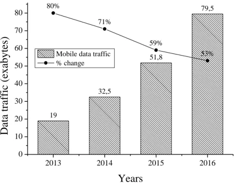
19 32,5 51,8 79,5 80% 71% 59% 53% 2013 2014 2015 2016 0 10 20 30 40 50 60 70 80
D
at
a t
ra
ff
ic (
exabyt
es)
Years
Source : Gartner 2015 Mobile data traffic% change
Figure 1.1: Global mobile data traffic (source: Gartner 2015) 1.1.1 Radio frequency transceivers architecture
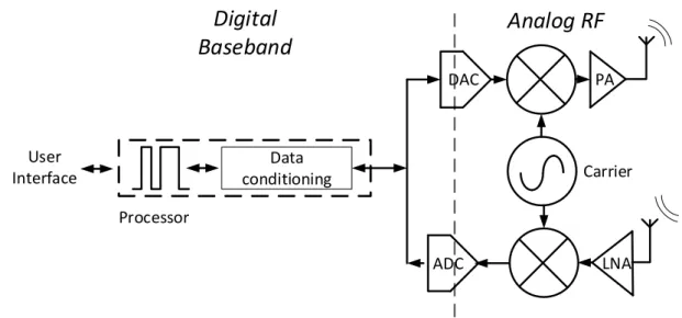
The connection of wireless terminals to the network is provided by the mean of radio-frequency (RF) electromagnetic waves. Those terminals are able to transmit and receive information car-ried at high frequencies, while ensuring the compatibility to various standards which set the traffic rules. The data to be transmitted is conditioned within the transmitter chain to be radi-ated by the antenna, while the receiver chain recovers the data from the signal picked up by the antenna. The classical simplified architecture of RF direct conversion transceivers is represented in Fig. 1.2.
The transmission chain is composed of four main blocks: • A baseband processor
• A digital to analog converter (DAC)
• A mixer to convert the signal up to the carrier frequency • A power amplifier
Data conditioning DAC PA Carrier Processor
Digital
Baseband
Analog RF
LNA ADC User InterfaceFigure 1.2: Classical direct conversion transceiver architecture
The baseband processor encodes the user digital information which is then converted into the analog domain thanks to the DAC. The analog signal is up converted to RF within the analog front-end, and then amplified and transmitted through the antenna.
The receiver chain is composed of dual blocks: • A low noise amplifier
• A mixer to down convert the signal to baseband
• An analog to digital converter (ADC)
• A baseband processor
The RF signal is picked up by the antenna, and amplified by the low noise amplifier. It is then mixed with the carrier frequency so as to recover the baseband data, which is computed by the processor and sent to the user interface. This transceiver architecture is commonly used and implemented in mobile terminals to provide a link to the network.
The growing number of connected terminals and the increasing amount of exchanged data raise congestion issues in the wireless communication space.
1.1.2 Wireless communication media capacity
The medium used to convey wireless data is the air. This medium is shared between users along three principal axes, to avoid interferences:
• Geographic areas: the wireless data transmission uses radiofrequency signals transmit-ted thanks to antennas. The received power decreases with the distance to the transmitter. The network is organized with a cellular pattern, to isolate geographic areas.
• Frequency allocation: the frequency spectrum is divided into channels dedicated to specific services. Several frequency bands are allocated to mobile communications, and those ones are subdivided into channels to handle different users at the same time. • Time sharing: communications on the same channel in the same area can occur by
sharing the time. Different portions of time are assigned to users.
Time slot
Frequency
channel
Geographic
area
Communication slotFigure 1.3: Venn diagram of the 3-dimensions wireless communication space
The intersection of those three axes defines a communication slot, depicted in Fig. 1.3. To avoid interferences, communication slots must be allocated only once. The capacity and the efficiency of a network depend on the number of communication slots offered, and its adequacy with the local needs. In order to enhance the handling capacity of the wireless network, improving the use efficiency of those three resources will be needed.
• The geographic areas obviously depend on the local density of users; cities need a finer mesh than countryside areas. The setting of cells of different size, associated with different transmitting power, allows to locally adapt the capacity of the network to the need.
• The frequency allocation is the key resource, controlled and delivered by dedicated au-thorities. Within the whole spectrum, only a few RF bands are allocated to mobile communications. Those bands are shared between several mobile access providers. Those successive divisions result in relatively narrow bands available for users, in the range of several MHz. The re-allocation of frequency bands will help to meet the need of mobile data communications.
• The time is the last dimension to be shared between users. In a same channel, multiple communications can occur thanks to time allocation. However, in the case of intense exchange of data at a given moment, the channel can be saturated. The dynamic allocation of frequency resources along time could improve the traffic fluidity. Instead of the stringent partitioning of frequency bands, those resources could be dynamically re-allocated when needed. It would grant much wider bands when the traffic is sparse, and help to fully use the resources when it is crowded.
Such a radio network is based both on smart network supervision and adaptive radio transceivers.
1.1.3 Mobile terminal transceivers compatibility
The classical transceiver architecture depicted in Fig. 1.2 suffers from a lack of flexibility inherent to the conversion performed in the analog front-end. Such a transceiver usually addresses a given standard, corresponding to a relatively narrow frequency band. However, the increase of the access bandwidth relies on the use of large frequency bands distributed all over the RF spectrum. Their introduction comes regularly with new standards and their own requirements. Mobile terminals use different transceivers to address the various standards. This trend to increase the number of parts in the chipset of mobile terminals faces pressing limits related to the industry directions and the consumer expectations.
• Bandwidth: transceivers for handsets have to support more and more data rate, on various frequency bands distributed over a multi-GHz frequency range. They have to ensure an adequate resolution over a very wide frequency band.
• Energy consumption: transceivers are one of the most power hungry part of mobile terminals. They must operate at low power to improve battery life of handsets.
• Cost: to address mass market, the transceivers should be low cost. The cost of a chip is related to the die area and the technology used.
The stacking of chips involved in the handset terminals to address different frequency bands and gather data bandwidth cannot conciliate the previous constraints. The cumulated die area of all
the transceivers turns out large, which impacts the total price of the chips and their integrability in the small volume of a handset terminal. Furthermore, enhancing the total bandwidth thanks to the addition of transceivers would substantially increase the energy consumption since the analog front-end is duplicated for each transceiver. Classical transceivers architectures suffer from a lack of flexibility and they are no more suitable for the expected ubiquitous network. Our purpose is to develop a disruptive architecture of radio transmitter that can take up the challenge.
The next section describes the evolution of wireless transmitter architectures in the past few decades, and the state-of-the-art trends and realizations that tend to overcome the requirements of tomorrow. Then, a come back to the basics of digital to analog conversion will help to apprehend the limits of the commonly used conversion schemes. It raises the need to develop innovative architectures of transmitters.
1.2
Software radio transmitters
1.2.1 Software radio background1.2.1.1 Principle
In order to meet the need of versatility raised by the new wireless communication perspectives, [1] proposed a new paradigm with the notion of software radio (SR) twenty years ago. The idea is to move the limit between the baseband domain and the RF domain within the digital processor, so as to get rid of the rigid analog front-end. The corresponding ideal architecture is depicted in Fig. 1.4.
Data processing
N
DAC
PA
Processor
Baseband
RF
The ideal SR architecture is composed of 3 blocks: • A baseband/RF processor
• A wideband digital to analog converter (DAC) • A wideband power amplifier
This architecture proposes to directly compute the modulated signal (or even a combination of multiple signals) within the digital processor, and to convert the whole transmitting band of several GHz to the analog domain thanks to a wideband converter. The output of the converter then needs to be amplified before transmission through the antenna. Software radio offers a perfect flexibility, since it is virtually compatible with all the existing standards falling into the RF domain, and any new standard can be supported thanks to a simple software update. Furthermore, it allows concurrent transmission of different standards and agile reconfiguration.
1.2.1.2 Applications
The works on software radio transceivers are motivated by many applications, involving huge markets.
Military market
The flexibility of SR transceivers finds a lot of military applications.
• Interoperability: the US military has been seeking a way to improve the ease and flexibility of communications within and between the services. A huge program called joint tactical radio systems (JTRS) has been launched, without success at the time [2]. • Secure communications: the intrinsic flexibility of SR transceivers offers a perfect
support to operate dynamic changes of the standards to secure communication links in the battlefield.
• Radar: SR transmitters are able to generate various waveforms, including radar signals. The accurate control of the waveforms allows to enhance the performances of detection [3].
• Electronic Warfare: To control the electro-magnetic spectrum in a battlefield, the use of versatile transceivers is an asset. A lot of applications rely on the use of agile signals generation (jamming, stealth, countermeasures) [4].
Civil market
The next generation of wireless communication standards (5G) is expected to offer ubiquitous immersive connectivity, relying on a software upgradable platform. Several researches on the network and communication architectures and techniques are led at the moment [5],[6]. The infrastructures would rely on an heterogeneous network with cells of different sizes [7]. The use of device to device communication is envisioned to virtually densify the network [8], and content caching to reduce data duplication [9]. As for frequency resources, 5G is expected to use as much spectrum as possible [10], divided into 3 frequency ranges for different applications (Fig. 1.5).
100 MHz
1 GHz
10 GHz
100 GHz
IOT
LTE & Wifi
evolution
New radio
access
Figure 1.5: Technology tracks of 5G era
The sub-6 GHz frequency range ensures a favorable transmission in the air; a data rate higher than 1 Gbps is expected on this band thanks to carrier aggregation. It will be based on an extension of the LTE standard and used by all the devices.
The mmW band has a reduced range and could serve in smaller cells [11], giving access to wide data bandwidth.
The internet of things (IoT) will be deployed in the same time, using the sub-GHz fre-quency band. The number of connected wireless devices will be in huge growth. Equipping those devices with reconfigurable and low-power transceivers presents a major industrial asset [12].
SR transceivers are in agreement with the implementation of those various techniques which necessitate a high flexibility. Sub-6 GHz and IoT applications are privileged targets for full software radio transmitters. Wireless communication handsets represent the most lucrative market, involving billions of units. It also constitutes one of the most challenging applications.
[13] reminds the technical and technological difficulties to reach high bandwidth and high perfor-mances at a reduced power to ensure a longer battery life, and above all with a low cost solution.
A lot of researches are oriented toward the evolution of wireless transmission architectures in the direction of flexible solutions.
1.2.2 Directions of research for flexible transmitters
Digital core
Analog Front-end
LO Mixer Processor Switch mode PA Processor Digital up conversion BB Processor Direct digital RF modulator Tunability PA PA Processor Wideband PA Wideband RF-DAC RF RF fbb DAC fbb BB fbb fc1 fc2fc3 BB RF RF
Reconfigurable
transmitters
Direct digital-RF
transmitters
All-digital
transmitters
RF-DAC based
SR transmitters
Software defined
radio
Software radio
F
le
xi
bi
lit
y
B
andw
idth
P
ow
er
consum
pt
ion
Inc
re
a
se
d
...
1.2.2.1 Reconfigurable transmitters
An intermediate step toward SR is software defined radio (SDR), where the analog front-end is reconfigurable thanks to a digital command. SDR transmitters are based on a baseband or intermediate frequency digital to analog conversion, before a final up-conversion in the analog domain. In those architectures, the reconfigurability of the analog front-end is the tricky point [14]. Various realizations of SDR transmitters are reported in the literature.
[15] proposes a software defined radio transceiver based on direct conversion with a fractional PLL, enabling carrier frequency reconfiguration. The channel bandwidth is tuned up to 16 MHz thanks to reconfigurable low-pass filters.
[16] exhibits a multiband multimode transmitter dedicated to several wireless communication standards. Multiple paths are specifically tailored to meet the precise requirements of the 2G, 3G and 4G standards; only one band group is activated at once.
[17] presents a reconfigurable monolithic transceiver working over [50 MHz - 6 GHz] frequency band. The transmitter operates with direct up conversion for the highest part of the band, and two-step up conversion for the lower part, to filter the local oscillator harmonics.
[18] exposes a SDR transmitter covering the [100 MHz - 6 GHz] band thanks to two distinct paths. The maximal signal bandwidth of 100 MHz can be used to support intra-band dual carrier aggregated signals.
Table 1.1: Performances of reconfigurable transmitters. Bandwidth (MHz) RF range (GHz) Consumption (mW) CMOS node (nm) [15] 16 0.15 – 6 100 130 [16] 20 0.7 – 2.7 200 90 [17] 40 0.05 – 6 900 130 [18] 100 0.1 – 6 103 65
1.2.2.2 Direct digital-RF transmitters
Direct digital-RF transmitters try to merge the DAC and the mixer operation, with only digital inputs. It simplifies the analog front-end and tries to give more flexibility through the increased
use of digital signals. A lot of silicon chips realizations confirm the feasibility to integrate it into handset terminals.
[19] proposes a direct digital to RF modulator to up-convert a 200 MHz sigma-delta coded base-band signal at 5.25 GHz. An auto-tuned passive base-band-pass reconstruction filter is placed at the output to cancel the digital images.
[20] implements an all-digital RF signal generator using low pass sigma delta modulation and digital mixing. It employs redundant logic and non-uniform quantization, and also proposes to use image bands to reach higher frequencies.
[21] discloses a fully digital multimode polar transmitter. It implements a cartesian to polar converter and a RF-DAC made of current-mode mixers. The local oscillator is generated thanks to a digital PLL.
[22] presents an all-digital quadrature transmitter where I and Q paths are up-converted within power cells thanks to a digital local oscillator. The two paths are then combined into a differ-ential load.
[23] addresses the issue of full duplex operation within an RF IQ transmitter. It proposes an embedded FIR filtering of out of band quantization noise to ease full duplex operation.
[24] employs a digital IQ transmission scheme with 13 bits resolution on each path. The base-band digital signals are digitally mixed and converted into the analog domain thanks to digital to RF amplitude converters.
Table 1.2: Performances of direct digital-RF transmitters. Bandwidth (MHz) RF range (GHz) Consumption (mW) Implementation [19] 200 5.25 187 130 nm CMOS [20] 50 0.05 – 1 120 90 nm CMOS [21] 4 0.9 & 1.9 250 – [22] 80 2.2 510 40 nm CMOS [23] 20 2.4 515 65 nm CMOS [24] 150 0.06 – 3.5 560 65 nm CMOS
Most of the presented works target specific standards. They propose fully integrated solutions, including the power amplification operation. However, the flexibility of the system remains lim-ited and the bandwidth and consumption performances are not sufficient to address forthcoming applications like 5G.
1.2.2.3 All-digital transmitters
Another trend consists in removing most of the analog front-end to propose all-digital architec-tures. The advancement of CMOS technologies makes digital architectures attractive [25]. The development of FPGA motivated a lot of works on the digital architectures.
[26] uses a pulse width modulation scheme to process the baseband signal and a digital IQ up-conversion to carry the signal at 800 MHz. This transmitter architecture is implemented on a FPGA and outputs a 1-bit waveform.
[27] implements an innovative digital architecture and assesses it on a very high speed data sig-nal generator. The idea is to represent a given modulation thanks to a finite state machine and to store all the possible symbol transitions in look-up tables. The baseband bit stream moves within the state machine and triggers the right sequences that are outputted as a 1-bit sequence. A sigma-delta like scheme is employed to perform noise shaping. This approach relies on heavy computational optimizations, but it supposes that the signal is representable by a finite state machine, which limits its applicability.
[28] describes an FPGA-based 1-bit all-digital transmitter using a sigma-delta modulator before digital up-conversion. It demonstrates real-time processing on an FPGA for a signal bandwidth of 2 MHz centered at 0.8 GHz.
[29] implemented a transmitter architecture with sigma-delta baseband processing and digital up-conversion. The baseband scheme is performed with an FPGA which outputs are fed to a multiplexer, together with a high speed clock generated with an external clock generator. The output is then amplified with a switched mode power amplifier.
Most of the presented architectures rely on the use of a digital 1-bit FPGA output to drive a switch-mode power amplifier, with the implementation of different kinds of digital signal conditioning. They demonstrate the interest of such digital techniques to address reconfigurable radiofrequency transmission.
Table 1.3: Performances of all-digital transmitters. Bandwidth (MHz) RF range (GHz) Architecture Implementation [26] 20 0.8 PWM FPGA [27] – 1 – 13 SDM-LUT Instrumentation [28] 2 0.8 SDM FPGA [29] 2 2.5 SDM FPGA + instrumentation
On those all-digital transmitters, the digital up-conversion is performed with a multiple of the baseband or intermediate frequency clock, so that the output RF frequency has an integer re-lationship with the working frequency. This issue has been noticed by [30]; in this reference, a sampling rate adapter is proposed. This constraint of sampling rate and carrier frequency mit-igates the flexibility of the system, especially when it comes to multi-standard and multi-band concurrent transmission. Furthermore, the total available bandwidth is limited because the con-version before the digital up-sampling is performed at baseband or intermediate frequency, often involving sigma-delta modulation.
All digital transmitters are attractive because they remove most of the analog components. The proposed architectures are easily implementable and portable to new technological nodes. However, the signal bandwidth is still limited to several tens of MHz, and most of the presented circuits are dedicated to a specific standard. The consumption of the transmitters is difficult to assess because of their implementation on an FPGA.
1.2.2.4 RF–DACs
Even though reconfigurable analog and all-digital transmitters turn out to exhibit features of software defined radio, that is, digital reconfigurability and a relative flexibility, they do not manage to deal with wideband modulated signals or concurrent transmission of a large number of signals in different bands. Those features could be offered by full software radio transmitters, giving an ideal platform to develop large cognitive radio networks [31].
To achieve this kind of architecture, the digital to analog stage has to convert the whole band of transmission, of several GHz. In this way, the complete RF waveform is transmitted, containing any combination of signals with any kind of modulation schemes and bandwidth. Referring to the software radio transmitter basic architecture (Fig. 1.4), it needs a performant digital
pro-cessing core, a wideband digital to analog converter, and a power amplification stage.
The digital to analog converter is particularly critical since it has to ensure a good signal quality over the whole RF spectrum with a low power operation. Plethora of DACs are presented in the literature, with diverse operating frequency and number of bits in the conversion.
[32] implements a 12b current-steering DAC, with specific circuit implementation to limit the mismatching and keep the non-linearities under the LSB level. A segmented architecture is chosen, with 6 binary and 6 unary weighted input bits.
[33] proposes a pseudo segmented current-steering DAC working at 28 GSps, with 6 bits, that implements a time-interleaving technique. This is one of the highest switching frequencies of the state-of-the art. The ENOB falls down to 4.6 bits for the highest part of the band.
[34] uses a 14 bits segmented architecture implemented in a BiCMOS process. Each resampling switch operates on an equivalent current source. A weighting of the 10 LSBs is done through an R-2R ladder.
[35] proposes a current steering DAC architecture, with 14 bits. It implements digital signal conditioning and high speed serialization to control the current array which outputs the differ-ential RF analog signal into resistive loads.
[36] presents a 13 bits current steering DAC working at 9 GSps. It uses specific techniques within the current cells array to reduce code-dependant output capacitance, and a pre-distortion look-up table to improve INL performances.
[37] exhibits a multimode transmitter based on a segmented current steering DAC. The high speed digital interface is embedded to feed the DAC with high speed data.
All the presented DACs except one are designed in CMOS technologies. They all implement current-steering topologies, mostly with segmented architectures. Current steering topology is known to be best suited to high speed operation [38].[39] studied the limitations of this architecture in terms of accuracy and speed, the two main characteristics of DACs. The use of time interleaving is an interesting track [40][31][41] to relax the speed of each single path. The large majority of the DACs presents a too elevated consumption for handset applications,
Table 1.4: Performances of RF-DACs. Data rate (Gsps) Resolution (bits) Consumption (mW) Efficiency (mW.s/Gbit) [36] 9 13 360 3.1 [32] 2.9 12 188 5.4 [35] 6 14 600 7.1 [37] 5 9 375 8.3 [33] 28 6 2250 13.4 [34] 7.2 14 4600 45.6
ranging from hundreds of milliWatts to the Watt level. The consumption efficiency (mW.s/Gbit) is displayed in Fig. 1.7 versus the Nyquist bandwidth of the listed DACs. It corresponds to the power consumption divided by the data rate involved in the conversion.
CMOS BiCMOS 0 2 4 6 8 10 12 14 16 0 10 20 30 40 50
Conversion efficiency (mW.s/Gbit)
Nyquist BW (GHz) [36] [32] [35] [37] [33] [34]
Figure 1.7: Wideband DAC SotA – Conversion efficiency Vs Nyquist bandwidth
The DAC realized in BiCMOS process exhibits a substantially higher consumption. The DACs realized in CMOS process are much more efficient, and they have an average conversion efficiency of several mW.s/Gbit. The resulting consumption for a 5 GHz bandwidth 12 bits DAC is around 500 mW, which is far too much for the DAC alone. The power budget of the DAC should be limited to a few tens of mW.
The broadband DAC approach to convert the whole transmitting band is still not integrable in handset terminals, because of a too high power consumption of the DAC itself.
1.2.2.5 Conclusion
Transmitter architectures tend to move from reconfigurable systems still relying on a complex analog front end to more digital solutions. Direct digital-RF transmitters and all-digital trans-mitters are in constant evolution, and they address present standards. However, the bandwidths are still bounded to several tens of a few hundreds of MHz, and the flexibility is limited. Multi-band concurrent transmission is not always supported.
The development of full SR transmitters would provide the bandwidth and agility required for the future standards. Those systems are based on high speed data processing and a suited RF-DAC. The consumption of state-of-the-art DACs is unfortunately too high to allow the im-plementation of a full SR transmitter in a handset device. A new kind of RF-DAC is needed to lower the power consumption. It requires an innovative digital to analog conversion scheme to lower the cost of conversion in terms of energy.
In the next section, we propose to come back to digital/analog conversion theory basics. The most classical conversion schemes, involved in the referenced state of the art works, are studied to underline their features toward multi-GHz operation.
1.3
Data conversion schemes
Quantization is the operation which separates the analog world from its digital counterpart. An analog signal evolves in a 2 dimensions continuous environment, where one is the time. A digital signal is made of a collection of points with discrete coordinates, thus allowing easy representation and storage. The discretization of time is associated with the notion of clock; changes can occur only on clock events. When the clock frequency is constant, the time vector can simply be an index. The binary representation of discrete quantities appears to be the most suitable to electronic implementation. The discretization of quantities thus relies on the use of bits (Fig. 1.8).
The accuracy of the digital representation of an analog signal is tightly related to the involved coding scheme. The two key parameters that drive the accuracy of a conversion are:
• the sampling frequency fs
Time
Quantity
00
01
10
11
1/f
sFigure 1.8: Quantization – the DA interface
Increasing those two parameters may result in an enhancement of the accuracy of the conversion, at the cost of a higher complexity of the system. As for the electronic implementation, this complexity induces higher component count, energy consumption, die area and design subtlety. A bandwidth limited analog signal of maximum frequency fmax can be perfectly described by an infinite resolution digital signal sampled at the Nyquist frequency (fs= fN yquist) which is twice fmax (Nyquist-Shannon theorem). That is to say the original analog signal can be recovered
without any additive noise; provided the digital signal has a perfect accuracy and the sampling images are ideally filtered (Fig. 1.9). This is theoretically achievable with an infinite number of bits to code the sampled analog levels. Such a signal would exhibit an infinite signal to noise ratio (SNR). fmax fs -fmax Frequency Spectrum amplitude fs = 2.fmax Ideal low pass filter
Figure 1.9: Spectrum of an ideally sampled signal
An actual DA conversion obviously involves a digital signal with a limited number of bits to drive the DAC. The overall DA conversion can thus be split into two distinct operations (Fig. 1.10):
• a digital-to-digital (DD) conversion that transforms the ideal digital signal into a resolution-limited digital signal at the working frequency fs
• a digital to analog converter (DAC) together with an additional low pass filter to retrieve the desired signal
DAC
LPF
∞ bits
fnyq
N bits
D-D
conversion
Digital Input
Analog
Output
fs
Figure 1.10: Architecture of overall digital to analog conversion
The most popular data coding schemes used for digital-to-analog conversion will be presented hereafter, together with the related quantization noise. Those two widespread techniques are:
• Pulse code modulation (PCM) • Pulse density modulation (PDM)
1.3.1 Pulse code modulation
1.3.1.1 Nyquist rate pulse code modulation
The most spontaneous way to encode an ideal digital signal with a finite number N of bits is to quantize each sample thanks to a N-bit word at the Nyquist frequency, with a pulse code modulation (PCM) scheme (Fig. 1.11).
N bits quantizer DAC LPF ∞ bits
fnyq
N bits fnyqD-D conversion
Digital Input Analog OutputFigure 1.11: Nyquist PCM DAC architecture
Such a quantizer disposes of 2N steps over the whole dynamic [−V, +V ]. Considering a uniform repartition of quantization levels, the dynamic is split into 2N− 1 intervals of length (2N2V−1), this
length being called the quantum q. Thus, the error eq made when quantizing an input sample
belongs to [−q/2, +q/2]. The assumption that the probability density function of eq is uniform over this interval is done, which is generally acceptable for full scale signals (e.g modulated signals) [42]. The quantization error can thus be seen as a noise with a power given by:
σe2 = Z ∞ −∞ eq2.p(eq) deq = Z q 2 −q2 eq2. 1 qdeq = q2 12 (1.1)
For a large enough N, the quantum q is approximated by 22VN, so that the power of the
quanti-zation noise is expressed as:
σe2 ≈ V2
3.22N (1.2)
This noise is in the general case considered as a white noise lying on the [−fs
2 , +fs
2 ] frequency
band [43]. For further calculations, we consider that the digital input signal represents a full scale sine wave, carrying a power σx2 of V22 once reconstructed in the analog domain. The maximum signal to quantization noise ratio (SQNR), is then calculated:
SN RdB = 10log10( σx2 σe2
) ≈ 6.02N + 1.76 (1.3)
This well-known formula is used as a reference to calculate the effective number of bits (ENOB) of converters. Such a SNR could be achieved on the analog output signal with an ideal DAC and an ideal LPF that cuts the frequencies over fmax.
fmax fs -fmax Frequency Spectrum amplitude fs = 2.fmax Quantization noise
Figure 1.12: Spectrum of a Nyquist rate quantized signal
Most common DAC architectures operate as zero-order holds which generate a staircase signal [44]. From the frequency viewpoint, the zero-order hold multiplies the digital signal spectrum by the cardinal sine function whose first zero is 2.fN yquist. This has the beneficial effect of providing a first low pass filtering which helps cutting high frequency images. However, it also causes a mild roll-off of gain at the highest frequencies of the desired band, thereby degrading the SNR. An analog low-pass filter is generally added to further attenuate the out-of-band signal, with the same harmful effect on the wanted signal. The technique of oversampling tackles this problem,
through the use of a higher sampling frequency; this opens a frequency gap between fmax and fs
2 which enables, inter alia, cleaner filtering.
1.3.1.2 Oversampling
Compared to the previously described Nyquist-rate-DD conversion, the oversampled version involves an up-sampling filter that adds samples up to a rate of 2r.fN yquist [45]. This operation
is considered as ideal, so that it provides samples with infinite resolution without adding any kind of noise. N bit quantizer DAC LPF ∞ bits fnyq N bits 2r.fnyq D-D conversion Digital Input Analog Output Upsampling filter ∞ bits 2r.fnyq
Figure 1.13: Oversampled PCM DAC architecture
The quantization noise generated by this structure has exactly the same power as before, since the quantizer exhibits the same characteristics and produces the same quantization errors. The difference comes from the repartition of the noise over the spectrum; as mentioned previously, the quantization noise behaves like a white noise for non-peculiar signals. The quantization noise power is thus uniformly distributed over the band [−fs
2 , +fs 2 ].
fmax
fs/2
-fmax
Frequency
Spectrum
amplitude
fs = 2
r+1.fmax
Quantization noise
fs
A part of the quantization noise power stands outside the wanted signal band, and is likely to be filtered out. The in-band quantization noise power is its total power divided by the oversampling ratio (OSR = 2r). Assuming an ideal low pass filtering, the maximum achievable SNR is:
SN RdB = 10log10(
σx2.OSR σe2
) ≈ 6.02N + 3.01r + 1.76 (1.4)
Oversampling thus allows a slight enhancement of the SNR by partial removal of quantization noise. It also relaxes the constraints on the analog low pass filter since it makes room to filter sampling images without altering the wanted signal; however, in this case, it reduces the amount of quantization noise filtered.
The widespread PCM DAC architecture is able to convert large frequency bands (cf. Tab. 1.4), but it turns out resource intensive to achieve a sufficient SNR, both as far as power consumption and die area are concerned. The reason is that the SNR grows preferentially with the number of bits N used to code quantized levels, and a high N implies a high component count, thereby requesting resources.
1.3.2 Pulse density modulation
Another way to encode signals is pulse density modulation (PDM), where the relative density of pulses over time represents the amplitude of the corresponding analog signal. Such a modulation can be implemented through the sigma-delta process [46]. It generally uses a one-bit quantizer that outputs a stream of ones and zeros depending on the input signal. A high density of ones corresponds to a high value of the signal and vice versa.
1 bit quantizer DAC LPF ∞ bits fnyq 1 bit 2r .fnyq D-D conversion Digital Input Analog Output Upsampling filter ∞ bits 2r.fnyq
Δ
Σ
-+Figure 1.15: First order sigma delta block diagram
The quantization error produced is fed back in the sigma-delta process so that every error is taken into account into the next sample quantization. This results in the averaging out of the quantization error, so called noise shaping. The description of this phenomenon for a DD sigma-delta modulator is usually done thanks to a linear z-transform block diagram.
+
+
Z
-1+
+
+
+
+
+
-X(z)
Y(z)
E(z)
Figure 1.16: First order sigma delta z–transform diagram
The input signal X corresponds to the output of the up-sampling filter, which is considered ideal as above; this signal is at a rate of 2r.fN yquist, with a virtually infinite resolution. The integrator
that sums the difference between X and Y is represented as an adder associated with a delay element. The quantizer is modeled by an additive noise E. The output Y can be calculated versus the two inputs, respectively the wanted signal X and the quantization noise E:
Y (z) = X(z).z−1+ E(z).(1 − z−1) (1.5)
The wanted signal is simply delayed by a sample period, whereas the quantization noise is shaped by a high pass transfer function. The total quantization noise of the system is the one of a one-bit quantizer of dynamic [−V, +V ]; it exhibits a quantum q of 2V. The quantization noise power equals q122, i.e:
σe2= q2
12 =
V2
3 (1.6)
The spectral distribution Se(f ) of this noise power for the open loop version would be uniform in the range [−fs 2 , +fs 2 ]. Se(f ) = σe2 fs (1.7) In the sigma-delta configuration, this noise is shaped instead, with the previously calculated noise transfer function. This transfer function can be expressed in the frequency domain as:
N T F (f ) = 1 − e−j2π
f
It leads to:
|N T F (f )|2 = (1 − e−j2πfsf )(1 − ej2πfsf
) = 4sin2(πf
fs
) (1.9)
The in-band quantization noise, i.e the part of the noise which lies on the frequency band [−fmax, fmax], is given as:
σn2= Z fmax −fmax Se(f ).|N T F (f )|2df = σe2 fs Z fmax −fmax 4sin2(πf fs ) df = 2.σe2[ 1 OSR − 1 πsin( π OSR)] (1.10) Assuming a large enough OSR, the Taylor series expansion of the sinus function can be used, so as to simplify the previous equation:
sin(x) ≈ x −x 3 3! + x5 5! + ... + (−1)Nx2N +1 (2N + 1)! (1.11) And, σn2≈ σe2( π2 3.OSR3) (1.12)
fmax
fs/2
-fmax
Frequency
Spectrum
amplitude
fs = 2
r+1.fmax
Quantization noise
fs
Figure 1.17: Spectrum of a SDM quantized signal
The maximum SNR theoretically achievable with an ideal low pass filtering – when the input corresponds to a full scale sine wave – is thus given as:
SN RdB = 10log10( σx2 σx2
) ≈ 9.03r − 3.41 (1.13)
It is to note that using an N-bit quantizer has the same effect as on the PCM architecture, that is enhancing the maximum SNR of 6 dB per additional bit. Compared with the PCM archi-tecture, the maximum SNR highly improves with the OSR. However, this works only under the
assumption of a high enough SNR. Indeed, in the in-band quantization noise calculation, the inversely proportional to OSR term can be cancelled by the first term of the sinus Taylor series only if the argument of the sinus is small enough. In the case of a low to moderate SNR, this assumption falls and the resulting term lowers the SNR compared with the calculated formula. This observation is relevant with all the more reason for higher order sigmadelta modulators -where the SNR depends even more on the OSR - since their principle is based on the cancellation of the successive terms of the sinus Taylor series.
This architecture is likely to be efficient for baseband signals conversion, up to several tens or hundreds of MHz (cf. Tab. 1.3). Large frequency band conversion (over the GHz range) implies a relatively low OSR because of technological limitations. As a consequence, the frequency gap between fmax and f2s is likely to be thinner than a decade, which makes it difficult to fully
benefit from noise shaping. The major problem of this topology under these conditions is that the total quantization noise does not wane as OSR is increasing, it remains constant instead.
1.3.3 Conversion efficiency
DAC
LPF
∞ bits
fnyq
N bits
D-D
conversion
Digital Input
Analog
Output
fs
Coding efficiency
(BW.ENOB)/(N.fs)
Conversion efficiency
Power/(N.fs)
Figure 1.18: Efficiency of global digital to analog conversion
The global efficiency of a digital to analog architecture mainly comes from two origins:
• The coding scheme: the efficiency of a coding scheme can be assessed through the quotient of the actual information content of the encoded signal (EN OB.bandwidth) by the data rate involved in this code (N.fs). The global data rate directly impacts the consumption and complexity of the digital processing block.
• The digital to analog conversion: the efficiency of the conversion mainly depends on the DAC topology and implementation. It can be described by the ability of the DAC to
convert a given digital data volume into an analog signal. The efficiency is thus the ratio of the power consumption and the input total data rate (N.fs).
The global efficiency of the digital to analog conversion is then the multiplication of the two described efficiencies. It is representative of the tradeoff between conversion performances (band-width, resolution), and power consumption.
The two major conversion methods are related to the two dimensions associated with quantiza-tion: time resolution and amplitude resolution.
• PDM takes advantage of time resolution; it needs a high oversampling ratio to reach the requirements in terms of resolution. It faces technological limitations in terms of maximum working frequency. Furthermore, the use of a high oversampling ratio rapidly degrades the coding efficiency.
• PCM is associated with high resolution RF-DACs. The conversion efficiency of state-of-the art DACs remains a stumbling block for handset applications.
• A combination of these approaches can be implemented with a multi-bit sigma-delta architecture. It combines the features of the two conversion schemes, with the same bottlenecks.
Table 1.5: Key features of the classical conversion schemes.
Conversion scheme Key axis Key
parameter SNR dependance (dB) Coding efficiency PCM Amplitude N 6N 12 PDM – 1 bit SDM Time r 9 1+3r2 2r+1
1.4
Conclusion
The media convergence, the user habits and the density of devices induce a huge increase of wireless data volume. Changes must occur on the network structure to bear this appetite for data. In order to ensure the compatibility with an upcoming heterogeneous and ubiquitous network, mobile terminals transceivers should satisfy the 3 major constraints:
• Low cost solution to address mass market. The flagship technology is CMOS. • Low power operation, to cope with the electrical energy storage constraints.
• High bandwidth capabilities, to enable transmission of high data rates, and to dyna-mically address existing and forthcoming standards.
SR transmitters based on the direct conversion of a wide frequency band appear as good can-didates to provide an absolute flexibility; however, the consumption of RF-DACs prevents this solution from being integrable in portable devices. The realization of a suitable transmitter needs a disruptive approach of digital to analog conversion, to improve the conversion efficiency and to overcome the bottlenecks associated with the handsets stringent requirements.
We propose to explore a disruptive approach of digital to analog conversion, invol-ving both the coding scheme and the DAC topology.
2
The Riemann Pump
Contents
2.1 Differential digital to analog conversion . . . . 52 2.1.1 Differential Pulse Code Modulation (DPCM): Riemann . . . 52
2.1.2 Noise Shaping Riemann conversion (NSR) . . . 56
2.1.3 RF conversion schemes summary . . . 59
2.2 The Riemann Pump: an integrating DAC . . . . 61 2.2.1 Implementation of the digital to analog integration . . . 61
2.2.2 Analog reconstruction features . . . 63
2.3 Simulation of the Riemann Pump architecture . . . . 66 2.3.1 System simulation flow . . . 66
2.3.2 SNR performances: simulation results versus theory . . . 70
2.3.3 Concurrent transmission . . . 77
Chapter 2 presents conversion schemes based on the digital differentiation of the encoded signal and their integration within the DAC operation. Theoretical features of those conversion schemes are studied and modeling SNR equations are obtained. The Riemann Pump is presented as the integrating DAC needed to recover the analog signal. Its reconstruction characteristics are ex-posed. Finally, system simulations are led to assess the validity of the theory with respect to the key parameters of the architecture. The application to sub-6 GHz 5G transmission schemes is highlighted and a suited sizing of the architecture parameters is proposed.
Key words: Carrier aggregation, Concurrent transmission, Differential Pulse Code Modulation (DPCM), Quantization noise, Riemann Pump, Signal to Noise Ratio (SNR), Sub-6 GHz 5G
2.1
Differential digital to analog conversion
The conversion efficiency introduced in the conclusion of Chapter 1 reflects the ability of a conversion architecture to describe an analog signal accurately with the most optimized number of digital information. All the classical conversion architectures used in the state of the art converters and transmitters rely on the absolute digital encoding of the wanted signal. We propose to encode the relative variations of the signal instead of the signal itself in order to alleviate the quantity of digital information required for the coding. It consists in operating the conversion through the derivative of the signal. The conversion scheme involved in this architecture is described in this section.
2.1.1 Differential Pulse Code Modulation (DPCM): Riemann
Differential coding schemes, such as differential PCM (or delta modulation in the case of a 1-bit quantization) are sometimes used in data compression for imaging and audio applications [47], [48]. Nevertheless, this technique remains barely used in communication systems [49], and even less in SR applications. The principle of DPCM is to quantify with N bits the relative variations of the input signal instead of its absolute value. The coded output thus represents the derivative of the signal and has to be integrated in order to recover the wanted signal.