Design, Fabrication, Testing, and Application of a
Sub-Wavelength Microwave Lens
by
Samantha M. Lewis
MASSs-c OF TECHNOL.OGYI~ NSTITUTE
MAY
112016
LIBRARIES
Submitted to the Department of Nuclear Science and Engineering
ARCHIVES
in partial fulfillment of the requirements for the degree of
Bachelor of Science in Nuclear Science and Engineering
at the
MASSACHUSETTS INSTITUTE OF TECHNOLOGY
June 2015
Samantha M. Lewis, MMXV. All rights reserved.
The author hereby grants to MIT permission to reproduce and to
distribute publicly paper and electronic copies of this thesis document
in whole or in part in any medium now known or hereafter created.
X-) Z
r
Signature redacted,
Author ...
.. ...
...
....
Samantha M. Lewis
Department of Nuclear Science and Engineering
/
Mav
8, 2015
Certified
by...Signature
redacted
Accepted by ...
'/
Richard J. Temkin
Senior Research Scientist, Physics
Thesis Supervisor
Signature redacted
Michael P. Short
Assistant Professor of Nuclear Science and Engineering
Design, Fabrication, Testing, and Application of a
Sub-Wavelength Microwave Lens
by
Samantha M. Lewis
Submitted to the Department of Nuclear Science and Engineering on May 8, 2015, in partial fulfillment of the
requirements for the degree of
Bachelor of Science in Nuclear Science and Engineering
Abstract
This thesis presents the design and experimental validation of a photonic band gap (PBG) graded-index lens. PBGs can be used to achieve sub-wavelength focusing, which is not possible with lenses made from conventional dielectric materials. Sub-wavelength focusing is attractive for a variety of applications, including medicine, optics, and mining. By creating a focal spot smaller than the traditional diffraction-limited size, higher power density can be achieved in the focal spot. Further, sub-wavelength focusing is useful in imaging applications to view objects smaller than one wavelength. Using metamaterials is a common method for creating lenses that can beat the diffraction limit, and such devices have proven to be very successful. However, metamaterials are ill-suited for high-power microwave (HPM) applications because they can have very high electric fields in the metamaterial elements that can cause breakdown. PBG structures are capable of handling substantially higher power without facing problems with breakdown or arcing. The lens presented in this thesis is an attempt to create a PBG lens capable of sub-wavelength focusing specifically for use with HPM. Testing showed the lens achieved very good sub-wavelength focus-ing near the design frequency of 2.05 GHz, with focal spot widths between 0.58-0.75 times the traditional diffraction-limited size. The lens is capable of achieving sub-wavelength focusing over a range of frequencies of roughly 400 MHz, which is a addi-tional advantage over low bandwidth metamaterial lenses. These results demonstrate significant progress in the development of novel electromagnetic materials suitable for high power applications.
Thesis Supervisor: Richard J. Temkin Title: Senior Research Scientist, Physics
Acknowledgments
I would like to thank my thesis advisor, Dr. Richard Temkin, for giving me the
opportunity to work in his lab for 3 years of my undergraduate career. He is an excellent mentor and always provided me with interesting research topics and valuable advice. I thank him for putting so much emphasis on my learning and growth as a researcher; I could not have asked for a better place to learn.
I would also like to thank my graduate student mentors, Emilio Nanni and Jason
Hummelt. Emilio was my first mentor. He made it his goal for me to learn valuable skills and understand how to conduct research. His mentorship has lasted well beyond my project with him, and I am looking forward to it continuing in the future. Jason was my mentor for this project and many others. I thank him for giving me the opportunity to choose my own projects and helping me through them as I moved towards more independent research. He is a man of many ideas and can always provide an exciting discussion.
I would like to thank Ivan Mastovsky and Michael Shapiro for their help with this
project and many others over the years. They were always available for guidance. I also thank the other members of the Waves & Beams group for welcoming me for three years. Thank you to Isaac Yandow, for helping me take my initial data over the course of many hours.
A huge thank you goes to my best friend Chamille. She has been there through
all the ups and downs of MIT, and I cannot possibly thank her enough for everything she's done. I would also like to thank my MTG family, as well, for making my MIT years brighter and making this place feel like home.
Contents
1 Introduction 10
1.1 M otivation . . . . 10
1.2 Primary application . . . . 12
1.3 Project overview . . . . 13
2 Background and Theory 15 2.1 Refractive index and dielectric constant . . . . 15
2.2 Lenses and the diffraction limit . . . . 16
2.3 Graded-index lenses . . . . 18 2.4 PBG structures . . . . 18 3 PBG lens design 22 3.1 Sim ulations . . . . 22 3.2 Fabrication . . . . 25 4 Experimental set-up 28 4.1 Probe ... .. .. ... 29 4.2 Scanner ... .. .. ... 30
5 Experimental results and discussion 31 5.1 R esults . . . . 31
5.2 D iscussion . . . . 32
5.2.2 Impact of results . . . . 36
List of Figures
2-1 Schematic of light being focused with a convex lens. The light hits the lens of refractive index n at an angle 0. This creates a focal spot of rad iu s d . . . . 16
2-2 An example of the theoretical focused beam of a diffraction-limited lens. The width, 2wo and Rayleigh range, zo, are labeled. Ellipses show contours of constant power in the focal spot. The outermost contour represents the point where P = Pmax, and the yellow contour represents P = 'Pmax. The direction of the lens axis is also shown. 17 2-3 An example of a graded-index lens. The slab acts as a convex lens,
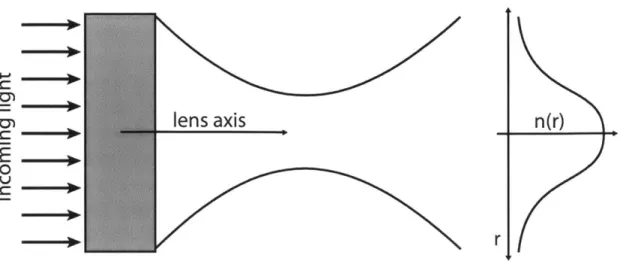
focusing the light. The refractive index n is plotted to the right as a function of r, the distance from the lens axis. The value is highest on axis and decreases outward. The profile determines the behavior of the d evice. . . . . 19
2-4 Example square (a) and triangular (b) lattices, showing the meaning of rod spacing b and rod radius a. . . . . 20
2-5 Global band gaps for rods in a square lattice for transverse magnetic field modes, as a function of the rod radius to spacing (a/b) ratio. From left to right, the points correspond to rods 1-7 of the PBG lens (see Figure 3-1). . . . . 21
3-1 Scale schematic of the lens layout, showing the meaning of the rod spac-ing b and rod radius a. The dashed lines indicate the planes of symme-try. The row and column numbers are indicated above and alongside the lens. The rod index numbers n used in Equations 3.1 & 3.2 are shown along the center row. . . . . 23 3-2 Electric field profile as simulated in CST Microwave Studio. The
mi-crowave input port is labeled, as well as the focal spot and lens. This scale is from roughly Emax to Ema, which is the range of interest for determining the 2wo spot size. . . . . 25 3-3 Plot of the magnitude of the electric field at the center of the simulated
focal spot. There are three local peaks at 1.95, 2.05, and 2.2 GHz. The highest power is found at 2.05 GHz, which was chosen as the design frequency. ... ... 26
3-4 Overhead view of the completed lens. The screws used to attach the rods are visible, indicating the positions of the rods. The upper input mounting block is also shown. The position of one of the spacing posts can be seen at the top of the photo. . . . . 27
4-1 Input head of the VNA. . . . . 28
4-2 Tip of the probe, showing the interacting wire. . . . . 29
4-3 Scanner set-up used for data collection. The end of the probe pipe can be seen outside the lens. The scanner has 3 planes of possible movement, but only two were used for these measurements. The scan directions are indicated by the x-y axes. . . . . 30 5-1 Measured width and FWHM of the focal spot at various
frequen-cies. There is some natural downward trend since, as the frequency increases, the A and the diffraction-limited sizes decrease. . . . . 32 5-2 (a) Comparison of measured width to the diffraction-limited size, A. (b)
5-3 Measured power profile at (a) 1.95 GHz, (b) 2.068 GHz, and (c) 2.2
GHz, normalized to the maximum value. The focal spot has substan-tially higher power than the surrounding area. The measured 2wo width and FWHM are shown roughly to scale. . . . . 34 5-4 (a) Power profile at 2.5 GHz. Here, there is no focusing behavior and
thus focal spot sizes cannot be calculated. (b) Power profile at 2.04 GHz. There is a focal spot, but it is less well-defined than those shown in Figure 5-3. There are strong side lobes, which dilute the low power region surrounding the spot. It is clear that the profile is less smooth at this point, indicating there is either some error, or the lens does not focus well at this frequency. . . . . 35
List of Tables
3.1 Optimum values of design parameters. These parameters together with Equations 3.1, 3.2, & 3.3 completely describe the geometry of the lens PBG structure. . . . . 24
5.1 Values of the focal spot size and comparison to the diffraction limit for the best operating points. . . . . 32
1.
Introduction
1.1
Motivation
The development of high power microwave (HPM) sources and related devices is a well-established and ever-growing field. A wide variety of disciplines depend on the use of HPM technology and consistently encourage further development. Common applications of HPM devices include radar, communication, industrial processing, and nuclear fusion experiments [1-5]. For many of these systems, the technology has been developed over decades of research and is now readily commercially available. In others, the demands placed on HPM devices encourage research using novel concepts to increase their performance and capabilities.
The development and use of metamaterials is a good example of the research that has resulted from HPM needs. Fundamentally, a metamaterial consists of a periodic structure whose period is smaller than the wavelength of light at the frequency of in-terest. Because the scale of variation is smaller than the wavelength, the metamaterial appears as a bulk material to the wave. The properties of the material that the wave sees are determined by the metamaterial design. This allows metamaterials to exhibit properties not found in nature, such as a negative index of refraction. Substantial research has been performed on metamaterials both in the microwave regime and in the optical regime. Major applications of metamaterials include cloaking, the creation of graded-index materials, improved solar power systems, and superlenses [6-11].
Conventional lenses only capture light which is propagating, but a perfect lens would also be able to capture evanescent waves. In systems like microscopes and
telescopes, this would allow for the perfect resolution of an image. Thus, the opto-electronics community has a strong interest in creating the perfect lens and exploring superlensing structures [11]. Superlenses using PBGs or metamaterials are particu-larly relevant to this work. Metamaterials and PBGs can be used to create superlenses to focus light below the diffraction limit (see Section 2.2) [12-15]. When netamaterials and PBGs operate near cutoff, they have an electromagnetic response not normally observed in natural materials, giving them the unique potential to beat the diffraction limit.
In addition, the geometrical parameters of the metamaterial or PBG can be altered to further optimize the focusing properties of the lens. This allows for a slowly varying 'effective index' inside the lens and can be exploited to optimize its focusing power. In a graded-index material, the refractive index is not constant. Instead, it is varied over the transverse dimension of the lens, causing incident light to slowly bend through the lens and focus at the focal spot. Graded-index lenses can be built from normal electromagnetic materials (i.e. glass, plastics, ceramics), but have also been created using metamaterial structures in an attempt to create a perfect lens [16].
In the microwave regime, the same principles apply. However, the use of metama-terials in high power systems is not always feasible. The small, often sub-millimeter structures can create areas of very high field which can easily cause breakdown. In these cases, photonic band gap (PBG) structures can be used [17]. These struc-tures are created from rods arranged in a lattice and are generally larger than one wavelength; thus, they are not susceptible to the same breakdown problems as meta-materials. As in metamaterials, geometrical parameters determine properties such as the effective refractive index of the structure. Variation in the geometry can be used to create a graded-index system, sometimes referred to as a graded-index photonic crystal. These structures are discussed in more detail in Section 2. By exploiting these principles, a lens created using a graded-index PBG structure could focus light
1.2
Primary application
There are a number of possible applications for such a technology, including radiation therapy systems and optical devices. A particularly interesting application is found in mining. The process of crushing and grinding rocks for mining (called comminu-tion) is highly energy-intensive. It is estimated that somewhere between 3-5% of the world's electricity is used for comminution in various industries [18]. In the US,
1.5% of electricity generation is used in such material size reduction processes [19].
The current mechanical methods employed are highly inefficient and expensive, with efficiencies less than 1% [18, 19]. Given the amount and scale of mining operations worldwide, making this process more energy efficient would both reduce electricity consumption and save money.
One novel approach to improving comminution is using microwaves to rapidly heat certain minerals within the rocks before crushing or grinding. This creates thermal stresses large enough to cause microcracks along grain boundaries in the rocks. Studies have shown that microwave heating increases the grindability by up to 70% [20]. The microcracks decrease the structural integrity of the rock, allowing it to be mechanically crushed using much less energy. These effects have been well examined for many types of minerals [20-24], and it has been shown that the the effects increase with higher power densities. This in turn requires less microwave energy input. Smaller rocks have been shown to require more energy to achieve the temperatures necessary for sufficient thermal stresses. A shorter pulse length is also more effective since it results in larger temperature gradients between the target minerals and the surrounding material [20].
Previous work in this area has primarily focused on the use of a microwave cavity to create standing waves [19]. The rock is placed in the microwave cavity for heating, which is problematic because it limits the size of rocks which can be heated to a few centimeters. This is not practical for an industrial-scale mining operation and substantially reduces the speed at which the rocks can be processed. Microwave
cavities are also typically made of materials which could easily be damaged from the harsh environment in mines [20]. Corrosion and other material damage over time would severely limit the lifetime of these devices, making them less desirable for use in industrial-scale operations. A new approach to this concept is needed in order to make microwave-assisted comminution possible at the industrial level.
The lens created for this project aims to address the problems typically found in other microwave-assisted comminution designs. The lens can be used with a pulsed microwave source, which leads to short heating times and high thermal stresses. Un-like existing microwave-assisted comminution experiments, this lens does not require a cavity. It could therefore be used on large rocks and be more readily incorporated into a mining system. The lens can be built out of stronger and harder materials like steel instead of copper, reducing its susceptibility to wear and tear from the mining environment. Most importantly, the lens uses sub-wavelength focusing to create a higher power density in the focal spot, reducing required microwave energy input. This capability makes it an attractive technology for a variety of applications.
1.3
Project overview
This project includes the simulation, design, fabrication, and testing of a graded-index photonic band gap lens. The lens was designed to achieve sub-wavelength focusing at the a certain frequency, beating the traditional diffraction limit. A number of important factors were considered in the design process.
First, the lens needed to be robust enough to operate at high power, avoiding problems with high fields and breakdown. For this reason, the PBG was designed using round rods, as the sharp edges of square rods can create unwanted high field regions.
Additionally, the lens had to be designed for a frequency where the focal spot size could be accurately measured. An accurate measurement of the focal spot size is needed to validate the focusing behavior of the lens and thus the lens was designed at
a lower frequency. At high frequencies, the focal spot size would become very small and therefore difficult to measure accurately. The larger spot size allows for a higher resolution of measurements in and around the focal spot, improving the accuracy of the results.
Further considerations were addressed in the actual fabrication of the lens. Several alterations were made to the lens structure over the course of the design process in order to make it easier to fabricate. Other alterations were made to ensure that the lens would be appropriately rigid. Since the PBG behavior is highly geometrically-dependent, the fabrication tolerances on the rods had to be fairly small. Of the various fabrication methods examined, the direct machining was deemed the best at satisfying these and other practical constraints.
Testing the lens created a number of demands. The focal spot size can only be determined by constructing a power profile. This was done by measuring the transmitted power from an input waveguide at equally spaced positions in the area surrounding the expected focal spot location. A probe had to be created which could measure the power inside the small vertical height of the lens. Very sensitive equipment had to be used in order to measure the power even with low coupling to the probe. To keep measurements consistent and accurate, a motorized scanner set up had to be used to change the probe's position. Each of these experimental solutions
2.
Background and Theory
This section will cover the relevant theoretical and technological information necessary to describe this project. It includes a brief discussion of refractive indices, dielectric constants, diffraction, and lenses. It also includes more information on the design
and function of graded-index lenses and photonic band gap structures.
2.1
Refractive index and dielectric constant
The refractive index (or index of refraction) of a medium is a unitless expression of how light behaves when it propagates in the medium. It can be expressed as the ratio of the speed of light to the phase velocity of light in the medium, n = V. It can also be expressed as a function of relative permittivity c, and relative permeability
Pr, which are related to the electric and magnetic behavior of the wave as described
in Maxwell's equations. The relative permittivity, often referred to as the dielectric constant, is simply the ratio of the electric permittivity of the medium to the vacuum permittivity, co. Similarly, y, is the ratio of the magnetic permeability of the vacuum permeability po.
The relation of these quantities to the index of refraction is n Cr/J.
Conven-tional, natural materials have positive refractive indices. In many metamaterial and PBG research efforts, the goal is to create materials with negative n.
2.2
Lenses and the diffraction limit
In the most general sense, a lens is simply a structure which is used to change the path of light. In the case of a convex lens, the light is focused to a focal spot. While lenses are most familiar in the optical regime where they're used in common devices like cameras and eyeglasses, they can be constructed in any frequency regime. At any frequency, there is a fundamental limit imposed on the focal spot size due to diffraction. Even with no other losses, a traditional lens cannot focus light to a spot smaller than this limit. This imposes restrictions on the possible resolution of devices like microscopes and telescopes. A general expression for the diffraction limit is
d =- 2n sin ', (2.1) where d is the radius of the resolved spot, A is the wavelength of the light, n is the refractive index of the medium, and 0 is the angle of the incident spot [25, 26]. In the
case of a lens with n = 1 and a 90 degree incident angle (see Figure 2-1), this reduces to d
incoming
light
lens
--d'
--
-
focal spot
Figure 2-1: Schematic of light being focused with a convex lens. The light hits the lens of refractive index n at an angle 0. This creates a focal spot of radius d.
An example focal spot is shown in Figure 2-2. The size of the focal spot is defined by two dimensions: the width 2mo, and the length along the lens axis direction, known as the Rayleigh range zo. In the remainder of this work, the 'width' of the focal spot will always refer to 2 0o, the full size of the spot in the direction perpendicular to the
lens axis (see Figure 2-2). An edge of the focal spot can be defined by the points where the power P = 2Pr,,. Here, Pmao is the maximum power, located in the center of the focal spot. The width and Rayleigh range are neasured using this edge. Another useful description of the focal spot size is the full width at half maximum (FWHM). The FWHI-M is measured in the direction perpendicular to the lens axis from the points where P =Pma0 . Both size definitions are shown on the example focal spot
in Figure 2-2. A diffraction-linited focal spot, has 2m = A and FWHM = [25, 26].
Lens
0
--
+
Peak intensity
Focused light
Figure 2-2: An example of the theoretical focused beam of a diffraction-limited lens. The width, 2w() and Rayleigh range, zo, are labeled. Ellipses show contours of constant power in the focal spot. The outermost contour represents the point where P
2Pmax, and the yellow contour represents P = 'Pmlr. The direction of the lens axis
is also shown.
In order for a lens to beat the diffraction limit, the focal spot must have a width of less than A and a FWHM of less than A. Beating the diffraction limit would allow better performance in a wide variety of devices. A smaller focal spot has higher power
density, which is useful in applications where the power must be delivered to a small region, such gamma radiation therapy. Optical devices like microscopes would be able to resolve objects smaller than one wavelength, and as small as the focal spot width.
Beating the diffraction limit and achieving sub-wavelength focusing can only be done using a lens with a non-traditional index of refraction. Possible solutions include using negative graded-index materials or photonic band gap structures to create a lens with a negative index of refraction or graded-index profile. These topics are explored in the following sections.
2.3
Graded-index lenses
Graded-index devices are structures in which there is a gradient of the refractive index with position. A gradient can be created with traditional, positive refractive index materials. In these cases, the refractive index is usually largest at the center and gets smaller towards the edges of the device (see Figure 2-3). Negative graded-index structures can also be created. In these devices, the modulus of the refractive index is smallest at the center axis of the device and increases outward. This allows the device to behave as a convex lens and focus a plane wave [27]. The graded negative index profile creates a number of interesting focusing effects, such as superlensing
[28-31]. It is possible to create a negative graded-index structure through the use of
metamaterials and PBG structures [12-15]. For the reasons discussed in Section 1.1, PBG concepts were used as the basis for creating the negative graded-index structure for this project.
2.4
PBG structures
A photonic band gap structure consists of a periodic lattice of metal and/or
_lens
axis
n(r)
E
0
r
Figure 2-3: An example of a graded-index lens. The slab acts as a convex lens, focusing the light. The refractive index n is plotted to the right as a function of 'r,
the distance from the lens axis. The value is highest on axis and decreases outward. The profile determines the behavior of the device.
air/vacuum gaps. This variation of the dielectric constant creates band gaps: any wave with a frequency within the band gap cannot propagate through the lattice. In the case of incident waves, the wave is reflected. PBG cavities can be created by removing rods to form a defect in the lattice. In these cases, the disallowed mode is confined in the defect region while other modes propagate out. Band gaps profiles for cylindrical rods in triangular and square lattices have been calculated and are well-documented [17, 32, 331. The size, arrangement, and material composition of the rods all affect the frequency and mode selectivity of the PBG, allowing the design of highly selective structures [17].
Figure 2-4 shows example square and triangular lattices as well as useful defini-tions of PBG geometrical parameters. Figure 2-5 shows the band gap maps for these lattices, calculated by [32]. These band gap maps show the areas of disallowed nor-malized frequency with respect to the ratio of the rod radius (a) to rod spacing (b). The disallowed regions are located to the right of the curves if Figure 2-5. Within one lattice, a and b can be varied, thereby moving to a new location in the band gap map.
By crossing into or out of a band gap, the refractive index changes. Thus by varying
the size and/or spacing of rods, a graded-index photonic crystal can be created as
discussed in Section 2.3. These band gaps are calculated for the theoretical case of an infinite lattice. The band gaps for a finite lattice will be slightly different. However, it has been shown that PBG structures can achieve high performance with only a few rows of rods.
0
b
b
(a)
Figure 2-4: Example square (a) rod spacing b and rod radius a.
0
Y-00
b b
and triangular (b) lattices, showing the meaning of
20.C
I,15.01-.010.0
5.0
0.01
0. 0
f roI I I I I I I I I I IiI.0.1
0.2
a/b
0.3
0.4
0.5
Figure 2-5: Global band gaps for rods in a square lattice for transverse magnetic field modes, as a function of the rod radius to spacing (a/b) ratio. From left to right, the points correspond to rods 1-7 of the PBG lens (see Figure 3-1).
0
0
3. PBG
lens design
The section details the process of designing the lens including challenges that were faced. It also contains an explanation of the final lens design and its predicted per-formance.
3.1
Simulations
The physics problems describing PBG performance are not easily analytically solv-able. Thus in order to design and optimize this structure, it was necessary to use simulations. The simulations were performed using CST Microwave Studio, a com-mercially available software package for microwave device simulation [34]. The goal of the simulations was to determine the optimum number of rods as well as their size and spacing.
While PBG theory treats PBG lattices as infinite, in practice these devices gen-erally only require a few rows of rods (a few periods) to achieve the desired perfor-mance. The optimum number was determined to be 7 rows with 14 rods in each column. Adding additional rows or columns beyond this point did not significantly improve the focusing capabilities of the lens. The lens has mirror symmetry across a plane through the fourth row as well as a plane between the 7th and 8th columns
(see Figure 3-1).
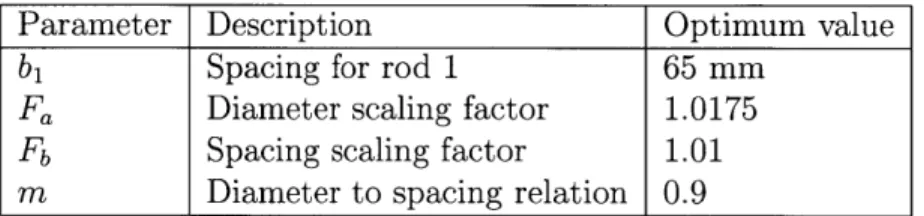
Once the necessary number of columns and rows was determined, five parameters were adjusted: a, the spacing of the rods; b, the diameter of the rods; Fa, a scaling factor for the spacing; F, a scaling factor for the size; and m, a factor which
deter-0
3
S S4
0 05
00
6
S7
0
8
S0
, 1 ,
,
S
0
S I
4--- -0-- - *- -0- -e--0-0
9
010 11
12
0
0
0
S
0
13
0
0
0
0 0*
*
1
23
4
5
-0-14
0
0
5,
6
0
7
0
0 S*
*
0 0 15 0 **
0 0*
*
0 0 S0
0
0
*
*
b
S
00
*a
Figure 3-1: Scale schematic of the lens layout, showing the meaning of the rod spacingb and rod radius a. The dashed lines indicate the planes of symmetry. The row and
column numbers are indicated above and alongside the lens. The rod index numbers
n used in Equations 3.1 & 3.2 are shown along the center row.
mines the relationship between the spacing and diameter. The values of F and F
are constant over the structure, but a and b change with each column in order to create a gradient in the refractive index over the structure. All the rods in a given column have the same a and b. The formulas describing a and b are
a, = a(,,>F 2(n-1) (3.1)
and
(3.2)
where n = 2, 3, ... 7 corresponds to the number of the rod counting from the center of
the lens. The spacing of the first rod, a,, is given by the formula
a
-a, 5
(3.3)1
10
2
020
30
*
0
6
7
- -- --- I - - - Awbn
=b(n_1)
F2 n-1The formulas for a, and b, were chosen because they provide a simple way to change the values of a and b with each column. The only scaling factors are Fa and F, which provides more control in attempting to find optimum values. This was preferable over having a more complicated function like a quadratic polynomial with multiple scaling factors. For each simulation, the values of bi, Fa, F, and m were chosen, allowing all other values to vary based on these factors.
In simulating the lens, the goal was to find the values of these parameters that resulted in a high peak value of the electric field and a focal spot width smaller than the diffraction-limited size. After numerous simulations, optimum values of these parameters were chosen. The optimum was considered to be the point where the focal spot width was less than 0.65 times the diffraction-limited size, and the electric field at the center of the probe was at least 1000 V/m at a frequency between 1.7 GHz and 2.3 GHz. This frequency range was chosen in order to make future testing possible with existing lab equipment.
Comparing simulations with varied values of bi, Fa, F, and m made clear which values produced results closest to the optimum conditions. Iterations were performed until all factors were chosen. They are summarized in Table 3.1.
Parameter Description Optimum value
b1 Spacing for rod 1 65 mm
Fa Diameter scaling factor 1.0175
Fb Spacing scaling factor 1.01
m Diameter to spacing relation 0.9
Table 3.1: Optimum values of design parameters. These parameters together with Equations 3.1, 3.2, & 3.3 completely describe the geometry of the lens PBG structure.
Field profile for the chosen design is shown in Figure 3-2. The peak power is found at a frequency of 2.05 GHz, with smaller peaks at 1.95 and 2.2 GHz (see Figure
3-3). The 'design frequency' of this lattice is 2.05 GHz, as that is the point with the
maximum power. For this frequency, the width of the focal spot is approximately
82.7 mm. The diffraction-limited focal spot size can be calculated using Equation
times the diffraction-limitted size. In all simulations, the height of the rods was 2 mm. When constructing a lens, a larger value had to be chosen in order to make fabrication feasible. The value was chosen to be 20 mm. New simulations were run with a rod height of 20 mm and the focal spot width was not affected.
E (V/M)
H
1200 1100 1000 900 800 700 600 500 443Figure 3-2: Electric field profile as simulated in CST Microwave Studio. The mi-crowave input port is labeled, as well as the focal spot and lens. This scale is from roughly 'Emax, to Ema, which is the range of interest for determining the 2wo spot size.
3.2
Fabrication
Each piece of the lens structure was direct machined in aluminum, which was chosen to minimize the cost and weight of the lens. The focusing behavior of the lens is not contingent on the material and losses at this frequency are small, so the lens could be built out of steel or a variety of other metals. In choosing a fabrication method, 3D printing was also considered. There are two main options: making the device purely from metal using Direct Metal Laser Sintering (DMLS), or 3D printing a. plastic
-0 0 -0 1000-800-- - -600 400 200 _ _ _ _ _
[
_ 1.9 2.0 2.1 2.2 2.3 2.4 2.5 Frequency (GHz)Figure 3-3: Plot of the magnitude of the electric field at the center of the simulated focal spot. There are three local peaks at 1.95, 2.05, and 2.2 GHz. The highest power is found at 2.05 GHz, which was chosen as the design frequency.
structure and adding a metal plating. Both of these options are readily available and could have been used to construct this device. However, it was determined that the components of the 2D structure were simple enough to machine directly. For a more complicated design or one which has variations in 3 dimensions, 3D printing would be a superior choice.
The structure itself consists of two large, thin, metal plates which serve as the top and bottom of the lens. They lie in the same plane as the overhead view of the rod layout in Figure 3-1. The rods have tapped holes through their centers and are attached directly to the plates on both sides to ensure good alignment. Originally, the rods were designed to sit in recessed pockets in the plates. However, this is more complicated to machine and would require thicker plates. It would require narrow fabrication tolerances on both the rods and the pockets to ensure the lens could be assembled correctly. Screwing the rods directly to the plates makes the lens simpler to machine by eliminating the need to create pockets of varying sizes. Additionally, the cost and weight of the lens can be reduced using this method. The metal plates are the largest physical parts of the lens and therefore make up most of the weight.
By not requiring pockets, thinner plates can be used. Using this method does not
depth of the rod. A rod with a tapped hole and screws inside appears the same as a solid rod to the wave as long as the size of the rod is not comparable to the wavelength. All of these factors contributed to the decision to attach the rods via screws.
The plates had to be long enough to contain the field area shown in Figure 3-2. Because of this, there are large sections of the top plate which are not supported
by any rods. To address this., a spacer post was added to each of the four corners.
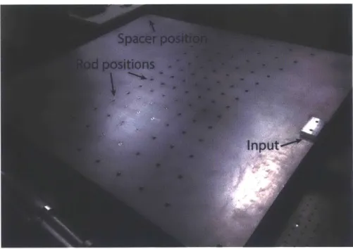
This provides support to the top plate to reduce stresses and eliminate bending. Two mounting brackets were designed to provide a place to attach equipment needed for testing. These were placed on the top and bottom plates on the input side of the lens. The input side (from where the input wave is launched) is on the end of the plate closer to the PBG lattice. The completed lens can be seen in Figure 3-4.
Spacer
position-d
positions-Input
Figure 3-4: Overhead view of the completed lens. The screws used to attach the rods are visible, indicating the positions of the rods. The upper input mounting block is also shown. The position of one of the spacing posts can be seen at the top of the photo.
4.
Experimental set-up
In order to determine the size of the focal spot, it was necessary to measure the power profile of the lens. To do this, the lens was connected to an Agilent E8363B vector network analyzer (VNA). Waves were launched into the lens using an S-band microwave head from the input side of the device, closer to the rods (see Figure
4-1). At the other end, a probe was inserted to measure the transmission (S1 2). This
measurement was repeated at varying positions in order to construct the power profile.
4.1
Probe
The simple probe constructed for the power measurement consists of a small length of exposed wire, bent to be parallel with the electric field orientation. This wire is connected to an SMA cable which runs through a rigid pipe. The length of the interacting wire is 9 mun, a substantial portion of the 20 nn rod height. The probe is shown in Figure 4-2. The rigidity of the pipe ensured that the probe remained in
good alignment with the electric field orientation as its position varied. In order to
prevent reflections caused by the metal pipe, the probe is wrapped in ECCOSORB shielding.
4.2
Scanner
Since the ooal of this measurement was to examine the dependance of the electric field on probe position, it was necessary to obtain a high resolution of points over a large area of the lens. Manual movements of the probe are too inexact and cumbersome to provide useful data. Instead, a motorized scanner set-tip was used. The probe was fixed to the motorized stage which was then moved in steps over a specified area. The scanner recorded an S1 measurement at a specified frequency through the VNA. This
allowed for easy adjustment of the measured frequency. step size, and scan area. The scanner set-up can be seen in Figure 4-3. Scans were taken at a variety of frequencies surrounding the design frequency of 2.05 GHz. This was done in order to demonstrate the minimization of the focal spot width near the desired frequency.
Scanner set-up
Probe
-Figure 4-3: Scanner set-up used for data collection. The end of the probe pipe can be seen outside the lens. The scanner has 3 planes of possible movement, but only two were used for these measurements. The scan directions are indicated by the x-y axes.
5.
Experimental results and
discus-sion
5.1
Results
Scans of the power profile in the lens were taken to determine the focal spot size at various frequencies. Points were chosen surrounding the design frequency of 2.05 GHz as well as farther away in order to show the difference in focusing performance with frequency. At each frequency, the focal spot width and FWHM were calculated (see section 2.2) and compared the corresponding diffraction-limited values at that fre-quency. The ratios of the measured values to the diffraction-limited values determine whether the lens beat the diffraction limit. The measured sizes are shown in Figure
5-1, and results of the ratio calculations are shown in Figure 5-2.
Overall, the lens was able to beat the diffraction limit at all measured frequencies, a range of 400 MHz. The spot size is smallest in the area surrounding the design fre-quency, but is still measurably smaller than the diffraction limit at other frequencies. The best performance is found at 2.068 GHz, 1.95 GHz, and 2.2 GHz. The latter two frequencies correspond to the smaller peaks in power predicted by CST simulations (see Figure 3-3). The first appears to be a slight shift from the design frequency and peak power point of 2.05 GHz. The measured power profiles at these three frequencies are shown in Figure 5-3 along with their 2wo and FWHM sizes. Table 5.1 summarizes data at these frequencies.
150 140t 130- 120-110 10090 -N 80 70 -60 50 -40 1.90 1.95 2.00 2.05 2.10 2.15 2.20 2.25 2.30 Frequency (GHz)
Figure 5-1: Measured width and FWHM of the focal spot at various frequencies. There is some natural downward trend since, as the frequency increases, the A and the diffraction-limited sizes decrease.
2mo FWHM
Frequency (GHz) Size (mm) Fraction of limit Size (mm) Fraction of limit
1.95 90 0.585 55 0.715
2.068 92.5 0.638 50 0.689
2.50 82.5 0.605 47.5 0.697
Table 5.1: Values of the focal spot size and comparison to the diffraction limit for the best operating points.
5.2
Discussion
This lens focuses well below the diffraction limit for the frequencies examined. These results mark substantial progress in the effort to create a lens for HPM applica-tions which is capable of sub-wavelength focusing. This experiment has validated the performance of this lens design over the frequency range examined. There is still op-portunity to examine more frequencies, though from simulations there is little reason to believe there will be more high-performance points.
Attempting to evaluate the lens far from its design frequency presents difficulties.
C 2w0 0 FWHM 00 0 00 0 00
1.0 0.9 2w 0.8 C0.7 - -0.5 1.90 1.95 2.00 2.05 2.10 2.15 2.20 2.25 2.30 Frequency (GHz) (a) 0.9 - 0 OD 0.8 - 0 0 4-.0 0 0
t0.6
U-1.90 1.95 2.00 2.05 2.10 2.15 2.20 2.25 2.30 Frequency (GHz) (b)Figure 5-2: (a) Comparison of measured width to the diffraction-limited size, A. (b) Comparison of the measured FWHM to the diffraction-limited size,
y.
For frequencies near the design frequency and high power spots, the width and FWHM measurements are good indicators of the focusing quality. They are most useful when there is good focusing behavior. Figure 5-4 shows two examples of frequencies where these metrics are less useful. At 2.5 GHz, there is little to no focusing and thus no real focal spot is formed. This was predicted by simulation: in Figure 3-3, it is clear there is very little field at the center of the expected focal spot position. Since there is no focal spot, no width or FWHM can be measured and therefore the frequency cannot be compared to others on that basis. This frequency can be deemed beyond the operating range of the lens.
At 2.04 GHz, the difficulties are riot so immediately apparent. A focal spot is formed, but the focusing behavior is poor. The resulting power profile is less smooth
15 x position (cm) (a)
.I
1.0 0.9 0.8 30 25 0.7 -E 20 0.6 0.5 15 0.4 0 >,1 U.3 0.2 0.1 5 x position (cm) (b) 00
30 25 20 15 10 5I
0.8 0.7 0.6 0.5 0.4 0.3 0.2 0.1 5 10 15 20 25 x position (cm) (c)Figure 5-3: Measured power profile at (a) 1.95 GHz, (b) 2.068 GHz. and (c) 2.2 GHz, normalized to the maximum value. The focal spot has substantially higher power than the surrounding area. The measured 2w0 width and FWHM are shown roughly
to scale.
than that of a well-focused frequency. Further, there are side lobes next to the focal spot which are at high power in comparison to center of the spot. These alter the edge of the focal spot. making it difficult to use the 2w0 definition of width. In
these cases, the FWHM is a much better indicator of the focal spot size because the
30 25 20 u 0 -7 15 0 10 5
I
1.00.9 0.8 0.7 0.6 0.5 5 10 )0.4 0.3 0.2 0.1I
3 1.0 30,1 1.0 0.9 0.9 25 25 0.8 -0.8 0.7 0.7 0.6 0.6 0 15 0.5 151' 0.5 >10 0. ,100. 0.2 0,2 5 5 0.1 0.1 5 10 15 20 25 5 10 15 20 25
x position (cm)
x position (cm)
(a) (b)Figure 5-4: (a) Power profile at 2.5 GHz. Here, there is no focusing behavior and thus focal spot sizes cannot be calculated. (b) Power profile at 2.04 GHz. There is a focal spot. but it is less well-defined than those shown in Figure 5-3. There are strong side lobes, which dilute the low power region surrounding the spot. It is clear that the profile is less smooth at this point, indicating there is either some error, or the lens does not focus well at this frequency.
center of the focal spot is still well focused. This can be seen in the data for 2.04 GHz in Figure 5-1 and 5-2. The FWHM\ varies as expected, with a small decrease due to the difference in wavelength. and a substantial change near the design and high performance frequencies. The 2wo width is less consistent, in that there are frequencies where the 2wo value does not vary in the same manner as the FWHIM. At 2.04 GHz, the 2w0 is much smaller than the values at the next largest frequencies,
while the FWHM size roughly follows the expected pattern. These anomalies arise from attempting to measure the 2wo width of a poorly focused spot.
Interestingly, the Rayleigh ranges of the focal spots, even at the best frequencies, are shorter than simulations predicted. The highest power is concentrated into a nearly circular region, rather than an oblong region as expected. It is possible that this is the result of sonie fabrication error, but further studies are needed to conclude the source of this difference.
5.2.1
Potential sources of error
PBG designs are highly frequency-selective by nature and their operating frequencies are determined by geometry. Because of this, small fabrication errors can result in a shift of the operating frequency in a PBG device. It is likely that the shift of the high power point from 2.05 GHz to 2.068 GHz is due to a fabrication error.
It is also possible that there is error in the values of the width and FWHM. The data has a limited resolution, and therefore the measurements could be off by as much as 2 mm from lack of resolution. This error can be reduced by taking data at a higher resolution, which is possible using the scanner set-up, but not time-effective when examining a large amount of frequencies. There could be systematic error introduced in the measurements from a tilt or misalignment in the probe. The device is also subject to reflections, which was observed before the probe was shielded. It is possible that objects far outside the lens could reflect and influence the field patterns, though the effect would likely be small.
An error in the measured focal spot size could impact the relative attractiveness of various operating points. However, the lens beats the diffraction limit substantially at all points of interest. Therefore, even with an error on the order of 10 mm (much higher than any of these factors could contribute), most of the frequency points still beat the diffraction limit.
5.2.2
Impact of results
This lens clearly demonstrates sub-wavelength focusing capabilities over a range of frequencies. This is an important result for potential HPM applications, where the use of a PBG structures is heavily preferred over metamaterials because of their superior performance under high power conditions. In this work, the PBG lattice design has been validated and could be applied to new devices for HPM systems. For microwave-assisted comminution-the motivating application of this thesis-a 3D device would be fabricated based on this lattice design. Thus, this thesis has covered the majority
of the PBG design work needed to create a functioning, sub-wavelength focusing lens for microwave-assisted comminution.
6.
Conclusions
A graded-index lens was designed using a photonic band gap structure with the
intention of beating the traditional diffraction limit. An extensive simulation and optimization process was used to design the lens, which was then fabricated and tested.
Measurements have shown the lens can focus to spot sizes smaller than the diffrac-tion limit. This is achieved over range of frequencies around the design point, totaling roughly 400 MHz of potential bandwidth. The optimum performance points of the lens are 1.95 GHz, 2.05 GHz, and 2.2 GHz. At these points, the width of the spot is
0.585, 0.638, and 0.605 times the diffraction-limited size, respectively. This is close
to the value predicted by simulations, and a substantial improvement over the limit. This lens is a successful demonstration of the use of PBG structures and graded-index principles to achieve sub-wavelength focusing.
This device could be developed for use in a variety of applications, including radiation therapy and microwave-assisted comminution. However, the lens is a 2D PBG lattice. For use in a microwave-assisted comminution system, the lens would need to be made 3D by adding a second lattice perpendicular to this one. This work validates the performance of the PBG lattice design. For a fully-functional 3D lens, future work would involve building the 3D structure from this lattice.
Bibliography
[1] N. Kumar, U. Singh, T.P. Singh, and A.K. Sinha. A review on the applications
of high power, high frequency microwave source: Gyrotron. Journal of Fusion
Energy, 30(4):257-276, 2011.
[2] C.R. Smith, C.M. Armstrong, and J. Duthie. The microwave power module: a versatile rf building block for high-power transmitters. Proceedings of the IEEE,
87(5):717-737, May 1999.
[3] N. Srirattana, A. Raghavan, D. Heo, P.E. Allen, and J. Laskar. Analysis and
design of a high-efficiency multistage doherty power amplifier for wireless commu-nications. Microwave Theory and Techniques, IEEE Transactions on,
53(3):852-860, March 2005.
[4] C. Leonelli and T.J. Mason. Microwave and ultrasonic processing: Now a realistic option for industry. Chemical Engineering and Processing: Process
Intensifica-tion, 49(9):885 - 900, 2010.
[5] M. Thumm. High power gyro-devices for plasma heating and other applications.
International Journal of Infrared and Millimeter Waves, 26(4):483-503, 2005. [6] D. Schurig, J.J. Mock, B.J. Justice, S.A. Cummer, J.B. Pendry, A.F. Starr,
and D.R. Smith. Metamaterial electromagnetic cloak at microwave frequencies.
Science, 314(5801):977-980, 2006.
[7] P. Alitalo and S. Tretyakov. Electromagnetic cloaking with metamaterials. Ma-terials Today, 12(3):22 - 29, 2009.
[8] B. Vasic, G. Isic, R. Gajic, and K. Hingerl. Controlling electromagnetic fields with graded photonic crystals in metamaterial regime. Opt. Express, 18(19):20321-20333, Sep 2010.
[9] C. Wu, B. Neuner III, J. John, A. Milder, B. Zollars, S. Savoy, and G. Shvets.
Metamaterial-based integrated plasmonic absorber/emitter for solar thermo-photovoltaic systems. Journal of Optics, 14(2):024005, 2012.
[10] Y. Wang, T. Sun, T. Paudel, Y. Zhang, Z. Ren, and K. Kempa.
Metamaterial-plasmonic absorber structure for high efficiency amorphous silicon solar cells.
[11] X. Zhang and Z. Liu. Superlenses to overcome the diffraction limit. Nature Materials, 7:435-441, 2008.
[12] A. Grbic and G.V. Eleftheriades. Overcoming the diffraction limit with a planar left-handed transmission-line lens. Physical Review Letters, 92:117403, Mar 2004.
[13] K. Aydin, I. Bulu, and E. Ozbay. Subwavelength resolution with a negative-index
metamaterial superlens. Applied Physics Letters, 90(25):254102, 2007.
[14] T. Driscoll, D.N. Basov, A.F. Starr, P.M. Rye, S. Nemat-Nasser, D. Schurig, and D.R. Smith. Free-space microwave focusing by a negative-index gradient lens.
Applied Physics Letters, 88(8):081101, 2006.
[15] G.X. Li, H.L. Tam, F.Y. Wang, and K.W. Cheah. Superlens from complementary
anisotropic metamaterials. Journal of Applied Physics, 102(11):116101, 2007.
[16] J.B. Pendry. Negative refraction makes a perfect lens. Physical Review Letters,
85:3966-3969, Oct 2000.
[17] M.A. Shapiro, C. Chen, J.R. Sirigiri, E.I. Smirnova, and R.J. Temkin. Photonic
bandgap structures for high power microwave applications. In Microwave Sym-posium Digest, 2004 IEEE MTT-S International, volume 2, pages 1005-1008
Vol.2, June 2004.
[18] M. Rhodes. Introduction to Particle Technology. John Wiley and Sons Ltd.,
Chichester, England, 2nd edition, 2008.
[19] D.N. Whittles, S.W. Kingman, and D.J. Reddish. Application of numerical
modelling for prediction of the influence of power density on microwave-assisted breakage. International Journal of Mineral Processing, 68:71-91, 2003.
[20] S.W. Kingman. Recent developments in microwave processing of minerals.
In-ternational Materials Reviews, 51(1):1-12, 2006.
[21] T.T. Chen, J.E. Dutrizac, K.E. Haque, W. Wyslouzil, and S. Kashyap. The relative transparency of minerals to microwave radiation. Canadian Metallurgy
Quarterly, 23(1):349-351, 1984.
[22] S. Kingman. The effect of microwave radiation on the comminution and benefi-ciation of minerals and ores. PhD thesis, University of Birmingham, 1998.
[23] S.W. Kingman, K. Jackson, S.M. Bradshaw, N.A. Rowson, and R. Greenwood.
An investigation into the influence of microwave treatment on mineral ore com-minution. Powder Technology, 146:176-184, 2004.
[24] S.W. Kingman, W. Vorster, and N.A. Rowson. The influence of mineralogy on microwave assisted grinding. Minerals Engineering, 13(3):313-3227, 2000.
[25] S.G. Lipson and H. Lipson. Optical Physics. Cambridge University Press, 1969.
[26] S. Solimeno, B. Crosignani, and P. DiPorto. Guiding, Diffraction, and
Confine-ment of Optical Radiation. Academic Press, Inc., 1986.
[27]
Q.
Wu, J.M. Gibbons, and W. Park. Graded negative index lens by photonic crystals. Optics Express, 16(21):16941-16949, 2008.[28] H. Kurt, E. Colak, 0. Cakmak, H. Caglayan, and E. Ozbay. The focusing effect
of graded index photonic crystals. Applied Physics Letters, 93(17):171108, 2008.
[29] F. Gaufillet and E. Akmansoy. Graded photonic crystals for graded index lens. Optics Communications, 285(1011):2638 - 2641, 2012.
[30] C. Tan, T. Niemi, C. Peng, and M. Pessa. Focusing effect of a graded index
photonic crystal lens. Optics Communications, 284(12):3140 - 3143, 2011.
[31] M. Turduev, I.H. Giden, and H. Kurt. Design of flat lens-like graded index
medium by photonic crystals: Exploring both low and high frequency regimes.
Optics Communications, 339(0):22 - 33, 2015.
[32] E.I. Smirnova, C. Chen, M.A. Shapiro, J.R. Sirigiri, and R.J. Temkin. Simulation
of photonic band gaps in metal rod lattices for microwave applications. Journal
of Applied Physics, 91(3):960-968, 2002.
[33] E.I. Smirnova. Photonic band gap structures for accelerator applications. AIP Conference Proceedings, 737(1):309-319, 2004.
[34] Computer Simulation Technology. Cst microwave studio. http: //www. cst. com/. Accessed: 2015-04-27.