Vous avez des questions? Nous pouvons vous aider. Pour communiquer directement avec un auteur, consultez la première page de la revue dans laquelle son article a été publié afin de trouver ses coordonnées. Si vous n’arrivez pas à les repérer, communiquez avec nous à PublicationsArchive-ArchivesPublications@nrc-cnrc.gc.ca.
Questions? Contact the NRC Publications Archive team at
PublicationsArchive-ArchivesPublications@nrc-cnrc.gc.ca. If you wish to email the authors directly, please see the first page of the publication for their contact information.
https://publications-cnrc.canada.ca/fra/droits
L’accès à ce site Web et l’utilisation de son contenu sont assujettis aux conditions présentées dans le site LISEZ CES CONDITIONS ATTENTIVEMENT AVANT D’UTILISER CE SITE WEB.
READ THESE TERMS AND CONDITIONS CAREFULLY BEFORE USING THIS WEBSITE. https://nrc-publications.canada.ca/eng/copyright
NRC Publications Archive Record / Notice des Archives des publications du CNRC :
https://nrc-publications.canada.ca/eng/view/object/?id=eea9b8ae-0c74-420e-bc18-157433f3817b https://publications-cnrc.canada.ca/fra/voir/objet/?id=eea9b8ae-0c74-420e-bc18-157433f3817b
NRC Publications Archive
Archives des publications du CNRC
Access and use of this website and the material on it are subject to the Terms and Conditions set forth at
Deposition of dense nanocrystalline Sm0.2Ce0.8O1.9 thin films by
pulsed laser deposition
Deposition of Dense Nanocrystalline Sm0.2Ce0.8O1.9
Thin Films by Pulsed Laser Deposition
Jim Tunney, Xiaomei Du and Mahesh Matam
National Research Council of Canada; Institute for Chemical Process and Environmental Technology;
Ottawa ON, K1A OR6 Canada
Samarium doped ceria (SDC) of composition Sm0.20Ce0.80O1.90 is a promising electrolyte material for intermediate temperature solid oxide fuel cells (SOFCs) [1,2]. Compared to yttria stabilized zirconia (YSZ) electrolyte, it has high ionic conductivity at temperatures below T = 700 °C and may even be operated as low as
T = 400°C if hydrogen is used as the fuel [3]. Moreover, it
has been reported that SDC electrolytes can successfully be used in single chamber fuel cell applications using air/hydrocarbon feed mixtures [4,5]. One of the
limitations of the SDC electrolyte is its chemical stability under reducing environments, where electronic charge carriers may be formed from the partial reduction of Ce4+ to Ce3+ [1,2]. However, at lower operation temperatures the reduction of doped cerias becomes less of a problem [6,7], and it has been reported that above 500°C this only becomes significant when the SOFC is operated under open circuit conditions or at low current densities [8].
One approach to further decreasing the operation temperatures while maintaining the power densities of SOFCs is to reduce the ohmic loss by employing a thinner electrolyte layer [9,10]. Very thin electrolyte layers (t ≤ 10µm) may be used if either the anode, cathode or the interconnect materials is employed as the structural support. It is for this reason that thin film deposition methods including pulsed laser deposition (PLD) are especially promising [9]. Recently, PLD has been used to deposit thin dense SDC layers onto cathode substrates to fabricate bilayer oxide membranes [11,12].
In this paper we examine the role of deposition temperature on film structure and morphology for depositing thin SDC films of composition Sm0.2Ce0.8O1.9 onto model single crystal sapphire substrates. The goal is to establish the deposition conditions for which dense high quality SDC films of controlled nanostructure may be grown by PLD onto sapphire and then extend this to porous anode substrates for SOFC applications.
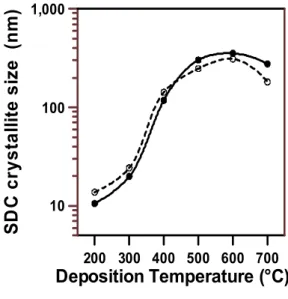
The films were deposited at deposition temperature between 200 ≤ T ≤ 700°C under a reactive oxygen atmosphere of p[O2] = 100 mTorr and varied in thickness from 500 ≤ t ≤ 1000 nm. X-ray diffraction showed that the SDC films were all single phase and could be indexed to the cubic CeO2 structure. The deposition temperature was shown to play a key role in determining the average crystallite size, preferential orientation and morphology of the as-deposited films.
The films deposited at lower temperatures (200 ≤ T ≤ 300°C) exhibited small average crystallite sizes (20 ≤ d ≤ 40 nm) but densified upon heat treatment at 500 °C forming microcracks. Films deposited at higher temperature, 400 ≤ T ≤ 700°C showed much greater average crystallite size, 100 ≤ d ≤ 300 nm and were often highly textured. SEM and AFM measurements of the film also confirmed the critical role of deposition temperature on film morphology. Electrical testing of the films
between 200 ≤ T ≤ 480°C showed that the films exhibited DC conductivities of 0.004 ≤ σ ≤ 0.01 S/cm at T = 480°C with activation energies of conduction between 0.7 ≤ Ea ≤ 0.8 eV.
References
[1] H.Yahiro, Y.Eguchi, K.Eguchi, H.Arai, J. Appl.
Electrochem,. 18, 527 (1988).
[2] H. Inaba, H.Tagawa, Solid State Ionics 83, 1 (1996). [3] C.Xia, F.Chen , M.Liu, Electrochem. Solid-State Lett.,
4, A52 (2001).
[4] T.Hibino, A.Hashimoto, T.Inoue, J.Tokuno, S.Yoshida, M.Sano, Science 288, 2031 (2000). [5] T.Hibino, A.Hashimoto, MYano, M.Suzuki, S.Yoshida, M.Sano, J. Electrochem. Soc., 149, A133 (2002).
[6] H.L.Tuller, A.S.Nowick, J. Electrochem. Soc., 122, 255 (1975).
[7] R.Doshi, V.L.Richards, J.D.Carter, X.Wang, M.Krumpelt, J. Electrochem. Soc., 146, 1273 (1999). [8] C.Milliken, S.Guruswamy, A.Khandkar, J.
Electrochem. Soc., 146, 872 (1999).
[9] J.Will, A.Mitterdorfer, C.Kleinlogel, D.Perednis, L.J.Gauckler, Solid State Ionics, 131, 79 (2000). [10] D.Perednis, L.J.Gauckler, Solid State Ionics, 166, 229 (2004).
[11] E.D.Wachsman, T.L.Clites, J. Electrochem. Soc.,
149, A242 (2002).
[12] E.D.Wachsman, Solid State Ionics, 152-153, 657 (2002).
Figures
Figure 1: Plot showing the influence of deposition temperature (Tdep) on the average crystallite size for SDC films grown by PLD. Solid line: as-deposited films; dashed line: after testing at 480 °C.
Acknowledgements:
The authors would like to thank the following people for their contributions: M. Beaulieu, J. Margeson, S. Koutcheiko and Y. Yoo for their kind technical support and I. Davidson, D. Ghosh and M. Post for helpful suggestions and support.
200 300 400 500 600 700