HAL Id: hal-01735597
https://hal.archives-ouvertes.fr/hal-01735597
Submitted on 16 Mar 2018HAL is a multi-disciplinary open access archive for the deposit and dissemination of sci-entific research documents, whether they are pub-lished or not. The documents may come from teaching and research institutions in France or abroad, or from public or private research centers.
L’archive ouverte pluridisciplinaire HAL, est destinée au dépôt et à la diffusion de documents scientifiques de niveau recherche, publiés ou non, émanant des établissements d’enseignement et de recherche français ou étrangers, des laboratoires publics ou privés.
A 12 mV start-up converter using piezoelectric
transformer for energy harvesting applications
T Martinez, Gaël Pillonnet, F. Costa
To cite this version:
T Martinez, Gaël Pillonnet, F. Costa. A 12 mV start-up converter using piezoelectric transformer for energy harvesting applications. PowerMEMS 2016, Dec 2016, Paris, France. �hal-01735597�
A 12 mV start-up converter using piezoelectric transformer for
energy harvesting applications
T Martinez1, G Pillonnet2 and F Costa1,3
1Laboratoire SATIE, ENS Paris-Saclay, France
2CEA-LETI, Université Grenoble Alpes, Grenoble, France 3Université Paris-Est, Créteil, France
E-mail: thomas.martinez@satie.ens-cachan.fr
Abstract. This paper presents a novel topology of start-up converter for sub 100 mV thermal energy
harvesting based on an Armstrong oscillator topology using a piezoelectric transformer (PT) and a normally-on MOSFET. Based on a Rosen-type PT and off-the-shelf components, the proposed start-up topology begins to oscillate at 12 mV input voltage corresponding to a temperature gradient of 2°C and achieves 1 V output voltage with only 18 mV input voltage applied to the harvester. 1. Introduction
Energy harvesting devices are a key alternative to batteries to supply low-power devices. They allow those devices to be self-autonomous without need of maintenance and with longer lifetime. In particular, thermo-electric generators (TEG) provide a DC voltage by exploiting a gradient of temperature and constitute an interesting solution to supply devices consuming less than a few mW. However, in most applications, the TEG will only provide a voltage lower than the classical threshold voltage of semi-conductors (<100 mV) that cannot then be stepped-up by classical transistor-based converters. A cold-start circuit is required to start and charge a storage device at a sufficient voltage to allow another main converter to start and realize the optimized power extraction. The start-up converter power efficiency is therefore not the most important parameter due to its short working duration in the system and the focus in the design is put on optimization of minimum start-up voltage and voltage gain.
Resonant oscillator architectures and especially the Armstrong one have been used to start at voltages as low as 40 mV [1], [2] but they suffer from bulky magnetic transformers. Piezoelectric transformers (PT’s) are a good alternative to magnetic ones as they present higher voltage gain and quality factor and limited electromagnetic radiation [3]. For exploiting PT properties in the cold-start context, the circuit proposed in [4] replaced the magnetic transformer by a piezoelectric one and used an architecture close to the half-bridge topology to obtain an inductor less converter that starts at 69 mV. Replacing a transistor with an inductance at the input allows them to decrease the start-up voltage to 32 mV.
This paper presents an alternate topology compared to [4] consisting in a self-start-up converter based on an Armstrong oscillator with a piezoelectric transformer. A biasing inductance is added at the input of the piezoelectric transformer to improve the performances. The converter has been realized experimentally
and characterized with a TEG. This converter starts with an input voltage of 12 mV and the output reaches 1 V for an input voltage of 18 mV. The paper first describes the architecture of the converter before presenting the results of the measurements.
2. Start-up converter topology based on piezoelectric transformer 2.1. Converter Topology
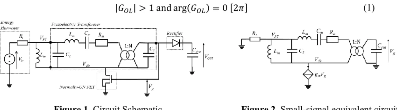
The schematic of the proposed converter is presented in Figure 1. The ideal voltage source Vin and the
resistance Rt in series respectively represent the TEG harvester’s open-circuit voltage and internal
impedance. The piezoelectric transformer consists in the two electrode capacitances C1 and C2, the RLC
series branch representing the mechanical vibration and the ideal transformer characterizing the piezoelectric effect. The converter in itself is based on the Armstrong oscillator architecture where the magnetic transformer is replaced by a piezoelectric transformer. The active component is a depletion-mode MOSFET i.e. normally-on. The circuit works as a resonant oscillator. The inherent noise in the circuit is amplified and filtered by the PT. This signal is applied to the transistor and an AC current at the selected frequency appears at the primary branch of the circuit. The PT will further amplify the amplitude of the signal and, under particular conditions, an oscillating signal appears and its amplitude increases. This signal is rectified by the diode as soon as it reaches its threshold voltage. When loss and amplification are balanced, the amplitude stops increasing and the circuit is in steady-state.
At the beginning of operation, the transistor acts as a transconductance to amplify the feedback voltage applied at its gate. However, as contrary to a magnetic transformer, the two primary side branches of the piezoelectric transformer contain a capacitive part that prevent any DC current to flow through the transistor. Subsequently the transistor has no transconductance, cannot amplify the gate voltage and no oscillation appear in the circuit. In order to solve this issue, a biasing inductance Lin is added in parallel with C1 in order
to let a DC current flow through the FET during the start-up.
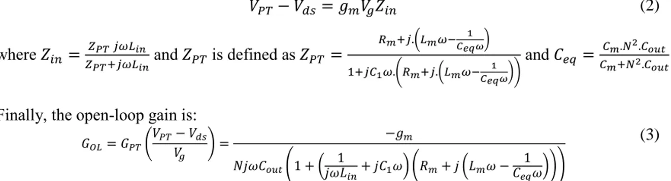
2.2. Start-up phase modelling
A small-signal analysis applied to the circuit in Figure 2 combined with the application of the Barkhausen criterion allows to find the free oscillation condition. The open-loop gain GOL of the converter can be
determined by opening the loop at the gate of the transistor. The Barkhausen criterion states that oscillation appears if the following conditions are respected:
|𝐺𝑂𝐿| > 1 and arg(𝐺𝑂𝐿) = 0 [2𝜋] (1)
Figure 1. Circuit Schematic Figure 2. Small-signal equivalent circuit The open-loop gain of the oscillator is characterized by the transconductance of the transistor, the input impedance of the piezoelectric transformer and its voltage gain. The current flowing through the FET is 𝑖𝑑𝑠= 𝑔𝑚𝑉𝑔. Thus the voltage at the input of the PT is expressed as:
where 𝑍𝑖𝑛 = 𝑍𝑃𝑇 𝑗𝜔𝐿𝑖𝑛 𝑍𝑃𝑇+𝑗𝜔𝐿𝑖𝑛 and 𝑍𝑃𝑇 is defined as 𝑍𝑃𝑇 = 𝑅𝑚+𝑗.(𝐿𝑚𝜔−𝐶𝑒𝑞𝜔1 ) 1+𝑗𝐶1𝜔.(𝑅𝑚+𝑗.(𝐿𝑚𝜔−𝐶𝑒𝑞𝜔1 )) and 𝐶𝑒𝑞= 𝐶𝑚.𝑁2.𝐶𝑜𝑢𝑡 𝐶𝑚+𝑁2.𝐶𝑜𝑢𝑡
Finally, the open-loop gain is: 𝐺𝑂𝐿= 𝐺𝑃𝑇(𝑉𝑃𝑇𝑉− 𝑉𝑑𝑠 𝑔 ) = −𝑔𝑚 𝑁𝑗𝜔𝐶𝑜𝑢𝑡(1 + (𝑗𝜔𝐿1 𝑖𝑛+ 𝑗𝐶1𝜔) (𝑅𝑚+ 𝑗 (𝐿𝑚𝜔 − 1 𝐶𝑒𝑞𝜔))) (3)
Figure 3 shows the magnitude and phase of the input impedance Zin, the voltage gain GPT and the open-loop
gain GOL. Firstly, the addition of the inductance Lin modifies the resonance frequency of the input
impedance. The oscillation frequency is defined as the one where the open-loop gain is equal to 0 according to (1). In this case, it happens close to the resonance frequency fp of Zin which is not a resonance for the PT
voltage gain GPT. As Lin increases, the oscillation frequency will be shifted away from the voltage gain
resonance frequency thus reducing the voltage gain but the input impedance value Zin will increase and so
will do the input voltage VPT –VDS. A trade-off on the Lin value appears between the PT input voltage
amplitude and the voltage gain of the PT. 3. Experimental Results
3.1. Setup description
The experimental setup is shown in Figure 4. The components were chosen to validate the model of the converter, and not in an approach of performances optimization. Their characteristics and references are summarized in table 1. The PT is a multi-layer Rosen-type PT with 55 kHz natural resonant frequency. Its output capacitance is small increasing the gain of the converter. The transistor consists in two identical depletion-mode MOSFET in parallel with a negative threshold voltage of -37 mV in order to let the current flowing at the beginning of operation. The rectifier is simply formed of a Schottky diode in series configuration. In order to test the circuit in real conditions, the measurements were realized with a TEG whose input resistance’s value is 2.8 Ω. The TEG was combined to a controlled hot plate and a heat sink to create a temperature gradient and control the voltage provided by the TEG to the circuit.
Figure 3. Magnitude and phase of the input impedance, the PT voltage gain and the total
open-loop gain.
Figure 4. PCB of the proposed start-up converter.
Table 1. Values of the circuit parameters PT SMMTF85P1S50 C1 90 nF C2 16 pF Rm 0.9 Ω Lm Cm 1.61 mH 6 nF N 45 Transistor ALD210800 Vth -37 mV β = µ0.Cox.W/L 22.4 × 10⁻³ A/V² Cg,in 4.7 pF Diode BAS70 Cdiode 2 pF Forward Voltage VF 0.41 V at IF=1 mA 3.2. Measurements
Measurements are realized with different values of the input inductance Lin. The quality factor of these
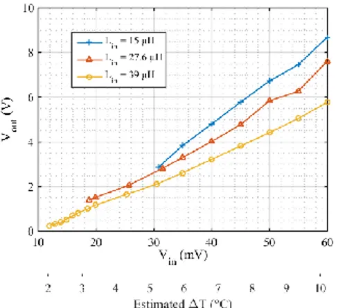
inductances is equal to 35. In Figure 5 are represented the output voltages Vout against Vin for different input
inductance values. For higher inductances, the circuit starts at smaller voltages but as soon as the circuit starts, smaller inductances achieve higher output voltages. Furthermore, the estimated temperature gradient was extracted from the open-circuit voltage and Seebeck coefficient of the TEG. For an inductance Lin =
39 µH, the circuit starts for ∆T= 2°C which corresponds to an input voltage Vin of 12 mV. Furthermore, in
this case, the output reaches 1 V for an input voltage slightly higher to 18 mV and an estimated ∆T = 3.3°C. Figure 6 represents the output voltage as a function of Lin. As expected, the higher the inductance is, the
smaller is the output voltage and an optimum value exists for Lin that will lead to a maximum output voltage.
This optimum value depends on the input voltage but in the studied range, it is between 15 and 20 µH.
Figure 5. Voltage gain for different values of the biasing inductance as a function of the input voltage and ∆T
Figure 6. Evolution of the output voltage as a function of the biasing inductance.
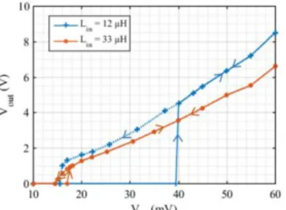
Figure 7 represents the minimum input voltage to start-up the circuit as a function of the biasing inductance Lin. An optimum value of the biasing inductance exists also for the start-up voltage as expected
we can see in Figure 8 that when the voltage increases from 0 V, the circuit starts at a specific voltage but if the voltage then decreases, the circuit will continue to operate at voltages lower than the start-up voltage leading to an hysteretic behavior. Furthermore, this figure shows the trade-off that needs to be made during the design of the circuit. If the critical aspect is the start-up voltage, high value inductances will allow to start and work at smaller voltages. On the other hand, if the minimum input voltage provided by the harvester is higher, a smaller vallue inductance will increase the voltage gain.
Figure 7. Minimum input start-up voltage of the circuit as a function of Lin
Figure 8. Hysteresis behaviour of the voltage gain
4. Conclusion
This paper presents a start-up converter with a new biasing scheme based on the Armstrong oscillator architecture with a piezoelectric transformer to achieve lower start-up input voltages. The circuit starts at voltages as low as 12 mV and can reach an output of 1 V for voltages as low as 18 mV once oscillation has started. The circuit was tested with a TEG and starts with a temperature gradient of only 2°C applied to the harvester. Compared to other start-up converters using piezoelectric transformers [4], this circuit achieves the lowest start-up voltage and highest voltage gain for similar piezoelectric transformer characteristics thanks to the proposed biasing scheme.
References
[1] J. P. Im, S. W. Wang, K. H. Lee, Y. J. Woo, Y. S. Yuk, T. H. Kong, S. W. Hong, S. T. Ryu, and G. H. Cho, “A 40mV transformer-reuse self-startup boost converter with MPPT control for thermoelectric energy harvesting,” in 2012 IEEE International Solid-State Circuits Conference, 2012, pp. 104–106. [2] S. E. Adami, V. Marian, N. Degrenne, C. Vollaire, B. Allard, and F. Costa, “Self-powered ultra-low power DC-DC converter for RF energy harvesting,” in 2012 IEEE Faible Tension Faible Consommation
(FTFC), 2012, pp. 1–4.
[3] S. S. Bedair, J. S. Pulskamp, R. G. Polcawich, B. Morgan, J. L. Martin, and B. Power, “Thin-Film Piezoelectric-on-Silicon Resonant Transformers,” J. Microelectromechanical Syst., vol. 22, no. 6, pp. 1383– 1394, Dec. 2013.
[4] A. Camarda, A. Romani, E. Macrelli, and M. Tartagni, “A 32 mV/69 mV input voltage booster based on a piezoelectric transformer for energy harvesting applications,” Sens. Actuators Phys., vol. 232, pp. 341– 352, Aug. 2015.